PDF (tesi dottorato ROTIROTI) - FedOA - Università degli Studi di ...
PDF (tesi dottorato ROTIROTI) - FedOA - Università degli Studi di ...
PDF (tesi dottorato ROTIROTI) - FedOA - Università degli Studi di ...

You also want an ePaper? Increase the reach of your titles
YUMPU automatically turns print PDFs into web optimized ePapers that Google loves.
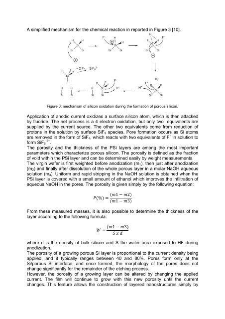
A simplified mechanism for the chemical reaction in reported in Figure 3 [10].<br />
Figure 3: mechanism of silicon oxidation during the formation of porous silicon.<br />
Application of ano<strong>di</strong>c current oxi<strong>di</strong>zes a surface silicon atom, which is then attacked<br />
by fluoride. The net process is a 4 electron oxidation, but only two equivalents are<br />
supplied by the current source. The other two equivalents come from reduction of<br />
protons in the solution by surface SiF2 species. Pore formation occurs as Si atoms<br />
are removed in the form of SiF4, which reacts with two equivalents of F − in solution to<br />
form SiF6 2− .<br />
The porosity and the thickness of the PSi layers are among the most important<br />
parameters which characterize porous silicon. The porosity is defined as the fraction<br />
of void within the PSi layer and can be determined easily by weight measurements.<br />
The virgin wafer is first weighted before ano<strong>di</strong>zation (m1), then just after ano<strong>di</strong>zation<br />
(m2) and finally after <strong>di</strong>ssolution of the whole porous layer in a molar NaOH aqueous<br />
solution (m3). Uniform and rapid stripping in the NaOH solution is obtained when the<br />
PSi layer is covered with a small amount of ethanol which improves the infiltration of<br />
aqueous NaOH in the pores. The porosity is given simply by the following equation:<br />
% <br />
<br />
1 2<br />
1 3<br />
From these measured masses, it is also possible to determine the thickness of the<br />
layer accor<strong>di</strong>ng to the following formula:<br />
1 3<br />
<br />
where d is the density of bulk silicon and S the wafer area exposed to HF during<br />
ano<strong>di</strong>zation.<br />
The porosity of a growing porous Si layer is proportional to the current density being<br />
applied, and it typically ranges between 40 and 80%. Pores form only at the<br />
Si/porous Si interface, and once formed, the morphology of the pores does not<br />
change significantly for the remainder of the etching process.<br />
However, the porosity of a growing layer can be altered by changing the applied<br />
current. The film will continue to grow with this new porosity until the current<br />
changes. This feature allows the construction of layered nanostructures simply by