PDF (tesi dottorato ROTIROTI) - FedOA - Università degli Studi di ...
PDF (tesi dottorato ROTIROTI) - FedOA - Università degli Studi di ...
PDF (tesi dottorato ROTIROTI) - FedOA - Università degli Studi di ...

Create successful ePaper yourself
Turn your PDF publications into a flip-book with our unique Google optimized e-Paper software.
Materials and Methods: Porous Silicon’ production calibration<br />
Today, the electrochemical etching is a standard method to fabricate nanostructured<br />
porous silicon: a proper choice of the applied current density, the electrolyte<br />
composition, and the silicon doping allow precise control over the morphology and,<br />
consequently, on the physical and chemical properties of the porous silicon structure.<br />
Computer controlled electrochemical etching processes are exploited for the<br />
realization of porous silicon films of controlled thickness and porosity (defined as the<br />
percentage of void in the silicon volume).<br />
Nanoporous, mesoporous and macroporous structures can be achieved, with pore<br />
size ranging from few nanometers up to microns. Moreover, since the etching<br />
process is self-stopping, it is possible to fabricate with a single run process multilayer<br />
stacks made of single layers of <strong>di</strong>fferent porosity. The <strong>di</strong>electric properties of each<br />
PSi layer, and in particular its refractive index n, can be namely modulated between<br />
those of crystalline silicon (n = 3.54, porosity = 0) and air (n= 1, porosity = 100 %); so<br />
that alternating high and low porosity layers, lot of photonic structures, such as<br />
Fabry-Perot interferometers, omni-<strong>di</strong>rectional Bragg reflectors, optical filters based on<br />
microcavities, and even complicated quasi-perio<strong>di</strong>c sequences (Thue-Morse) can be<br />
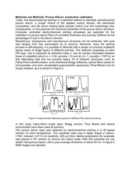
simply realized, as it is shown in Figure 5.<br />
Reflectivity (a.u)<br />
Reflectivity (a.u)<br />
1,0<br />
0,8<br />
0,6<br />
0,4<br />
0,2<br />
2,0<br />
1,5<br />
1,0<br />
0,5<br />
0,0<br />
600 800 1000 1200 1400 1600<br />
Wavelength (nm)<br />
monolayer<br />
optical microcavity<br />
800 1000 1200 1400<br />
Wavelength (nm)<br />
Reflectivity (a.u.)<br />
600 800 1000 1200 1400 1600<br />
Figure 5. Experimental reflectivity spectra of <strong>di</strong>fferent PSi optical structures.<br />
In this study Fabry-Perot single layer, Bragg mirrors, Thue Morse and optical<br />
microcavities have been used as sensors.<br />
The porous silicon layer was obtained by electrochemical etching in a HF-based<br />
solution at room temperature. The substrate used was a highly doped p + -silicon,<br />
oriented, 0.01 Ω cm resistivity, 400 μm thick. Before ano<strong>di</strong>zation the substrate<br />
was placed in HF solution to remove the native oxide. With this substrate we can<br />
obtain mesoporous layers, with a pore average <strong>di</strong>mension of about 50 nm. In figure 6<br />
SEM images are reported.<br />
1,0<br />
0,8<br />
0,6<br />
0,4<br />
0,2<br />
0,0<br />
Reflectivity (a.u)<br />
1.0<br />
0.8<br />
0.6<br />
0.4<br />
0.2<br />
0.0<br />
Bragg<br />
Wavelength (nm)<br />
Thue Morse S6<br />
600 800 1000 1200 1400 1600<br />
Wavelength (nm)