AVR 240 OM - Harman Kardon
AVR 240 OM - Harman Kardon
AVR 240 OM - Harman Kardon

You also want an ePaper? Increase the reach of your titles
YUMPU automatically turns print PDFs into web optimized ePapers that Google loves.
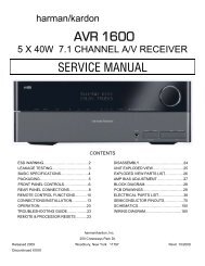
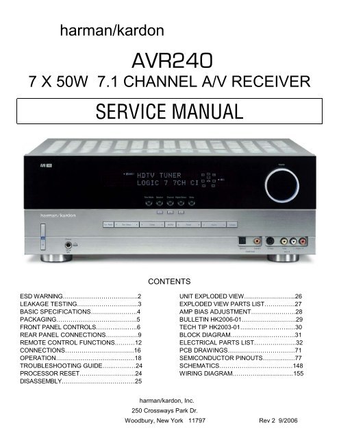
harman/kardon<br />
<strong>AVR</strong><strong>240</strong><br />
7 X 50W 7.1 CHANNEL A/V RECEIVER<br />
SERVICE MANUAL<br />
CONTENTS<br />
ESD WARNING……………………………….2<br />
LEAKAGE TESTING……………….…..…....3<br />
BASIC SPECIFICATIONS…………………..4<br />
PACKAGING………………………..………..5<br />
FRONT PANEL CONTROLS………..…..…..6<br />
REAR PANEL CONNECTIONS………….…9<br />
REMOTE CONTROL FUNCTIONS.………12<br />
CONNECTIONS………………………….…16<br />
OPERATION………………………...………18<br />
TROUBLESHOOTING GUIDE…...……..…24<br />
PROCESSOR RESET……………….….…..24<br />
DISASSEMBLY………………………………25<br />
UNIT EXPLODED VIEW……………………..26<br />
EXPLODED VIEW PARTS LIST……………27<br />
AMP BIAS ADJUSTMENT………………….28<br />
BULLETIN HK2006-01……………..……….29<br />
TECH TIP HK2003-01…...….….………..…30<br />
BLOCK DIAGRAM…………………………..31<br />
ELECTRICAL PARTS LIST………………...32<br />
PCB DRAWINGS……………………………71<br />
SEMICONDUCTOR PINOUTS……….……77<br />
SCHEMATICS………………………………148<br />
WIRING DIAGRAM………….....................155<br />
harman/kardon, Inc.<br />
250 Crossways Park Dr.<br />
Woodbury, New York 11797 Rev 2 9/2006
<strong>AVR</strong><strong>240</strong><br />
harman/kardon<br />
Some semiconductor (solid state) devices can be damaged easily by static electricity. Such components commonly are called<br />
Electrostatically Sensitive (ES) Devices. Examples of typical ES devices are integrated circuits and some field effect transistors and<br />
semiconductor "chip" components.<br />
The following techniques should be used to help reduce the incidence of component damage caused by static electricity.<br />
1. Immediately before handling any semiconductor component or semiconductor-equipped assembly, drain off any electrostatic charge on<br />
your body by touching a known earth ground. Alternatively, obtain and wear a commercially available discharging wrist strap device,<br />
which should be removed for potential shock reasons prior to applying power to the unit under test.<br />
2. After removing an electrical assembly equipped with ES devices, place the assembly on a conductive surface such as aluminum foil, to<br />
prevent electrostatic charge build-up or exposure of the assembly.<br />
3. Use only a grounded-tip soldering iron to solder or unsolder ES devices.<br />
4. Use only an anti-static solder removal device. Some solder removal devices not classified as "anti-static" can generate electrical charges<br />
sufficient to damage ES devices.<br />
5. Do not use freon-propelled chemicals. These can generate electrical change sufficient to damage ES devices.<br />
6. Do not remove a replacement ES device from its protective package until immediately before you are ready to install it. (Most replacement<br />
ES devices are packaged with leads electrically shorted together by conductive foam, aluminum foil or comparable conductive material.)<br />
7. Immediately before removing the protective material from the leads of a replacement ES device, touch the protective material to the<br />
chassis or circuit assembly into which the device will be installed.<br />
CAUTION : Be sure no power is applied to the chassis or circuit, and observe all other safety precautions.<br />
8. Minimize bodily motions when handling unpackaged replacement ES devices. (Otherwise harmless motion such as the brushing together<br />
or your clothes fabric or the lifting of your foot from a carpeted floor can generate static electricity sufficient to damage an ES devices.<br />
Each precaution in this manual should be followed during servicing.<br />
Components identified with the IEC symbol<br />
in the parts list are special significance to safety. When replacing a component identified with<br />
, use only the replacement parts designated, or parts with the same ratings or resistance, wattage, or voltage that are designated in the<br />
parts list in this manual. Leakage-current or resistance measurements must be made to determine that exposed parts are acceptably<br />
insulated from the supply circuit before retuming the product to the customer.
<strong>AVR</strong><strong>240</strong><br />
harman/kardon<br />
SAFETY PRECAUTIONS<br />
The following check should be performed for the continued<br />
protection of the customer and service technician.<br />
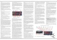
LEAKAGE CURRENT CHECK<br />
Measure leakage current to a known earth ground (water<br />
pipe, conduit, etc.) by connecting a leakage current tester<br />
between the earth ground and all exposed metal parts of the<br />
appliance (input/output terminals, screwheads, metal<br />
overlays, control shaft, etc.). Plug the AC line cord of the<br />
appliance directly into a 120V AC 60Hz outlet and turn the<br />
AC power switch on. Any current measured must not exceed<br />
o.5mA.<br />
Device<br />
under<br />
test<br />
Leakage<br />
current<br />
tester<br />
Reading should<br />
not be above<br />
0.5mA<br />
Test all<br />
exposed metal<br />
surfaces<br />
Also test with<br />
plug reversed<br />
(Using AC adapter<br />
plug as required)<br />
Earth<br />
ground<br />
AC Leakage Test<br />
ANY MEASUREMENTS NOT WITHIN THE LIMITS<br />
OUTLINED ABOVE ARE INDICATIVE OF A<br />
POTENTIAL SHOCK HAZARD AND MUST BE<br />
CORRECTED BEFORE RETURNING THE APPLIANCE<br />
TO THE CUST<strong>OM</strong>ER.<br />
3
<strong>AVR</strong><strong>240</strong><br />
harman/kardon<br />
<strong>AVR</strong> <strong>240</strong> TECHNICAL SPECIFICATIONS<br />
Audio Section<br />
Stereo Mode<br />
Continuous Average Power (FTC)<br />
65 Watts per channel, 20Hz–20kHz,<br />
@
<strong>AVR</strong><strong>240</strong><br />
harman/kardon<br />
FRONT-PANEL CONTROLS<br />
˜<br />
ˆ<br />
ı<br />
Ù<br />
Û<br />
Ú<br />
Ò<br />
apple<br />
<strong>AVR</strong> <strong>240</strong><br />
DIGITAL LOGIC 7 VID 1 DVD<br />
PRO LOGIC<br />
3 STEREO DSP<br />
5 7 CH. STEREO<br />
SURR. OFF<br />
VID 2<br />
VID 3<br />
VID 4<br />
CD<br />
FMAM<br />
TAPE<br />
6 8 CH<br />
Optical 3 Coaxial 3<br />
Video 4<br />
1 3<br />
5 7 9 ! # %<br />
2 4 6<br />
8 ) @ ) $ ^<br />
&<br />
(<br />
Ô<br />
*<br />
Ó<br />
NOTE: To make it easier to follow the instructions that refer to this illustration, a larger copy may be downloaded from the Product Support section for this product<br />
at www.harmankardon.com.<br />
1 Main Power Switch<br />
2 Power Indicator<br />
3 Standby/On Switch<br />
4 Headphone Jack<br />
5 Tone Mode<br />
6 Speaker Selector<br />
7 Surround Mode Group Selector<br />
8 Surround Mode Selector<br />
9 Tuning Selector<br />
) ‹/› Buttons<br />
! Tuner Band Selector<br />
@ Set Button<br />
# Digital Input Selector<br />
$ Preset Station Selector<br />
% Delay Adjust Selector<br />
^ Input Source Selector<br />
& Tuner Mode Selector<br />
* Optical 3 Digital Audio Input<br />
( Coaxial 3 Digital Audio Input<br />
Ó Video 4 Video Input Jacks<br />
Ô Video 4 Audio Input Jacks<br />
apple Channel Adjust Selector<br />
Ò Volume Control<br />
Ú Input Indicators<br />
Û Speaker/Channel Input Indicators<br />
Ù Upper Display Line<br />
ı Lower Display Line<br />
ˆ Surround Mode Indicators<br />
˜ Remote Sensor Window<br />
1 Main Power Switch: Press this button to apply<br />
power to the <strong>AVR</strong> <strong>240</strong>. When the switch is pressed<br />
in, the unit is in a Standby mode, as indicated by the<br />
amber Power Indicator 2. This button MUST be<br />
pressed in to operate the unit. To turn the unit off and<br />
prevent the use of the remote control, this switch<br />
should be pressed until it pops out from the front<br />
panel and the word “OFF” is seen at the top of the<br />
switch.<br />
NOTE: This switch is normally left in the “ON” position.<br />
2 Power Indicator: This LED lights amber when the<br />
unit is in the Standby mode to signal that the <strong>AVR</strong> is<br />
ready to be turned on. When the unit is in operation,<br />
the indicator is blue.<br />
3 Standby/On Switch: When the Main Power<br />
Switch 1 is “ON,” press this button to turn on the<br />
<strong>AVR</strong> <strong>240</strong>; press it again to turn the unit off. The Power<br />
Indicator 2 turns blue when the unit is on.<br />
4 Headphone Jack: This jack may be used to listen<br />
to the <strong>AVR</strong> <strong>240</strong>’s output through a pair of headphones.<br />
The speakers will automatically be turned off when the<br />
headphone jack is in use. When configuring your system<br />
using EzSet+, the calibration microphone should<br />
be plugged into this jack using the supplied adaptor<br />
that converts the small mini-plug at the end of the<br />
microphone’s cord to a 1/4" plug.<br />
5 Tone Mode: This button controls the tone mode<br />
settings, enabling adjustment of the bass and treble<br />
boost/cut. You may also use it to take the tone controls<br />
out of the signal path completely for “flat”<br />
response. The first press of the button displays a<br />
TONE IN message in the Lower Display Line<br />
ı and in the on-screen display. To take the controls<br />
out of the signal path, press either of the ‹/›<br />
Buttons ) until the display reads TONE OUT.<br />
To change the bass or treble settings, make sure that<br />
TONE IN appears in the Lower Display Line ı<br />
or press either of the ‹/› Buttons ) until it does.<br />
Press the Tone Mode Button 5 until the desired<br />
option of TREBLE MODE or BASS MODE<br />
appears in the Lower Display Line ı and in the<br />
on-screen display and then press either of the ‹/›<br />
Buttons ) to enter the desired boost or cut setting.<br />
Both treble and bass contours may be boosted or<br />
cut by up to + or –10dB in increments of 2dB. See<br />
pages 21 and 31 for more information on the tone<br />
controls.<br />
NOTE: The <strong>AVR</strong> <strong>240</strong> is not equipped with a traditional<br />
Balance control. When listening to two-channel materials,<br />
if you wish to adjust the stereo image, you may<br />
use the Channel Adjust Selector apple to increase or<br />
decrease the level of the left front channel by up to +<br />
or –10dB, and then to decrease or increase the right<br />
front channel by the corresponding amount. However,<br />
when listening to surround materials and most twochannel<br />
materials, it is recommended that you leave<br />
these settings at the results obtained during the configuration<br />
process described on pages 19 through 30.<br />
6<br />
FRONT-PANEL CONTROLS 5
<strong>AVR</strong><strong>240</strong><br />
FRONT-PANEL CONTROLS<br />
harman/kardon<br />
6 Speaker Selector: Press this button to begin<br />
the process of configuring the unit to match the type<br />
of speakers used in your listening room. (See pages<br />
26–28 for more information on speaker setup and<br />
configuration.)<br />
7 Surround Mode Group Selector: Press this button<br />
to select the top-level group of surround modes.<br />
Each press of the button will select the current or last<br />
used mode in each of the surround mode groups<br />
(e.g., Dolby, DTS, DTS Neo:6, Logic 7, DSP, Stereo).<br />
When the button is pressed so that the name of the<br />
surround mode group appears in the on-screen display<br />
and in the Lower Display Line ı, press the<br />
Surround Mode Selector 8 to cycle through the<br />
individual modes available. For example, press this<br />
button to select Dolby modes, and then press the<br />
Surround Mode Selector 8 to choose from the<br />
various Dolby mode options.<br />
8 Surround Mode Selector: Press this button<br />
to select from among the available surround mode<br />
options for the mode group selected. The specific<br />
modes will vary based on the number of speakers<br />
available, the mode group and if the input source is<br />
digital or analog. For example, press the Surround<br />
Mode Group Selector 7 to select a main mode<br />
grouping such as Dolby or Logic 7, and then press<br />
this button to see the specific mode choices available.<br />
Note that the digital surround modes, such as Dolby<br />
Digital and DTS, may not be accessed unless that type<br />
of source signal is present, such as when a DVD movie<br />
or television signal programmed in Dolby Digital or DTS<br />
surround sound is playing. For more information on surround<br />
mode selection, see pages 23 and 32.<br />
9 Tuning Selector: Press the left side of the button<br />
to tune lower-frequency stations and the right side of<br />
the button to tune higher-frequency stations. When the<br />
tuner is in the Manual mode, each tap will increase or<br />
decrease the frequency by one increment. When the<br />
tuner receives a strong enough signal for adequate<br />
reception, MANUAL TUNED will appear in the<br />
on-screen display and the Lower Display Line ı.<br />
When the tuner is the Auto mode, press the button<br />
once, and the tuner will scan for a station with acceptable<br />
signal strength. When the next station with a<br />
strong signal is tuned the scan will stop and the<br />
on-screen display and Lower Display Line ı<br />
will indicate AUTO TUNED. When an FM<br />
Stereo station is tuned, the display will read<br />
AUTO ST TUNED.<br />
To switch back and forth between the Auto and<br />
Manual tuning modes, press the Tuner Mode<br />
Selector &.<br />
) ‹/› Buttons: When configuring the <strong>AVR</strong> <strong>240</strong>’s<br />
settings, use these buttons to select from the available<br />
choices.<br />
! Tuner Band Selector: Press this button to turn<br />
the <strong>AVR</strong> on and to select the Tuner as the input. Press<br />
it again to switch between the AM and FM frequency<br />
bands. (See page 37 for more information on the tuner.)<br />
@ Set Button: When making choices during the<br />
setup and configuration process, press this button<br />
to enter the desired setting into the <strong>AVR</strong> <strong>240</strong>’s memory.<br />
# Digital Input Selector: Press this button to<br />
select one of the digital audio inputs or the analog<br />
audio input for any source. (See pages 32–37 for<br />
more information on digital audio.)<br />
$ Preset Stations Selector: Press this button to<br />
scroll up or down through the list of stations that have<br />
been entered into the preset memory. (See page 37<br />
for more information on tuner presets.)<br />
% Delay Adjust Selector: Press this button to<br />
begin the steps required to enter delay settings. (See<br />
pages 28–29 for more information on delay times.)<br />
^ Input Source Selector: Press this button to<br />
change the input by scrolling up or down through the<br />
list of Input Indicators Ú.<br />
& Tuner Mode Selector: Press this button to select<br />
Auto or Manual tuning. When the button is pressed so<br />
that the AUTO appears in the Lower Display Line<br />
ı, the tuner will search for the next station with an<br />
acceptable signal when the Tuning Selector 9u<br />
is pressed. When the button is pressed so that<br />
MANUAL appears in the Lower Display Line ı,<br />
each press of the Tuning Selector 9u will<br />
increase the frequency. This button may also be used to<br />
switch between Stereo and Mono modes for FM radio<br />
reception. When weak reception is encountered, press<br />
the button so that MANUAL appears in the Lower<br />
Display Line ı and on the on-screen display to<br />
switch to Mono reception. Press it again to switch back<br />
to Stereo mode. (See page 37 for more information on<br />
using the tuner.)<br />
* Optical 3 Digital Audio Input: Connect the optical<br />
digital audio output of an audio or video product to this<br />
jack. When the input is not in use, the built-in shutter will<br />
close to avoid dust contamination that might degrade<br />
future performance.<br />
( Coaxial 3 Digital Audio Input: This jack is used<br />
for connection to the output of portable audio devices,<br />
video game consoles or other products that have a<br />
coax digital audio jack.<br />
Ó Video 4 Video Input Jacks: These jacks may<br />
be used for temporary connection to the composite or<br />
S-video output of video games, camcorders or other<br />
portable video products. You may make a connection<br />
to either jack at any time, but not to both simultaneously.<br />
Ô Video 4 Audio Input Jacks: These audio jacks<br />
may be used for temporary connection to video<br />
games or portable audio/video products such as<br />
camcorders and portable audio players.<br />
apple Channel Adjust Selector: Press this button to<br />
begin the process of trimming the channel output levels<br />
using an external audio source. (For more information<br />
on output level trim adjustment, see page 38.)<br />
Ò Volume Control: Turn this knob clockwise to<br />
increase the volume, counterclockwise to decrease<br />
the volume. If the <strong>AVR</strong> <strong>240</strong> is muted, adjusting the<br />
Volume Control Ò will automatically release<br />
the unit from the silenced condition.<br />
Ú Input Indicators: The current selected source<br />
will appear as one of these indicators. When the unit<br />
is turned on, the entire list of available modes will<br />
light briefly, and then revert to normal operation with<br />
only the active mode indicator illuminated.<br />
The<br />
BridgeTM<br />
NOTE: When /DMP has been selected as<br />
the input source, no Input Indicator N will light.<br />
DMP/THE BRIDGE IS CONNECTED<br />
will scroll across the Upper Display Line P, unless<br />
you have retitled the source name, in which case that<br />
name will appear. See page 20 for more information<br />
on input titling.<br />
Û Speaker/Channel Input Indicators: These indicators<br />
are multipurpose, indicating both the speaker<br />
type selected for each channel and the incoming datasignal<br />
configuration. The left, center, right, right surround<br />
and left surround speaker indicators are composed of<br />
three boxes, while the subwoofer is a single box. The<br />
center box lights when a “small” speaker is selected,<br />
and the two outer boxes light when “large” speakers are<br />
selected. When none of the boxes are lit for the center,<br />
surround or subwoofer channels, no speaker has been<br />
assigned that position. (See pages 26–28 for more<br />
information on configuring speakers.)<br />
The letters inside each box display the active input<br />
channels. For standard analog sources, only the L and R<br />
will light, indicating a stereo input. For a digital source,<br />
the indicators will light to display the channels being<br />
received at the digital input. When the letters flash, the<br />
digital input has been interrupted. (See page 36 for<br />
more information on the Channel Indicators.)<br />
Ù Upper Display Line: Depending on the unit’s status,<br />
a variety of messages will appear here. In normal<br />
6 FRONT-PANEL CONTROLS<br />
7
<strong>AVR</strong><strong>240</strong><br />
harman/kardon<br />
FRONT-PANEL CONTROLS<br />
operation, this line will show current input source and<br />
which analog or digital input is in use. When the tuner is<br />
the input, this line will identify the station as AM or FM<br />
and show the frequency and preset number, if any.<br />
ı Lower Display Line: Depending on the unit’s status,<br />
a variety of messages will appear here. In normal<br />
operation, the current surround mode will show here.<br />
ˆ Surround Mode Indicators: The current selected<br />
surround mode will appear as one of these indicators.<br />
Note that when the unit is turned on, the entire list of<br />
available modes will light briefly, and then revert to<br />
normal operation with only the active mode indicator<br />
illuminated.<br />
NOTE: When the Dolby Virtual Speaker or Dolby<br />
Headphone modes are in use, no Surround Mode<br />
Indicator R will light. However, the surround mode<br />
name will scroll in the Lower Display Line Q.<br />
˜ Remote Sensor Window: The sensor behind<br />
this window receives infrared signals from the remote<br />
control. Aim the remote at this area and do not block<br />
or cover it.<br />
8<br />
FRONT-PANEL CONTROLS 7
The Bridge<br />
<strong>AVR</strong><strong>240</strong><br />
REAR-PANEL CONNECTIONS<br />
harman/kardon<br />
<br />
<br />
<br />
<br />
<br />
j<br />
h<br />
f<br />
d<br />
b<br />
·<br />
‡<br />
<br />
<br />
<br />
<br />
k<br />
i<br />
g<br />
e<br />
c<br />
a<br />
°<br />
fl<br />
¡<br />
<br />
£<br />
¢<br />
∞<br />
§<br />
•<br />
ª ‚ ⁄ ¤ ‹ › fi<br />
NOTE: To make it easier to follow the instructions that refer to this illustration, a larger copy may be downloaded from the Product Support section for this product<br />
at www.harmankardon.com.<br />
¡ FM Antenna Jack<br />
CD Audio Inputs<br />
£ Tape Outputs<br />
¢ Tape Inputs<br />
∞ Remote IR Input<br />
§ Remote IR Output<br />
Preamp Outputs<br />
• Subwoofer Output<br />
ª Front Speaker Outputs<br />
‚ Surround Back Speaker Outputs<br />
⁄ Surround Speaker Outputs<br />
¤ Center Speaker Outputs<br />
‹ Component Video Monitor Outputs<br />
› Component Video 1 Inputs<br />
fi Component Video 2 Inputs<br />
fl AC Power Cord<br />
‡ Switched AC Accessory Outlet<br />
° Unswitched AC Accessory Outlet<br />
· Optical Digital Audio Output<br />
a Coaxial Digital Audio Output<br />
b Coaxial Digital Audio Inputs<br />
c S-Video Monitor Output<br />
d DVD S-Video Input<br />
The<br />
BridgeTM<br />
e DMP Connector<br />
f Video 1 S-Video Input<br />
g Optical Digital Audio Inputs<br />
h Video 1 S-Video Output<br />
i Video 2 S-Video Input<br />
j 6/8-Channel Direct Inputs<br />
k Video 2 S-Video Output<br />
Video 3 S-Video Input<br />
Video Monitor Output<br />
DVD Audio/Video Inputs<br />
Video 1 Audio/Video Inputs<br />
Video 1 Audio/Video Outputs<br />
Video 2 Audio/Video Inputs<br />
Video 2 Audio/Video Outputs<br />
Video 3 Audio/Video Inputs<br />
AM Antenna Terminals<br />
NOTE: To assist in making the correct connections<br />
for multichannel input, output and speaker connections,<br />
all connection jacks and terminals are colorcoded<br />
in conformance with the CEA standards as<br />
follows:<br />
Front Left:<br />
White<br />
Front Right: Red<br />
Center:<br />
Surround Left:<br />
Surround Right:<br />
Surround Back Left:<br />
Surround Back Right:<br />
Subwoofer:<br />
Coaxial Digital Audio:<br />
Green<br />
Blue<br />
Gray<br />
Brown<br />
Tan<br />
Purple<br />
Orange<br />
Composite Video: Yellow<br />
Component Video “Y”: Green<br />
Component Video “Pr”: Red<br />
Component Video “Pb”: Blue<br />
¡ FM Antenna Jack: Connect the supplied indoor<br />
(or an optional external) FM antenna to this terminal.<br />
CD Audio Inputs: Connect these jacks to the<br />
analog audio outputs of a compact disc player or<br />
CD changer.<br />
£ Tape Outputs: Connect these jacks to the<br />
RECORD/INPUT jacks of an audio recorder.<br />
¢ Tape Inputs: Connect these jacks to the<br />
PLAY/OUT jacks of an audio recorder.<br />
∞ Remote IR Input: If the <strong>AVR</strong> <strong>240</strong>’s front-panel<br />
IR sensor is blocked due to cabinet doors or other<br />
obstructions, an external IR sensor may be used.<br />
Connect the output of the sensor to this jack.<br />
8 REAR-PANEL CONNECTIONS<br />
9
<strong>AVR</strong><strong>240</strong><br />
harman/kardon<br />
REAR-PANEL CONNECTIONS<br />
§ Remote IR Output: This connection permits the<br />
IR sensor in the receiver to serve other remote controlled<br />
devices. Connect this jack to the “IR IN” jack on<br />
<strong>Harman</strong> <strong>Kardon</strong> (or other compatible) equipment.<br />
Preamp Outputs: Connect these jacks to an<br />
optional, external power amplifier for applications<br />
where higher power is desired.<br />
• Subwoofer Output: Connect this jack to the linelevel<br />
input of a powered subwoofer. If an external subwoofer<br />
amplifier is used, connect this jack to the subwoofer<br />
amplifier input.<br />
ª Front Speaker Outputs: Connect these outputs<br />
to the matching + or – terminals on your left and right<br />
speakers. When making speaker connections always<br />
make certain to maintain correct polarity by connecting<br />
the color-coded (white for front left and red for front<br />
right) (+) terminals on the <strong>AVR</strong> <strong>240</strong> to the red (+)<br />
terminals on the speakers and the black (–) terminals<br />
on the <strong>AVR</strong> <strong>240</strong> to the black (–) terminals on the<br />
speakers. See page 15 for more information on<br />
speaker polarity.<br />
‚ Surround Back Speaker Outputs: These<br />
speaker terminals are normally used to power the<br />
surround back speakers in a 7.1-channel system.<br />
Connect these outputs to the matching + and –<br />
terminals on your surround back channel speaker.<br />
In conformance with the CEA color-code specification,<br />
the brown terminal is the positive, or “+,” terminal that<br />
should be connected to the red (+) terminal on the<br />
left Surround Back speaker with older color-coding.<br />
The tan terminal is the positive, or “+”, terminal that<br />
should be connected to the red (+) terminal on the<br />
right Surround Back speaker with older color-coding.<br />
Connect the black (–) terminals on the <strong>AVR</strong> to the<br />
matching black negative (–) terminals on the surround<br />
back speakers. (See page 15 for more information on<br />
speaker polarity.)<br />
⁄ Surround Speaker Outputs: Connect these outputs<br />
to the matching + and – terminals on your surround<br />
channel speakers. In conformance with the CEA<br />
color-code specification, the blue terminal is the positive,<br />
or “+,” terminal that should be connected to the<br />
red (+) terminal on the Surround Left speaker with<br />
older color-coding, while the gray terminal should be<br />
connected to the red (+) terminal on the Surround<br />
Right speaker with the older color-coding. Connect the<br />
black (–) terminal on the <strong>AVR</strong> to the matching black<br />
negative (–) terminals for each surround speaker. (See<br />
page 15 for more information on speaker polarity.)<br />
¤ Center Speaker Outputs: Connect these outputs<br />
to the matching + and – terminals on your center<br />
channel speaker. In conformance with the CEA<br />
color-code specification, the green terminal is the<br />
positive, or “+,” terminal that should be connected to<br />
the red (+) terminal on speakers with the older colorcoding.<br />
Connect the black (–) terminal on the <strong>AVR</strong> to<br />
the black (–) terminal on your speaker. (See page 15<br />
for more information on speaker polarity.)<br />
‹ Component Video Monitor Outputs: Connect<br />
these outputs to the component video inputs of a<br />
video projector or monitor. When a source connected<br />
to one of the Component Video Inputs ›fi is<br />
selected, the signal will be sent to these jacks.<br />
› Component Video 1 Inputs: Connect the<br />
Y/Pr/Pb component video outputs of a DVD player,<br />
HDTV set-top converter, satellite receiver or other<br />
video source device with component video outputs to<br />
these jacks.<br />
fi Component Video 2 Inputs: Connect the<br />
Y/Pr/Pb component video outputs of a DVD player,<br />
HDTV set-top converter, satellite receiver or other<br />
video source device with component video outputs to<br />
these jacks.<br />
See page 20 for information on assigning the<br />
Component Video 1 and 2 Inputs ›fi to the<br />
appropriate source inputs.<br />
fl AC Power Cord: Connect the AC power cord to<br />
a non-switched AC wall outlet.<br />
‡ Switched AC Accessory Outlet: These outlets<br />
may be used to power any device you wish to have<br />
turned on when the <strong>AVR</strong> <strong>240</strong> is turned on.<br />
° Unswitched AC Accessory Outlet: This outlet<br />
may be used to power any AC device. The power will<br />
remain on at this outlet regardless of whether the<br />
<strong>AVR</strong> <strong>240</strong> is on or off.<br />
NOTE: The total power consumption of all devices<br />
connected to the accessory outlets should not exceed<br />
100 watts.<br />
· Optical Digital Audio Output: Connect this jack<br />
to the optical digital input connector on a CD-R/RW,<br />
MiniDisc or other digital recorder.<br />
a Coaxial Digital Audio Output: Connect this jack<br />
to the coaxial digital input of a CD-R/RW, MiniDisc or<br />
other digital recorder.<br />
b Coaxial Digital Audio Inputs: Connect the coax<br />
digital output from a DVD player, HDTV receiver, LD<br />
player or CD player to these jacks. The signal may be a<br />
Dolby Digital signal, DTS signal or a standard PCM digital<br />
source. Do not connect the RF digital output of an LD<br />
player to these jacks.<br />
c S-Video Monitor Output: If any of the input<br />
sources used in your system have S-video connections<br />
to the <strong>AVR</strong>, connect this jack to the S-video input<br />
on your television, projector or other video display.<br />
d DVD S-Video Input: Connect the S-video output of<br />
a DVD player or other video source to this jack.<br />
The<br />
BridgeTM<br />
e Digital Media Player (DMP) Connector:<br />
With the <strong>AVR</strong> <strong>240</strong> turned off, connect the optional<br />
The<br />
BridgeTM<br />
<strong>Harman</strong> <strong>Kardon</strong> to this connector. When the<br />
Digital Media Player source is selected, you may view<br />
iPod control and navigation messages on your video<br />
display (if one is connected to one of the Video<br />
Monitor Outputs c), and in the Upper and Lower<br />
Display Lines PQ. You may navigate the iPod<br />
and select tracks for playback using the ⁄/¤/‹/›<br />
Buttons no, the Set Button p and Transport<br />
Controls ` on your <strong>AVR</strong> remote. See page 37 for<br />
more information.<br />
f Video 1 S-Video Input: If the product connected to<br />
the Video 1 Audio Inputs has S-video capability,<br />
connect this jack to the PLAY/OUT S-video jack on<br />
that unit and then make certain that the S-Video<br />
Monitor Output c is connected as described above.<br />
g Optical Digital Audio Inputs: Connect the optical<br />
digital output from a DVD player, HDTV receiver,LD<br />
player or CD player to these jacks. The signal may be a<br />
Dolby Digital signal, a DTS signal or a standard PCM<br />
digital source.<br />
h Video 1 S-Video Output: If the product connected<br />
to the Video 1 Audio/Video Outputs has S-video<br />
capability, connect this jack to the REC/IN S-video jack<br />
on that unit.<br />
i Video 2 S-Video Input: If the product connected<br />
to the Video 2 Audio/Video Inputs has S-video<br />
capability, connect this jack to the PLAY/OUT S-video<br />
jack on that unit and then make certain that the<br />
S-Video Monitor Output c is connected as<br />
described above.<br />
j 6/8-Channel Direct Inputs: These jacks are<br />
used for connection to source devices such as DVD-<br />
Audio or SACD players with discrete analog outputs.<br />
Depending on the source device in use, all eight jacks<br />
may be used, though in many cases only connections<br />
to the front left/right, center, surround left/right and<br />
LFE (subwoofer input) jacks will be used for standard<br />
5.1 audio signals.<br />
k Video 2 S-Video Output: If the product connected<br />
to the Video 2 Audio Outputs has S-video capability,<br />
connect this jack to the REC/IN S-video jack on<br />
that unit.<br />
Video 3 S-Video Input: If the product connected to<br />
the Video 3 Audio Inputs has S-video capability,<br />
connect this jack to the PLAY/OUT S-video jack on<br />
that unit and then make certain that the S-Video<br />
Monitor Output c is connected as described above.<br />
10<br />
REAR-PANEL CONNECTIONS 9
<strong>AVR</strong><strong>240</strong><br />
harman/kardon<br />
REAR-PANEL CONNECTIONS<br />
Video Monitor Output: Connect this jack to the<br />
composite video input of a TV monitor or video projector<br />
to view the on-screen menus and the output of a<br />
standard video source.<br />
DVD Audio/Video Inputs: Connect the composite<br />
video and L/R analog audio outputs of a DVD player or<br />
other video source to these jacks.<br />
Video 1 Audio/Video Inputs: Connect the composite<br />
video and L/R analog audio PLAY/OUT jacks of<br />
a VCR or other video source to these jacks.<br />
Video 1 Audio/Video Outputs: Connect the<br />
composite video and L/R analog audio REC/IN jacks<br />
of a VCR or other video recording device such as a<br />
DVD recorder or PVR to these jacks.<br />
Video 2 Audio/Video Inputs: Connect the composite<br />
video and L/R analog audio PLAY/OUT jacks<br />
of a cable television box or other video source to<br />
these jacks.<br />
Video 2 Audio/Video Outputs: Connect the<br />
composite video and L/R analog audio REC/IN jacks<br />
of a VCR or other video recording device such as a<br />
DVD recorder or PVR to these jacks.<br />
Video 3 Audio/Video Inputs: Connect the composite<br />
video and L/R analog audio PLAY/OUT jacks of<br />
an HDTV tuner or other video source to these jacks.<br />
AM Antenna Terminals: Connect the AM loop<br />
antenna supplied with the receiver to these terminals.<br />
If an external AM antenna is used, make connections<br />
to the AM and GND terminals in accordance with<br />
the instructions supplied with the antenna.<br />
NOTE ON VIDEO CONNECTIONS: When connecting<br />
a video source product such as a VCR, DVD player,<br />
satellite receiver, cable set-top box, personal video<br />
recorder or video game to the <strong>AVR</strong> <strong>240</strong>, you may<br />
use either a composite or S-video connection, but<br />
not both.<br />
10 REAR-PANEL CONNECTIONS<br />
11
<strong>AVR</strong><strong>240</strong><br />
harman/kardon<br />
REMOTE CONTROL FUNCTIONS<br />
a Power Off Button<br />
b IR Transmitter Window<br />
c Program Indicator<br />
d Power On Button<br />
e Input Selectors<br />
f <strong>AVR</strong> Selector<br />
g AM/FM Tuner Select<br />
h Dim Button<br />
i Test Button<br />
j Sleep Button<br />
k DSP Surround Mode Selector<br />
l Night Mode<br />
m Channel Select Button<br />
n ⁄/¤ Buttons<br />
o ‹ /› Buttons<br />
p Set Button<br />
q Digital Select<br />
r Numeric Keys<br />
s Tuner Mode<br />
t Direct Button<br />
u Tuning Up/Down<br />
v OSD Button<br />
w Dolby Mode Selector<br />
x DTS Digital Mode Selector<br />
y Logic 7 Mode Select Button<br />
z Skip Up/Down Buttons<br />
` Transport Controls<br />
Stereo Mode Select Button<br />
DTS Neo:6 Mode Select<br />
Macro Buttons<br />
Disc Skip Button<br />
Preset Up/Down<br />
Clear Button<br />
Memory Button<br />
Delay/Prev. Ch.<br />
Speaker Select<br />
Spare Button<br />
Volume Up/Down<br />
TV/Video Selector<br />
The<br />
BridgeTM<br />
DMP Selector<br />
6-Channel/8-Channel Direct Input<br />
Mute<br />
e<br />
g<br />
i<br />
k<br />
m<br />
o<br />
q<br />
s<br />
u<br />
w<br />
y<br />
d<br />
f<br />
h<br />
j<br />
l<br />
n<br />
p<br />
n<br />
r<br />
t<br />
v<br />
x<br />
z<br />
GUIDE<br />
EXIT<br />
c ba<br />
POWER<br />
ON<br />
OFF MUTE<br />
<strong>AVR</strong> DVD CD TAPE<br />
VCR CBL/SAT TV<br />
VID 1 VID 2 VID3 VID4<br />
The<br />
BridgeTM<br />
DIM AM/FM 6/8 CH DMP<br />
SLEEP<br />
TEST T/V<br />
CH. NIGHT<br />
VOL.<br />
SURR.<br />
CH.<br />
DIGITAL<br />
SET<br />
SPKR<br />
MENU<br />
DELAY<br />
1 2 3 4<br />
5 6 7 8<br />
9 0<br />
TUN-M MEM<br />
PREV.CH.<br />
DIRECT CLEAR<br />
TUNING<br />
PRESET<br />
OSD D.SKIP<br />
M1 M2 M3 M4<br />
DOLBY SUR DTS SUR DTS NEO:6<br />
LOGIC 7 STEREO<br />
DOWN<br />
SKIP UP<br />
42<br />
40<br />
38<br />
36<br />
o<br />
34<br />
32<br />
30<br />
28<br />
41<br />
39<br />
37<br />
35<br />
33<br />
31<br />
29<br />
NOTES:<br />
• The function names shown here are each button’s<br />
feature when used with the <strong>AVR</strong> <strong>240</strong>. Most buttons<br />
have additional functions when used with other<br />
devices. See pages 44–45 for a list of these<br />
functions.<br />
• To make it easier to follow the instructions that refer<br />
to this illustration, a larger copy may be downloaded<br />
from the Product Support section for this<br />
product at www.harmankardon.com.<br />
<strong>240</strong><br />
®<br />
`<br />
12<br />
REMOTE CONTROL FUNCTIONS 11
<strong>AVR</strong><strong>240</strong><br />
REMOTE CONTROL FUNCTIONS<br />
harman/kardon<br />
IMPORTANT NOTE: The <strong>AVR</strong> <strong>240</strong>’s remote may<br />
be programmed to control up to seven devices,<br />
including the <strong>AVR</strong> <strong>240</strong>. Before using the remote, it is<br />
important to remember to press the Input Selector<br />
Button e that corresponds to the unit you wish to<br />
operate. In addition, the <strong>AVR</strong> <strong>240</strong>’s remote is shipped<br />
from the factory to operate the <strong>AVR</strong> <strong>240</strong> and most<br />
<strong>Harman</strong> <strong>Kardon</strong> CD or DVD players and cassette<br />
decks. The remote is also capable of operating a wide<br />
variety of other products using the control codes that<br />
are part of the remote. Before using the remote with<br />
other products, follow the instructions on page 41<br />
to program the proper codes for the products in<br />
your system.<br />
It is also important to remember that many of the buttons<br />
on the remote take on different functions, depending<br />
on the product selected using the Device Control<br />
Selectors. The descriptions shown here primarily detail<br />
the functions of the remote when it is used to operate<br />
the <strong>AVR</strong> <strong>240</strong>. (See pages 42–45 for information about<br />
alternate functions for the remote’s buttons.)<br />
a Power Off Button: Press this button to place the<br />
<strong>AVR</strong> <strong>240</strong> or a selected device in the Standby mode.<br />
b IR Transmitter Window: Point this window<br />
towards the <strong>AVR</strong> <strong>240</strong> when pressing buttons on the<br />
remote to make certain that infrared commands are<br />
properly received.<br />
c Program Indicator: This three-color indicator is<br />
used to guide you through the process of programming<br />
the remote. (See page 41 for information on<br />
programming the remote.)<br />
d Power On Button: Press this button to turn on<br />
the power to a device selected by pressing one of the<br />
Input Selectors e.<br />
e Input Selectors: Pressing one of these buttons<br />
will perform three actions at the same time. First, if the<br />
<strong>AVR</strong> <strong>240</strong> is not turned on, this will power up the unit.<br />
Next, it will select the source shown on the button as<br />
the input to the <strong>AVR</strong> <strong>240</strong>. Finally, it will change the<br />
remote control so that it controls the device selected.<br />
After pressing one of these buttons you must press<br />
the <strong>AVR</strong> Selector Button f again to operate the<br />
<strong>AVR</strong> <strong>240</strong>’s functions with the remote.<br />
f <strong>AVR</strong> Selector: Pressing this button will switch the<br />
remote so that it will operate the <strong>AVR</strong> <strong>240</strong>’s functions. If<br />
the <strong>AVR</strong> <strong>240</strong> is in the Standby mode, it will also turn the<br />
<strong>AVR</strong> <strong>240</strong> on.<br />
g AM/FM Tuner Select: Press this button to select<br />
the <strong>AVR</strong> <strong>240</strong>’s tuner as the listening choice. Pressing<br />
this button when the tuner is already in use will select<br />
between the AM and FM bands.<br />
h Dim Button: Press this button to activate the<br />
Dimmer function, which reduces the brightness of the<br />
front panel display, or turns it off entirely. The first press<br />
of the button shows the default state, which is full brightness<br />
by indicating VFD FULL in the Lower<br />
Display Line ı. Press the button again within five<br />
seconds to reduce the brightness by 50%, as indicated<br />
by VFD HALF showing in the Lower Display Line<br />
ı. Press the button again within five seconds and the<br />
main display will go completely dark. Note that this setting<br />
is temporary, in that regardless of any changes, the<br />
display will always return to full brightness when the <strong>AVR</strong><br />
is turned on. In addition, the Power Indicator 2 will<br />
always remain at full brightness regardless of the setting.<br />
This is to remind you that the <strong>AVR</strong> is still turned on.<br />
i Test Button: Press this button to begin the<br />
sequence used to calibrate the <strong>AVR</strong> <strong>240</strong>’s output levels.<br />
(See pages 25, 29 and 38 for more information on<br />
calibrating the <strong>AVR</strong> <strong>240</strong>.)<br />
j Sleep Button: Press this button to place the unit<br />
in the Sleep mode. After the time shown in the display,<br />
the <strong>AVR</strong> <strong>240</strong> will automatically go into the Standby<br />
mode. Each press of the button changes the time until<br />
turn-off in the following order:<br />
See page 31 for more information on the Sleep<br />
Function. This button is also used to change channels<br />
on your TV when the TV is selected.<br />
k DSP Surround Mode Selector: Press this button<br />
to cycle through the DSP, VMAx and Stereo surround<br />
modes such as Hall, Theater, VMAx Near and<br />
Far, and Surround Off. This button is also used to tune<br />
channels when the TV is selected using the device<br />
Input Selector e.<br />
l Night Mode: Press this button to activate the<br />
Night mode. This mode is available in specially<br />
encoded digital sources, and it preserves dialogue<br />
(center channel) intelligibility at low volume levels.<br />
m Channel Select Button: This button is used to<br />
start the process of setting the <strong>AVR</strong> <strong>240</strong>’s output levels to<br />
an external source. Once this button is pressed, use the<br />
⁄/¤ Buttons n to select the channel being adjusted,<br />
then press the Set Button p, followed by the ⁄/¤<br />
Buttons n again, to change the level setting. (See<br />
pages 29 and 38 for more information.) However,<br />
<strong>Harman</strong> <strong>Kardon</strong> recommends that you first perform<br />
the EzSet+ procedure, as described on pages<br />
23 to 25.<br />
n ⁄/¤ Buttons: These multipurpose buttons are<br />
used to change or scroll through items in the onscreen<br />
menus, make configuration settings such as<br />
digital inputs or delay timing, or to select surround<br />
modes. When changing a setting, first press the button<br />
for the function or setting to be changed (e.g., press<br />
the DSP Surround Mode Selector k to select a<br />
sound field mode or the Digital Select Button q<br />
to change a digital input) and then press one of these<br />
buttons to scroll through the list of options or to<br />
increase or decrease a setting. The sections in this<br />
manual describing the individual features and functions<br />
contain specific information on using these buttons<br />
for each application.<br />
o ‹/› Buttons: These buttons are used to change<br />
the menu selection or setting during some of the setup<br />
procedures for the <strong>AVR</strong> <strong>240</strong>.<br />
p Set Button: This button is used to enter settings<br />
into the <strong>AVR</strong> <strong>240</strong>’s memory. It is also used in the<br />
setup procedures for delay time, speaker configuration<br />
and channel output level adjustment.<br />
q Digital Select: Press this button to assign one<br />
of the digital inputs *(bg to a source. (See<br />
pages 20 and 35 for more information on using<br />
digital inputs.)<br />
r Numeric Keys: These buttons serve as a 10-<br />
button numeric keypad to enter tuner preset positions.<br />
They are also used to select channel numbers when<br />
TV, Cable or SAT has been selected on the remote, or<br />
to select track numbers on a CD, DVD or LD player,<br />
depending on how the remote has been programmed.<br />
I Tuner Mode: Press this button when the tuner<br />
is in use to select between automatic tuning and<br />
manual tuning. When the button is pressed so that<br />
MANUAL appears in the Lower Display Line ı,<br />
pressing the Tuning Buttons 9u will move the<br />
frequency up or down in single-step increments.<br />
When the FM band is in use, pressing this button when<br />
a station’s signal is weak will change to monaural<br />
reception. (See page 37 for more information.)<br />
J Direct Button: Press this button when the tuner<br />
is in use to start the sequence for direct entry of a station’s<br />
frequency. After pressing the button, simply<br />
press the proper Numeric Keys r to select a station.<br />
(See page 37 for more information on the tuner.)<br />
12 REMOTE CONTROL FUNCTIONS<br />
13
<strong>AVR</strong><strong>240</strong><br />
harman/kardon<br />
REMOTE CONTROL FUNCTIONS<br />
u Tuning Up/Down: When the tuner is in use, these<br />
buttons will tune up or down through the selected frequency<br />
band. If the Tuner Mode Button s& has<br />
been pressed so that AUTO appears in the onscreen<br />
display and Lower Display Line ı, pressing<br />
and holding either of the buttons for three seconds will<br />
cause the tuner to seek the next station with acceptable<br />
signal strength for quality reception. When MANUAL<br />
appears in the Lower Display Line ı, pressing these<br />
buttons will tune stations in single-step increments. (See<br />
page 37 for more information.)<br />
v OSD Button: Press this button to activate the<br />
On-Screen Display (OSD) system used to set up or<br />
adjust the <strong>AVR</strong> <strong>240</strong>’s parameters.<br />
w Dolby Mode Selector: This button is used to<br />
select from among the available Dolby Surround processing<br />
modes. Each press of this button will select<br />
one of the Dolby Pro Logic II or IIx, or Dolby Virtual<br />
Speaker modes or Dolby 3 Stereo. When a Dolby<br />
Digital-encoded source is in use, the Dolby Digital<br />
mode may also be selected. When the headphones<br />
are in use, this button selects from among the Dolby<br />
Headphone modes. (See pages 33–34 for the available<br />
Dolby surround mode options.)<br />
x DTS Digital Mode Selector: When a DTSencoded<br />
digital source is selected, each press of this<br />
button will scroll through the available DTS modes. The<br />
specific choice of modes will vary according to whether<br />
or not the source material contains DTS-ES 6.1<br />
Discrete encoding. When a DTS source is not in use,<br />
this button has no function. (See page 33 for the available<br />
DTS digital options.)<br />
y Logic 7 Mode Select Button: Press this button<br />
to select from among the available Logic 7 surround<br />
modes. (See page 33 for the available Logic 7<br />
options.)<br />
z Skip Up/Down Buttons: These buttons do not<br />
have a direct function with the <strong>AVR</strong> <strong>240</strong>, but when<br />
used with a compatibly programmed CD or DVD<br />
changer they will change to the previous disc in the<br />
changer or carousel.<br />
` Transport Controls: These buttons do not have<br />
any functions for the <strong>AVR</strong> <strong>240</strong>, but they may be<br />
programmed for the forward/reverse play operation<br />
of a wide variety of CD or DVD players, and audio or<br />
The<br />
BridgeTM<br />
video cassette recorders. When the DMP<br />
source is in use, these buttons may be used to operate<br />
some functions on a compatible iPod ® if it is<br />
docked in The Bridge. See page 37 for more<br />
The<br />
BridgeTM<br />
information on using .<br />
When the remote is used to control the <strong>AVR</strong>, or the<br />
VID2 or VID3 device, by default these buttons are programmed<br />
to operate the DVD player. However, you<br />
may use the Transport Control Punch-Through feature<br />
described on page 43 to program these buttons to<br />
operate another device’s transport controls when the<br />
<strong>AVR</strong>, VID2 or VID3 has been selected.<br />
Stereo Mode Select Button: When the button<br />
is pressed so that SURROUND OFF appears in<br />
the Lower Display Line ı, with only the Surr Off<br />
Surround Mode Indicator ˆ lit, the <strong>AVR</strong> will operate<br />
in a bypass mode with true, fully analog, two-channel<br />
left/right stereo mode with no surround processing<br />
or bass management, unlike other modes where digital<br />
processing is used. When the button is pressed so<br />
that SURROUND OFF appears in the Lower<br />
Display Line ı, with both the DSP and Surr Off<br />
Surround Mode Indicators ˆ lit, you may enjoy a<br />
two-channel presentation of the sound along with the<br />
benefits of bass management. Depending on whether<br />
your system is configured for 5.1 or 6.1/7.1 channels,<br />
the next press of the button will cause either<br />
5 CH STEREO or 7 CH STEREO to<br />
appear, and the stereo signal will be routed to all five<br />
(or seven) speaker channels. (See page 34 for more<br />
information on stereo playback modes.)<br />
DTS Neo:6 Mode Select: Press this button to<br />
select a DTS Neo:6 mode. These modes take a twochannel<br />
stereo- or matrix surround-encoded source<br />
and create a full five-, six- or seven-channel sound<br />
field. (See page 33 for the DTS Neo:6 options.)<br />
Macro Buttons: Press these buttons to store or<br />
recall a “Macro”, which is a preprogrammed sequence<br />
of commands stored in the remote. (See page 41 for<br />
more information on storing and recalling macros.)<br />
Disc Skip Button: This button has no direct<br />
function for the <strong>AVR</strong> <strong>240</strong> but is most often used to<br />
change to the next disc in a CD or DVD player when<br />
the remote is programmed for that type of device.<br />
(See page 42 for more information on using the<br />
remote with products other than the <strong>AVR</strong> <strong>240</strong>.)<br />
Preset Up/Down: When the tuner is in use,<br />
press these buttons to scroll through the stations<br />
programmed into the <strong>AVR</strong> <strong>240</strong>’s memory. When<br />
some source devices, such as CD players, VCRs and<br />
cassette decks, are selected using the device Input<br />
Selectors e, these buttons may function as<br />
Chapter Step or Track Advance.<br />
Clear Button: Press this button to clear incorrect<br />
entries when using the remote to directly enter a radio<br />
station’s frequency.<br />
Memory Button: Press this button to enter a radio<br />
station into the <strong>AVR</strong> <strong>240</strong>’s preset memory. First, tune<br />
the desired station, and then press this button. Two<br />
underline indicators will flash at the right side of the<br />
Upper Display Line P, and within five seconds<br />
press the Numeric Keys r for the preset number<br />
between 01 and 30 that you wish to assign to the<br />
station. (See page 37 for more information.)<br />
Delay/Prev Ch.: Press this button to begin<br />
the process for setting the delay times used by the<br />
<strong>AVR</strong> <strong>240</strong> when processing surround sound. After<br />
pressing this button, the delay times are entered by<br />
pressing the Set Button p and then using the<br />
⁄/¤ Buttons n to change the setting. Press the<br />
Set Button p again to complete the process.<br />
(See page 22 for more information.) However,<br />
<strong>Harman</strong> <strong>Kardon</strong> recommends that you first perform<br />
the EzSet+ procedure, as described on pages<br />
23–25.<br />
Speaker Select: Press this button to begin<br />
the process of configuring the <strong>AVR</strong> <strong>240</strong>’s bass management<br />
system for use with the type of speakers<br />
used in your system. Once the button has been<br />
pressed, use the ⁄/¤ Buttons n to select the<br />
channel you wish to set up. Press the Set Button<br />
p and then select another channel to configure.<br />
When all adjustments have been completed, press<br />
the Set Button p twice to exit the settings and<br />
return to normal operation. (See page 26 for more<br />
information.) However, <strong>Harman</strong> <strong>Kardon</strong> recommends<br />
that you first perform the EzSet+ procedure, as<br />
described on pages 23–25.<br />
Spare Button: This button has no direct function<br />
for the <strong>AVR</strong> <strong>240</strong>, but may be used by other devices.<br />
Volume Up/Down: Press these buttons to raise<br />
or lower the system volume. By default, the Volume<br />
Up/Down Buttons are programmed at the factory<br />
to control the <strong>AVR</strong> <strong>240</strong>’s volume, no matter which<br />
source device has been selected (except TAPE). You<br />
may reprogram these buttons to control the volume of<br />
another device, such as your TV, using the Volume<br />
Control Punch-Through instructions found on<br />
page 43.<br />
TV/Video Selector: This button does not have a<br />
direct function on the <strong>AVR</strong> <strong>240</strong>, but when used with a<br />
compatible VCR, DVD or satellite receiver, pressing this<br />
button will switch between the output of the device<br />
and the external video input. Consult the owner’s manual<br />
for your specific player or receiver for the details of<br />
how it implements this function.<br />
14<br />
REMOTE CONTROL FUNCTIONS 13
<strong>AVR</strong><strong>240</strong><br />
REMOTE CONTROL FUNCTIONS<br />
harman/kardon<br />
The<br />
BridgeTM<br />
Digital Media Player (DMP) Selector:<br />
The<br />
BridgeTM<br />
When <strong>Harman</strong> <strong>Kardon</strong>’s (optional) is connected<br />
to Digital Media Player (DMP)<br />
The<br />
BridgeTM<br />
Connector e and a compatible Apple ® iPod ® is<br />
The<br />
BridgeTM<br />
docked in , pressing this selector will select<br />
the iPod as the audio source input device for the<br />
<strong>AVR</strong> <strong>240</strong>. In addition, if a video display is connected<br />
to one of the Video Monitor Outputs c, the<br />
iPod’s messages will appear on screen, and in the<br />
Upper and Lower Display Lines PQ. The<br />
⁄/¤/‹/› Buttons no, the Set Button<br />
p and the Transport Controls ` may be used<br />
to navigate the iPod and to operate many functions.<br />
See page 37, and the manuals for The Bridge and<br />
your iPod for more information.<br />
6-Channel/8-Channel Direct Input: Press<br />
this button to select the device connected to the<br />
6/8-Channel Direct Inputs j. (See page 31 for<br />
more information.) When the device connected to the<br />
6/8-Channel Direct Input j is also a video source,<br />
such as a DVD or DVD-Audio player with an onboard<br />
audio decoder, you must first select that video source<br />
by pressing one of the Input Selectors e, then<br />
press this button to choose the device connected to<br />
the 6/8-Channel Direct Input j as the audio<br />
source. Note that if you desire, you may select any<br />
video source to be used in conjunction with the 6/8-<br />
Channel Direct Input j as the audio source.<br />
Mute: Press this button to momentarily silence<br />
the <strong>AVR</strong> <strong>240</strong> or TV set being controlled, depending on<br />
which device has been selected. When the <strong>AVR</strong> <strong>240</strong><br />
remote is being programmed to operate another device,<br />
this button is pressed with the Input Selector Button<br />
e to begin the programming process. (See page<br />
41 for more information on programming the remote.)<br />
14 REMOTE CONTROL FUNCTIONS<br />
15
<strong>AVR</strong><strong>240</strong><br />
harman/kardon<br />
INSTALLATION AND CONNECTIONS<br />
System Installation<br />
After unpacking the unit, locating it in a place with adequate<br />
ventilation and placing it on a solid surface capable<br />
of supporting its weight, you will need to make the connections<br />
to your audio and video equipment.<br />
IMPORTANT NOTE: For your personal safety and to<br />
avoid possible damage to your equipment and speakers,<br />
it is always a good practice to turn off and unplug the<br />
<strong>AVR</strong> and ALL source equipment from the AC output<br />
before making any audio or video system connections.<br />
Audio Equipment Connections<br />
We recommend that you use high-quality interconnect<br />
cables when making connections to source equipment<br />
and recorders to preserve the integrity of the signals.<br />
1. Connect the analog outputs of a CD player to the<br />
CD Audio Inputs .<br />
NOTE: When the CD player has both fixed and variable<br />
audio outputs, it is best to use the fixed output<br />
unless you find that the input to the receiver is so<br />
low that the sound is noisy, or so high that it is<br />
distorted.<br />
2. Connect the analog Play/Out jacks of a cassette<br />
deck, MD, CD-R or other audio recorder to the<br />
Tape Input Jacks ¢. Connect the analog<br />
Record/In jacks on the recorder to the Tape<br />
Output Jacks £ on the <strong>AVR</strong> <strong>240</strong>.<br />
3. Connect the output of any digital sources such as<br />
a CD or DVD changer or player, advanced video<br />
game, a digital satellite receiver, HDTV tuner or<br />
digital cable set-top box or the output of a compatible<br />
computer sound card to the Optical and<br />
Coaxial Digital Audio Inputs bg*(.We<br />
recommend connecting the coaxial digital audio<br />
output of your DVD player to the Coax 1 Digital<br />
Audio Input ·, since that digital input is<br />
assigned to the DVD source by default. The Video<br />
2/Cable/Sat source defaults to the Optical 1<br />
Digital Audio Input g. If your cable television<br />
set-top box or satellite receiver is equipped with<br />
an optical digital audio output, we recommend that<br />
you connect it to this input to obtain the benefits<br />
of higher-quality digital audio (such as PCM, Dolby<br />
Digital 2.0 or Dolby Digital 5.1 signals when broadcast<br />
by your cable or satellite provider).<br />
4. Connect the Coaxial or Optical Digital Audio<br />
Outputs ·a on the rear panel of the <strong>AVR</strong> <strong>240</strong> to<br />
the matching digital input connections on a CD-R or<br />
MiniDisc or other digital recorder.<br />
5. Assemble the AM Loop Antenna supplied with the<br />
unit so that the tabs at the bottom of the antenna<br />
loop snap into the holes in the base. Connect it to<br />
the AM Antenna Terminals .<br />
6. Connect the supplied FM antenna to the FM (75-<br />
ohm) Connection ¡. The FM antenna may be an<br />
external roof antenna, an inside powered or wirelead<br />
antenna or a connection from a cable TV system.<br />
If the antenna or connection uses 300-ohm<br />
twin-lead cable, you must use the 300-ohm-to-75-<br />
ohm adaptor supplied with the unit to make the<br />
connection.<br />
7. With the <strong>AVR</strong> <strong>240</strong> turned off, connect the optional<br />
The The<br />
BridgeTM BridgeTM<br />
<strong>Harman</strong> <strong>Kardon</strong> to Digital Media<br />
Player (DMP) Connector e. Your compatible<br />
iPod ® The<br />
BridgeTM<br />
may be docked in when you wish to<br />
use it as an audio source device. Video materials<br />
stored on the iPod may not be viewed when The<br />
Bridge is in use.<br />
8. Connect the front, center, surround and surround<br />
back speaker outputs ª‚⁄¤ to the respective<br />
speakers.<br />
To ensure that all the audio signals are carried to your<br />
speakers without loss of clarity or resolution, we suggest<br />
that you use high-quality speaker cable. Many<br />
brands of cable are available and the choice of cable<br />
may be influenced by the distance between your<br />
speakers and the receiver, the type of speakers you<br />
use, personal preferences and other factors. Your dealer<br />
or installer is a valuable resource to consult in selecting<br />
the proper cable.<br />
Regardless of the brand of cable selected, we recommend<br />
that you use a cable constructed of multistrand<br />
copper with a gauge of 14 or smaller. Remember that<br />
in specifying cable, the lower the number, the thicker<br />
the cable.<br />
Cable with a gauge of 16 may be used for short runs<br />
of less than 10 feet. We do not recommend that you<br />
use cables with an AWG equivalent of 18 or higher,<br />
due to the power loss and degradation in performance<br />
that will occur.<br />
Cables that are run inside walls should have the appropriate<br />
markings to indicate listing with UL, CSA or other<br />
appropriate testing agency standards. Questions about<br />
running cables inside walls should be referred to your<br />
installer or a licensed electrician who is familiar with<br />
the NEC and/or the applicable local building codes in<br />
your area.<br />
When connecting wires to the speakers, observe<br />
proper polarity. Note that the positive (+) terminal of<br />
each speaker connection may carry a specific color<br />
code, as noted on page 8. However, many speakers<br />
still use a red terminal for the positive (+) connection.<br />
Connect the “negative” or “black” wire to the same terminal<br />
on both the receiver and the speaker.<br />
NOTE: While most speaker manufacturers adhere to<br />
an industry convention of using black terminals for<br />
negative and red ones for positive, some may vary<br />
from this configuration. To ensure proper phase and<br />
optimal performance, consult the identification plate on<br />
your speaker or the speaker’s manual to verify polarity.<br />
If you do not know the polarity of your speaker, ask<br />
your dealer for advice before proceeding, or consult<br />
the speaker’s manufacturer.<br />
We also recommend that the length of cable used<br />
to connect speaker pairs be identical. For example,<br />
use the same length piece of cable to connect the<br />
front-left and front-right or surround-left and surround-right<br />
speakers, even if the speakers are a<br />
different distance from the <strong>AVR</strong> <strong>240</strong>.<br />
9. Connections to a subwoofer are normally made<br />
via a line-level audio connection from the<br />
Subwoofer Output • to the line-level input of a<br />
subwoofer with a built-in amplifier. When a passive<br />
subwoofer is used, the connection first goes to a<br />
power amplifier, which will be connected to one or<br />
more subwoofers. If you are using a powered<br />
subwoofer that does not have line-level input connections,<br />
follow the instructions furnished with the<br />
speaker for connection information.<br />
10. If an external multichannel audio source with 5.1,<br />
6.1 or 7.1 outputs such as an external digital<br />
processor/decoder, DVD-Audio or SACD player<br />
is used, connect the outputs of that device to<br />
the 6/8-Channel Direct Inputs j.<br />
Video Equipment Connections<br />
Video equipment is connected in the same manner as<br />
audio components. The use of high-quality interconnect<br />
cables is recommended to preserve signal quality.<br />
1. Connect a VCR’s, DVD recorder’s, personal video<br />
recorder’s or other video source’s audio and video<br />
Play/Out jacks to the Video 1 Audio/Video and/or<br />
S-Video Input Jacks on the rear panel. The<br />
Audio and Video Record/In jacks on the recorder<br />
should be connected to the Video 1 Audio/Video<br />
and/or S-Video Output Jacks on the <strong>AVR</strong> <strong>240</strong>.<br />
Although any video device may be connected to<br />
these jacks, we recommend connecting your video<br />
recorder so that you may take advantage of the<br />
fact that the remote control is preprogrammed<br />
with video recorder product codes for the Video 1<br />
device.<br />
2. Connect the analog audio and video outputs of a<br />
satellite receiver, cable TV converter, television set<br />
16<br />
INSTALLATION AND CONNECTIONS 15
<strong>AVR</strong><strong>240</strong><br />
harman/kardon<br />
INSTALLATION AND CONNECTIONS<br />
or any other video source to the Video 2<br />
Audio/Video and S-Video Input Jacks .<br />
Although any video device may be connected to<br />
these jacks, we recommend connecting your cable<br />
TV converter or satellite receiver so that you may<br />
take advantage of the fact that the remote control is<br />
preprogrammed with the product codes of these<br />
device types for the Video 2 device.<br />
3. Connect the analog audio and video outputs of<br />
a television or other video device to the Video 3<br />
Audio and Video Input Jacks on the rear<br />
panel. Although any video or audio device may be<br />
connected to these jacks, we recommend connecting<br />
your television so that you may take advantage<br />
of the fact that the remote control is preprogrammed<br />
with TV product codes for the Video 3 device.<br />
Important: If you are only using the television as a<br />
display device (i.e., if you receive your television<br />
programs through a cable box or satellite receiver),<br />
do not connect the television’s outputs to the Video<br />
3 Audio and Video Input Jacks , or to any<br />
other inputs on the <strong>AVR</strong> <strong>240</strong>.<br />
4. Connect the analog audio and video outputs of a<br />
DVD or laser disc player to the DVD Audio/Video<br />
and S-Video Inputs d.<br />
5. Connect the digital audio outputs of a DVD player,<br />
satellite receiver, cable box or HDTV converter to<br />
the appropriate Optical or Coaxial Digital Inputs<br />
bg*(. Remember that the DVD source<br />
defaults to the Coaxial 1 Digital Input ·, and<br />
the Video 2/Cable/Sat source defaults to the<br />
Optical 1 Digital Audio Input g. All other<br />
sources default to their analog inputs, although<br />
any source may be assigned to any digital audio<br />
input on the receiver.<br />
6. Connect the Video and/or S-Video Monitor<br />
Output c jacks on the receiver to the composite<br />
or S-video input of your television monitor or<br />
video projector.<br />
7. If both your video display monitor and at least one<br />
video source device, such as a DVD player or<br />
HDTV set-top box, is equipped with component<br />
video capability, then you may connect the component<br />
video outputs of the device to one of the two<br />
Component Video Inputs ›fi.<br />
It is recommended that you connect a DVD player or<br />
a digital recorder to the Component Video 1 Inputs<br />
›, as this input is assigned to the DVD, CD, Tuner<br />
and Tape sources by default. Thus, whenever any of<br />
these sources is selected, you may view the component<br />
video output of the device connected to the<br />
Component Video 1 Inputs ›, enabling you<br />
to view and listen to different sources.<br />
Similarly, it is recommended that you connect any<br />
other audio/video device, such as a DVD-Audio or<br />
SACD player or HDTV set-top box, to the Video 1,<br />
Video 2 or Video 3 sources, or the 6-/8-channel<br />
direct inputs, as the Component Video 2 Inputs fi<br />
are assigned to the Video 1, Video 2, Video 3 and<br />
6-/8-channel source audio inputs by default.<br />
However, you may connect any component video<br />
source to either set of component video inputs, as<br />
they are assignable to any source. You will still need to<br />
connect either the analog or digital audio outputs, or<br />
the 6-/8-channel audio outputs, of your component<br />
video device to the analog audio inputs corresponding<br />
to the source (such as DVD or Video 2 for a cable<br />
converter box), or to any of the Optical or Coaxial<br />
Digital Audio Inputs bg*(.<br />
8. If the component video inputs are used, connect<br />
the Component Video Monitor Outputs ‹ to<br />
the component video inputs of your TV, projector<br />
or display device.<br />
9. If you have a camcorder, video game or other<br />
audio/video device that is connected to the <strong>AVR</strong> on<br />
a temporary rather than permanent basis, connect<br />
the audio, video and digital audio outputs of that<br />
device to the Video 4 Inputs *(ÓÔ on the<br />
front panel. A device connected here is selected as<br />
the Video 4 input, and the digital inputs must be<br />
assigned to the Video 4 input. (See page 20 for<br />
more information on input configuration.)<br />
VIDEO CONNECTION NOTES:<br />
• When the component video jacks are used, the onscreen<br />
menus are not visible and you must switch<br />
to the standard composite or S-video input on your<br />
TV to view them.<br />
• The <strong>AVR</strong> <strong>240</strong> will accept either standard composite,<br />
S-video or Y/Pr/Pb component video signals. However,<br />
it will not convert any of these signals to a<br />
different format.<br />
• When connecting a video source to the <strong>AVR</strong> <strong>240</strong>,<br />
you may use either composite, component or S-<br />
video, but only one type of video may be connected<br />
for each device.<br />
• When more than one video format is used, it is<br />
necessary to make a separate connection from<br />
the <strong>AVR</strong> to your video display for each format.<br />
For example, if both composite and component<br />
sources are connected to the <strong>AVR</strong> <strong>240</strong>, both the<br />
Composite and Component Video Monitor<br />
Outputs ‹ must be connected to the appropriate<br />
inputs on your video display.<br />
System and Power Connections<br />
The <strong>AVR</strong> <strong>240</strong> is designed for flexible use with external<br />
control components.<br />
Main Room Remote Control Extension<br />
If the receiver is placed behind a solid or smoked<br />
glass cabinet door, the obstruction may prevent the<br />
remote sensor from receiving commands. In this<br />
event, an optional remote sensor may be used.<br />
Connect the output of the remote sensor to the<br />
Remote IR Input ∞ jack.<br />
If other components are also prevented from receiving<br />
remote commands, only one sensor is needed. Simply<br />
use this unit’s sensor or a remote eye by running a<br />
connection from the Remote IR Output § jack to<br />
the Remote IR Input jack on <strong>Harman</strong> <strong>Kardon</strong> or other<br />
compatible equipment.<br />
AC Power Connections<br />
This unit is equipped with two accessory AC outlets.<br />
They may be used to power accessory devices, but<br />
they should not be used with high-current-draw equipment<br />
such as power amplifiers. The total power draw<br />
to each outlet may not exceed 100 watts.<br />
The Switched AC Accessory Outlet ‡ will receive<br />
power only when the unit is on. This is recommended<br />
for devices that have no power switch or a mechanical<br />
power switch that may be left in the “ON” position.<br />
NOTE: Many audio and video products go into a<br />
Standby mode when they are used with switched outlets,<br />
and cannot be fully turned on using the outlet<br />
alone without a remote control command.<br />
The Unswitched AC Accessory Outlet ° will<br />
receive power as long as the unit is plugged into a<br />
powered AC outlet.<br />
Once the AC Power Cord fl is connected, you are<br />
almost ready to enjoy the <strong>AVR</strong> <strong>240</strong>’s incredible power<br />
and fidelity!<br />
16 INSTALLATION AND CONNECTIONS<br />
17
<strong>AVR</strong><strong>240</strong><br />
harman/kardon<br />
OPERATION<br />
Basic Operation<br />
Once you have completed the initial setup and configuration<br />
of the <strong>AVR</strong> <strong>240</strong>, it is simple to operate and<br />
enjoy. The following instructions will help you maximize<br />
the enjoyment of your new receiver:<br />
Turning the <strong>AVR</strong> <strong>240</strong> On or Off<br />
• When using the <strong>AVR</strong> <strong>240</strong> for the first time, you must<br />
first press the Main Power Switch 1 on the front<br />
panel to turn the unit on. This places the unit in a<br />
Standby mode, as indicated by the amber color of the<br />
Power Indicator 2. Once the unit is in Standby,<br />
you may begin a listening session by pressing the<br />
Standby/On Switch 3 on the front panel, or the<br />
Power On Button d or <strong>AVR</strong> Selector f on the<br />
remote. The Power Indicator 2 will turn blue. This<br />
will turn the unit on and return it to the input source that<br />
was last used. The unit may also be turned on from<br />
Standby by pressing any of the Input Selector<br />
Buttons eg on the remote or the Input Source<br />
Selector Button ^ on the front panel.<br />
NOTE: After pressing one of the Input Selector<br />
Buttons eg to turn the unit on, press the <strong>AVR</strong><br />
Selector f to set the remote control to the <strong>AVR</strong> <strong>240</strong><br />
functions.<br />
To turn the unit off at the end of a listening session,<br />
simply press the Standby/On Switch 3 on the front<br />
panel or the Power Off Button a on the remote.<br />
Power will be shut off to any equipment plugged into<br />
the rear-panel Switched AC Accessory Outlet ›<br />
and the Power Indicator 2 will turn amber.<br />
When the remote is used to turn the unit “off” it is<br />
actually placing the system in a Standby mode, as indicated<br />
by the amber color of the Power Indicator 2.<br />
• To program the <strong>AVR</strong> <strong>240</strong> for automatic turn-off,<br />
press the Sleep Button j on the remote. Each<br />
press of the button will decrease the time before<br />
shut-down in the following sequence:<br />
The sleep time will be displayed in the Lower<br />
Display Line Q. The front-panel display will dim<br />
to one-half brightness when the Sleep function is<br />
programmed. To view the current sleep time when<br />
the sleep function has been activated, press the<br />
Sleep Button j once. The display will return to<br />
normal brightness, and the time until shutdown will<br />
appear in the Lower Display Line ı. After a few<br />
seconds, the message will disappear and the display<br />
will return to half-brightness.<br />
• When the programmed sleep time has elapsed, the<br />
unit will automatically turn off. To cancel the Sleep<br />
function, press and hold the Sleep Buttonj as<br />
the information display returns to normal brightness;<br />
continue to hold the button until the Sleep indicator<br />
numbers disappear and the words SLEEP<br />
OFF appear in the Lower Display Line Q.<br />
When you will be away from home for an extended<br />
period of time it is always a good idea to completely<br />
turn the unit off with the front-panel Main Power<br />
Switch 1.<br />
NOTE: All preset memories are lost if the unit is left<br />
turned off by using the Main Power Switch 1 for<br />
more than four weeks.<br />
Source Selection<br />
• To select a source, press any of the Input<br />
Selector Buttons eg on the<br />
remote.<br />
• The input source may also be changed by pressing<br />
the front-panel Input Source Selector Button ^.<br />
Each press of the button will move the input selection<br />
through the list of available inputs.<br />
• As the input is changed, the <strong>AVR</strong> <strong>240</strong> will automatically<br />
switch to the digital input (if selected),<br />
component video input, surround mode, output<br />
levels and night mode status as well as any speaker<br />
configuration settings established by using the<br />
INDEPENDENT Bass Management setting,<br />
that were entered during the configuration process<br />
for that source.<br />
• When the input source is changed, the new input<br />
name and the digital (or analog) audio input will<br />
appear in the Upper Display Line P, and the<br />
current surround mode will appear in the Lower<br />
Display Line ı. The same messages will also<br />
appear momentarily in the on-screen display in the<br />
lower third of the screen (semi-OSD).<br />
• When an audio source is selected, the last video<br />
input used remains routed to the Video 1 Video and<br />
S-Video Outputs h and Component Video,<br />
Composite Video and S-Video Monitor Outputs<br />
‹c. This permits you to simultaneously view<br />
and listen to different sources. This also allows you<br />
to choose a video source and then select the 6/8-<br />
Channel Direct Inputs j as the audio source.<br />
• The front-panel Video 4 Inputs ÓÔ, Optical 3<br />
Digital Input * or the Coaxial 3 Digital Input (<br />
may be used to connect a device such as a video<br />
game or camcorder to your home entertainment<br />
system on a temporary basis.<br />
The<br />
BridgeTM<br />
• When DMP is selected as the source<br />
and a compatible iPod is inserted in an optional<br />
The<br />
BridgeTM<br />
<strong>Harman</strong> <strong>Kardon</strong> that is connected to<br />
The<br />
BridgeTM<br />
DMP Connector e on the rear panel,<br />
navigation messages will appear on any video<br />
display connected to the <strong>AVR</strong>’s Video Monitor<br />
Outputs c. The remote control or front-panel<br />
controls may be used to navigate the iPod and<br />
access many of its functions. These messages will<br />
also appear in the front-panel display, and the iPod’s<br />
battery may be charged. See the owner’s guides for<br />
The<br />
BridgeTM<br />
and your iPod for more information.<br />
6-Channel/8-Channel Direct Input<br />
• There are two input choices available for use with<br />
sources such as a DVD-Audio or SACD player that<br />
are connected to the 6/8-Channel Direct Inputs<br />
j. Select the appropriate input according to<br />
the way your system and source equipment are<br />
configured:<br />
■ 6 CH DIRECT should be used when<br />
the SBR and SBL inputs are NOT in use. It is<br />
assumed that the input source device has its own<br />
internal bass management system. This input<br />
passes the input from the source directly through<br />
to the volume control without any analog to digital<br />
conversion and it mutes the unused input jacks to<br />
prevent unwanted noise from interfering with system<br />
performance.<br />
■ 8 CH DIRECT should be used when an<br />
input is connected to all eight 8-Channel Direct<br />
Inputs j. It is assumed that the input source<br />
device has its own internal bass management<br />
system. This input passes the input from the<br />
source directly through to the volume control<br />
without any analog-to-digital conversion and it<br />
mutes the unused input jacks to prevent unwanted<br />
noise from interfering with system performance.<br />
Volume Control<br />
• Adjust the volume to a comfortable level using the<br />
front-panel Volume Control Ò or remote Volume<br />
Up/Down Buttons .<br />
• To temporarily silence all speaker outputs, press<br />
the Mute Button . This will interrupt the output<br />
to all speakers and the headphone jack, but it will<br />
not affect any recording or dubbing that may be<br />
in progress. When the system is muted, the word<br />
MUTE will flash in the Upper Display Line P.<br />
Press the Mute Button again to return to<br />
normal operation.<br />
• You may adjust the bass and treble tone controls<br />
at any point during a listening session by pressing<br />
the Tone Mode Button 5 until TONE IN<br />
appears in the Lower Display Line ı. Press<br />
the Tone Mode Button 5 again until either<br />
TREBLE MODE or BASS MODE<br />
18<br />
OPERATION 31
<strong>AVR</strong><strong>240</strong><br />
OPERATION<br />
harman/kardon<br />
appears in the Lower Display Line 5, and then<br />
use the ‹/› Buttons ) to boost or cut the low<br />
or high frequencies by up to ±10dB, in 2dB steps,<br />
until the desired setting is achieved. You may also<br />
totally remove the tone controls from the circuit so<br />
that the output is “flat” at any time by pressing the<br />
Tone Mode Button 5 and then pressing the ‹/›<br />
Buttons ) so that TONE OUT appears<br />
in the on-screen display and the Lower Display<br />
Line ı. The tone controls may also be adjusted<br />
using the AUDIO SETUP submenu as<br />
described on page 21.<br />
• For private listening, plug the 1/4" stereo phone<br />
plug from a pair of stereo headphones into the<br />
front-panel Headphone Jack 4. When the<br />
headphone plug is connected, all speakers will be<br />
silenced and DOLBY H:BP will scroll once<br />
across the Lower Display Line ı , indicating that<br />
the headphone output is in the Bypass mode, and<br />
to confirm that no processing is being used. When<br />
the headphone plug is removed, the audio feed to<br />
the speakers will be restored.<br />
• When the headphones are in use, you may take<br />
advantage of the Dolby Headphone modes to bring<br />
added spaciousness to headphone listening. Press<br />
the Dolby Mode Select Button w or the<br />
Surround Mode Group Selector 7 to cycle<br />
through the three Dolby Headphone modes and<br />
select the one that you prefer.<br />
Surround Mode Selection<br />
One of the important features of the <strong>AVR</strong> <strong>240</strong> is its<br />
ability to reproduce a full multichannel surround sound<br />
field from digital sources, analog matrix surroundencoded<br />
programs and standard stereo programs.<br />
Selection of a surround mode is based on personal<br />
taste, as well as the type of program source material<br />
being used. For example, motion pictures or TV programs<br />
bearing the logo of one of the major surroundencoding<br />
processes, such as Dolby Surround or DTS<br />
Stereo, may be played in either the Dolby Digital, Dolby<br />
Pro Logic II or IIx Movie, DTS Neo:6 Cinema, or<br />
Logic 7 5.1 or 7.1 Cinema surround modes.<br />
NOTE: Once a program has been encoded with matrix<br />
surround information, it retains the surround information<br />
as long as the program is broadcast in stereo. Thus,<br />
movies with surround sound may be decoded via any of<br />
the analog surround modes such as Dolby Pro Logic IIx<br />
Cinema, Logic 7 Cinema or DTS Neo:6 Cinema, when<br />
they are broadcast via conventional TV stations, cable,<br />
pay-TV and satellite transmission. In addition, a growing<br />
number of made-for-television programs, sports broadcasts,<br />
radio dramas and music CDs are also recorded<br />
in surround sound.<br />
Even when a program is not listed as carrying intentional<br />
surround information, you may find that the Dolby<br />
Pro Logic IIx, Logic 7 Enhanced or DTS Neo:6, VMAx<br />
and the Hall or Theater modes often deliver enveloping<br />
surround presentations through the use of the natural<br />
information present in all stereo recordings.<br />
Surround modes may be changed at any time by<br />
using either the front panel or remote control. Any<br />
changes made to the surround mode for that source<br />
will be retained in the <strong>AVR</strong>’s menu, even after another<br />
source is selected, or if the <strong>AVR</strong> is placed in Standby<br />
mode. To select a new surround mode from the<br />
front panel, first press the Surround Mode Group<br />
Selector Button 7 until the desired major surround<br />
mode group, such as Dolby, DTS or Logic 7, is selected.<br />
Next, press the Surround Mode Selector Button<br />
8 to choose the specific individual surround mode.<br />
To select a surround mode using the remote, press<br />
the button for the major surround mode group that<br />
includes the mode you wish to choose from: Dolby<br />
w, DTS Surround x, DTS Neo:6 ,<br />
Logic 7 y, Stereo or DSP Surround k.<br />
The first press of the button will show the current<br />
mode from that group. To cycle through the available<br />
modes in that group, press the button again until the<br />
desired mode appears in the Lower Display Line<br />
ı, the on-screen display and in the Surround<br />
Mode Indicators ˆ. As the surround mode<br />
changes, the appropriate Surround Mode Indicator<br />
ˆ will light to indicate the current mode. At times, it<br />
is possible that more than one indicator will light. This<br />
can occur when the DSP Surround Off mode has<br />
been selected, or when post-processing is being used<br />
with an input signal, such as when the Dolby Digital<br />
2.0 plus Dolby Pro Logic IIx mode is used to create<br />
a 7-channel presentation of a two-channel signal.<br />
The Dolby Digital, Dolby Digital EX and DTS 5.1,<br />
DTS-ES Matrix and DTS-ES Discrete modes may only<br />
be selected when a digital input is in use and a digital<br />
signal in that format is present. In addition, when a<br />
digital source is present, the <strong>AVR</strong> <strong>240</strong> will automatically<br />
select and switch to the correct mode, regardless of<br />
the mode that has been previously selected. For more<br />
information on selecting digital sources, see the Digital<br />
Audio Playback section.<br />
The Dolby Pro Logic IIx modes are available only<br />
when the <strong>AVR</strong> <strong>240</strong> has been configured for 6.1/7.1<br />
operation by setting the Surround Back speakers as<br />
either LARGE or SMALL as described on page<br />
26. These modes provide a matrixed 6.1-channel<br />
presentation of analog sources. See page 26 for<br />
more information.<br />
When the 6-channel/8-channel direct inputs are in<br />
use there is no surround processing, as these inputs<br />
take the analog output signals from an optional, external<br />
DVD-Audio or SACD player, or another source<br />
device and carry them straight through to the volume<br />
control without any further digital processing.<br />
To listen to a program in traditional two-channel stereo,<br />
using the front left and front right speakers only (plus<br />
the subwoofer, if installed and configured), press the<br />
Stereo Button until SURROUND OFF<br />
appears in the Lower Display Line ı, or press the<br />
Surround Mode Group Selector 7 until the Stereo<br />
modes appear in the on-screen display and Lower<br />
Display Line ı and then press the Surround Mode<br />
Select Button 8 until SURROUND OFF<br />
appears in the on-screen display and Lower Display<br />
Line ı.<br />
When an analog audio source is in use, you may<br />
activate an analog bypass Surround Off mode, if you<br />
have removed the tone controls from the processing<br />
circuitry by pressing the Tone Mode Button 5<br />
and using the ‹/› Buttons )o until the<br />
TONE OUT message appears in the Lower<br />
Display Line ı.<br />
Normally, the DSP icon will appear in the<br />
Surround Mode Indicators ˆ, and the message<br />
SURROUND OFF will appear in the lower line<br />
of the semi-OSD display. When the DSP icon appears,<br />
the incoming signal is digitized and any bass management<br />
settings are applied. This mode is recommended<br />
when your front speakers are not capable of reproducing<br />
the lower frequencies and are thus used with<br />
a subwoofer.<br />
When the DSP icon is not lit in Surround Off mode<br />
with an analog audio input in use, the <strong>AVR</strong> is in analog<br />
bypass mode. The signal is being routed directly to the<br />
volume control, without entering the digital domain and<br />
without any bass management settings being applied.<br />
This mode is desirable when your left and right speakers<br />
are capable of reproducing low frequencies, and<br />
when you wish to hear the analog source material in<br />
its pure form.<br />
Digital Audio Playback<br />
Digital audio is a major advancement over older analog<br />
surround processing systems such as Dolby Pro Logic.<br />
It delivers five, six or seven discrete channels: left front,<br />
center, right front, left surround, right surround and<br />
optionally one or two surround back channels. Each<br />
channel reproduces full frequency range (20Hz to<br />
20kHz) and offers dramatically improved dynamic range<br />
and significant improvements to signal-to-noise ratios. In<br />
addition, digital systems have the capability to deliver an<br />
additional channel that is specifically devoted to low-frequency<br />
information. This is the “.1” channel referred to<br />
when you see these systems described as “5.1,” “6.1”<br />
or “7.1”. The bass channel is separate from the other<br />
channels, but since it is intentionally bandwidth-limited,<br />
sound designers have given it that unique designation.<br />
32 OPERATION<br />
19
<strong>AVR</strong><strong>240</strong><br />
harman/kardon<br />
OPERATION<br />
Dolby Digital<br />
Dolby Digital is a standard part of DVD, and is available<br />
on specially encoded LD discs and satellite broadcasts<br />
and it is a part of the high-definition television (HDTV)<br />
system.<br />
An optional, external RF demodulator is required to<br />
use the <strong>AVR</strong> <strong>240</strong> to listen to the Dolby Digital soundtracks<br />
available on laser discs. Connect the RF output<br />
of the LD player to the demodulator and then connect<br />
the digital output of the demodulator to the Optical or<br />
Coaxial Inputs *(bg of the <strong>AVR</strong> <strong>240</strong>. No<br />
demodulator is required for use with DVD players or<br />
DTS-encoded laser discs.<br />
DTS<br />
DTS is another digital audio system that is capable of<br />
delivering 5.1 or 6.1 discrete or matrix sound field<br />
reproduction. Although both DTS and Dolby Digital are<br />
digital, they use different methods of encoding the signals,<br />
and thus they require different decoding circuits<br />
to convert the digital signals back to analog.<br />
DTS-encoded soundtracks are available on select DVD<br />
and LD discs, as well as on special audio-only DTS<br />
discs. You may use any LD or CD player equipped<br />
with a digital output to play DTS-encoded discs with<br />
the <strong>AVR</strong> <strong>240</strong>. All that is required is to connect the<br />
player’s output to either an Optical or Coaxial Input<br />
on the rear panel bg or front panel *(.<br />
In order to listen to DVDs encoded with DTS soundtracks,<br />
the DVD player must be compatible with the<br />
DTS signal as indicated by a DTS logo on the player’s<br />
front panel. Early DVD players may not be able to play<br />
DTS-encoded DVDs. This does not indicate a problem<br />
with the <strong>AVR</strong> <strong>240</strong>, as some players cannot pass the<br />
DTS signal through to the digital outputs. If you are in<br />
doubt as to the capability of your DVD player to handle<br />
DTS discs, consult the player’s owner’s manual.<br />
IMPORTANT NOTE: Many DVD players have a default<br />
setting that does not pass through the DTS data, even<br />
though the machine is capable of doing so. If your<br />
DVD player has the “DTS Digital Out” logo but does<br />
not trigger DTS playback in the <strong>AVR</strong> <strong>240</strong>, change the<br />
player's settings in the “Audio” or “Bitstream” configuration<br />
menu so that DTS playback is enabled. The<br />
method for doing this will vary with each player. In<br />
some cases, the proper menu choice will be “Original,”<br />
while in others it will be “DTS.” Consult the owner's<br />
manual for your player to find the specific information<br />
to find the proper setting.<br />
Selecting a Digital Source<br />
To utilize either digital mode, you must have properly<br />
connected a digital source to the <strong>AVR</strong> <strong>240</strong>. Connect<br />
the digital outputs from DVD players, HDTV receivers,<br />
satellite systems or CD players to the Optical or<br />
Coaxial Inputs *(bg. In order to provide a<br />
backup signal and a source for analog stereo recording,<br />
the analog outputs provided on digital source equipment<br />
should also be connected to their appropriate inputs on<br />
the <strong>AVR</strong> <strong>240</strong> rear panel (e.g., connect the analog stereo<br />
audio output from a DVD to the DVD Audio Inputs <br />
on the rear panel when you connect the source’s<br />
digital outputs).<br />
If you have not already configured an input for a digital<br />
source using the on-screen menus as shown on page<br />
20, first select the input using the remote or frontpanel<br />
controls as outlined in this manual. Next, select<br />
the digital source by pressing the Digital Select<br />
Button q# and then using the ⁄/¤ Buttons<br />
n on the remote or the ‹/› Selector Buttons<br />
) on the front panel to choose any of the<br />
OPTICAL or COAXIAL inputs, as they<br />
appear in the Upper Display Line P or on-screen<br />
display. When the digital source is playing, the<br />
<strong>AVR</strong> <strong>240</strong> will automatically detect which type of digital<br />
data stream is being decoded and display that information<br />
in the Upper Display Line P.<br />
Digital Bitstream Indications<br />
When a digital source is playing, the <strong>AVR</strong> <strong>240</strong> senses<br />
the type of bitstream data that is present. Using this<br />
information, the correct surround mode will automatically<br />
be selected. For example, DTS bitstreams will<br />
cause the unit to switch to DTS decoding, and Dolby<br />
Digital bitstreams will enable Dolby Digital decoding.<br />
When the unit senses PCM data from CDs or LDs,<br />
it will default to Logic 7 Music mode, although you<br />
may select any of the standard surround modes, such<br />
as Dolby Pro Logic II or Logic 7. Since the range of<br />
available surround modes is dependent on the type of<br />
digital data that is present, the <strong>AVR</strong> <strong>240</strong> uses a variety<br />
of indicators and messages to let you know what type<br />
of signal is present. These messages will appear shortly<br />
after an input or surround mode is changed, and they<br />
will remain in the Lower Display Line ı for about<br />
five seconds before that portion of the display returns<br />
to the normal surround mode indication.<br />
Surround Mode Channel Indications<br />
For Dolby Digital and DTS sources, a three-digit indication<br />
will appear, showing the number of channels<br />
present in the data. An example of this type of display<br />
is 3/2/.1.<br />
The first number indicates how many discrete front<br />
channel signals are present.<br />
• A “3” tells you that separate front left, center and<br />
front right signals are available. This will be displayed<br />
for Dolby Digital 5.1 and DTS 5.1 programs.<br />
• A “2” tells you that separate front left and right<br />
signals are available, but there is no discrete center<br />
channel signal. This will be displayed for Dolby<br />
Digital bitstreams that have stereo program<br />
material.<br />
• A “1” tells you that there is only a mono channel<br />
available in the Dolby Digital bitstream.<br />
The middle number indicates how many discrete surround<br />
channel signals are present.<br />
• A “2” tells you that separate surround left and right<br />
signals are available. This will be displayed for Dolby<br />
Digital 5.1 and DTS 5.1 programs.<br />
• A “1” tells you that there is only a single, surroundencoded<br />
surround channel. This will appear for<br />
Dolby Digital bitstreams that have matrix encoding.<br />
• A “0” indicates that there is no surround channel<br />
information. This will be displayed for two-channel<br />
stereo programs.<br />
The last number indicates whether there is a discrete<br />
low-frequency effects (LFE) channel. This is the “.1”<br />
in the common abbreviation of “5.1” sound and is a<br />
special channel that contains only bass frequencies.<br />
• A “1” tells you that an LFE channel is present.<br />
This will be displayed for Dolby Digital 5.1 and<br />
DTS 5.1 programs, as available.<br />
• A “0” indicates that there is no LFE channel information<br />
available. However, even when there is no<br />
dedicated LFE channel, low-frequency sound will<br />
be present at the subwoofer output when the<br />
speaker configuration is set to show the presence<br />
of a subwoofer.<br />
The information in the right side of the display will<br />
tell you if the digital audio data contains a special flag<br />
signal that will automatically activate the appropriate<br />
6.1 or 7.1 mode. This will be shown as EX-ON<br />
or EX-OFF for Dolby Digital bitstreams and<br />
ES-ON or ES-OFF for DTS bitstreams.<br />
If the EX flag is off, and your receiver has been configured<br />
for 6.1/7.1 operation, you may manually turn on<br />
EX processing as appropriate by simply selecting the<br />
Dolby Digital EX surround mode as described on<br />
pages 21 and 32. When the ES flag is not present in<br />
a DTS bitstream, you may benefit from a 6.1-channel<br />
presentation by selecting the DTS+Neo:6 post-processing<br />
surround mode using the procedure described<br />
on pages 21 and 32. In that mode, the DTS Neo:6<br />
algorithms will be used to derive the surround back<br />
channel from the DTS bitstream information.<br />
When Dolby Digital 3/2/.1 or DTS 3/2/.1 signals are<br />
being played, the <strong>AVR</strong> will automatically switch to the<br />
proper surround mode, and no other processing may<br />
be selected, with these exceptions:<br />
• When a Dolby Digital 2.0 signal is detected, you<br />
may choose to listen to it in its native form. To do<br />
so, scroll through the Dolby surround modes until<br />
the Stereo icon lights in the Surround Mode<br />
Indicators ˆ in addition to the Dolby Digital icon.<br />
Alternatively, you may engage surround post-processing<br />
by scrolling through the Dolby Pro Logic II<br />
and IIx modes, and the Dolby Pro Logic icon will<br />
light in addition to the Dolby Digital icon.<br />
20<br />
OPERATION 35
<strong>AVR</strong><strong>240</strong><br />
OPERATION<br />
harman/kardon<br />
• As indicated above, when the EX flag is not present<br />
in a Dolby Digital bitstream, you may scroll through<br />
the Dolby surround modes to manually select Dolby<br />
Digital EX processing.<br />
• When a DTS 5.1 signal is detected, you may listen<br />
to it as a two-channel presentation, a 5.1-channel<br />
presentation or a 6.1-channel presentation (if your<br />
<strong>AVR</strong> is configured for 6.1/7.1 operation). To hear a<br />
two-channel presentation, scroll through the DTS<br />
surround modes until the Stereo icon lights in the<br />
Surround Mode Indicators ˆ in addition to the<br />
DTS icon. Continue scrolling to engage DTS 5.1<br />
processing or DTS+Neo:6 (6-channel) processing.<br />
• If a DTS-ES 6.1 Discrete signal is present, you may<br />
choose a two-channel presentation, a 5.1-channel<br />
presentation or a 6.1-channel presentation (if your<br />
<strong>AVR</strong> has been configured for 6.1/7.1 operation).<br />
Scroll through the DTS surround modes until the<br />
Stereo icon lights in the Surround Mode<br />
Indicators ˆ, in addition to the DTS icon.<br />
Continue scrolling to engage DTS 5.1 processing<br />
or DTS-ES Discrete processing.<br />
When a Dolby Digital signal with a 3/1/0 or 2/0/0<br />
signal is detected you may select any of the Dolby<br />
surround modes.<br />
See page 40 for information on setting a default surround<br />
mode.<br />
It is always a good idea to check the readout for the<br />
channel data to make certain that it matches the audio<br />
logo information shown on the back of a DVD package.<br />
In some cases you will see indication for “2/0/0”<br />
even when the disc contains a full 5.1, or 3/2/.1 signal.<br />
When this happens, check the audio output settings<br />
for your DVD player or the audio menu selections<br />
for the specific disc being played to make certain that<br />
the player is sending the correct signal to the <strong>AVR</strong>.<br />
PCM Audio Playback<br />
PCM is the abbreviation for Pulse Code Modulation,<br />
which is the type of digital signal used for standard CD<br />
playback and other non-Dolby Digital and non-DTS<br />
digital sources such as Mini-Disc. The digital circuits<br />
in the <strong>AVR</strong> <strong>240</strong> are capable of high-quality digital-toanalog<br />
decoding, and they may be connected directly<br />
to the digital audio output of your CD or LD player.<br />
Connections may be made to either the rear-panel<br />
Optical or Coaxial Inputs bg or the front-panel<br />
Digital Inputs *(.<br />
To listen to a PCM digital source, first select the input for<br />
the desired source (e.g., CD). Next press the Digital<br />
Select Button #q and then use the ⁄/¤<br />
Buttons n on the remote, or the ‹/› Selector<br />
Buttons ) on the front panel, until the desired choice<br />
appears in the Upper Display Line P.<br />
During PCM playback, you may select any Surround<br />
mode except Dolby Digital or DTS.<br />
When a PCM signal is detected, the Lower Display<br />
Line ı will briefly show a message with the letters<br />
PCM, in addition to a readout of the sampling frequency<br />
of the digital signal. In most cases this will be<br />
48kHz, though in the case of specially mastered,<br />
high-resolution audio discs you will see a 96kHz<br />
indication.<br />
Speaker/Channel Indicators<br />
In addition to the bitstream indicators, the <strong>AVR</strong> <strong>240</strong><br />
features a set of unique channel-input indicators that<br />
tell you how many channels of digital information are<br />
being received and/or whether the digital signal is<br />
interrupted. (See Figure 16.)<br />
Figure 16<br />
These indicators are the L/C/R/LFE/SL/SR/SBL/SBR<br />
letters that are inside the center boxes of the Speaker/<br />
Channel Input Indicators O on the front panel.<br />
When a standard analog signal is in use, only the “L”<br />
and “R” indicators will light, as analog signals have<br />
only left and right channels.<br />
Digital signals, however, may have two, five, six or<br />
seven channels, depending on the program material,<br />
the method of transmission and the way in which it<br />
was encoded. When a digital signal is playing, the letters<br />
in these indicators will light in response to the<br />
specific signal being received. It is important to note<br />
that although Dolby Digital, for example, is referred to<br />
as a “5.1” system, not all Dolby Digital DVDs or programs<br />
are encoded for 5.1. Thus, it is sometimes normal<br />
for a DVD with a Dolby Digital soundtrack to trigger<br />
only the “L” and “R” indicators.<br />
NOTE: Many DVD discs are recorded with both “5.1”<br />
and “2.0” versions of the same soundtrack. When<br />
playing a DVD, always be certain to check the type of<br />
material on the disc. Most discs show this information<br />
in the form of a listing or icon on the back of the disc<br />
jacket. When a disc does offer multiple soundtrack<br />
choices, you may have to make some adjustments to<br />
your DVD player (usually with the “Audio Select” button<br />
or in a menu screen on the disc) to send a full 5.1<br />
feed to the <strong>AVR</strong> <strong>240</strong>. It is also possible for the type<br />
of signal feed to change during the course of a DVD<br />
playback. In some cases, the menu screens and previews<br />
of special material will only be recorded in 2.0<br />
audio, while the main feature is available in 5.1 audio.<br />
The <strong>AVR</strong> <strong>240</strong> will automatically sense changes to the<br />
bitstream and channel count and reflect them in these<br />
indicators.<br />
The letters used by the Speaker/Channel Input<br />
Indicators O also flash to indicate when a bitstream<br />
has been interrupted. This will happen when a digital<br />
input source is selected before the playback starts, or<br />
when a digital source such as a DVD is paused. The<br />
flashing indicators remind you that the playback has<br />
stopped due to the absence of a digital signal and not<br />
through any fault of the <strong>AVR</strong> <strong>240</strong>. This is normal, and<br />
the digital playback will resume once the playback is<br />
started again.<br />
Night Mode<br />
A special feature of Dolby Digital is the Night mode,<br />
which enables specially encoded Dolby Digital input<br />
sources to be played back with full digital intelligibility<br />
while reducing the minimum peak level by 1/4 to 1/3.<br />
This prevents abruptly loud transitions from disturbing<br />
others, without reducing the impact of the digital<br />
source. The Night mode is available only when Dolby<br />
Digital signals with special data are being played.<br />
The Night mode may be engaged when a Dolby<br />
Digital DVD is playing by pressing the Night Mode<br />
Button l on the remote. Next, press the ⁄/¤<br />
Buttons n to select either the middle-range or<br />
full-compression versions of the Night mode. To turn<br />
the Night mode off, press the ⁄/¤ Buttons n<br />
until the message in the lower third of the video display<br />
and in the Lower Display Line Q reads<br />
D-RANGE OFF.<br />
The Night mode may also be selected to always be on<br />
at either level of compression using the options in the<br />
DOLBY menu. See page 22 for information on<br />
using the menus to set this option.<br />
IMPORTANT NOTES ON DIGITAL PLAYBACK:<br />
• When the digital playback source is stopped, or in<br />
a pause, fast-forward or chapter-search mode, the<br />
digital audio data will momentarily stop, the channel<br />
position letters inside the Speaker/Channel Input<br />
Indicators O will flash. This is normal and does<br />
not indicate a problem with either the <strong>AVR</strong> <strong>240</strong> or<br />
the source machine. The <strong>AVR</strong> <strong>240</strong> will return to digital<br />
playback as soon as the data is available and<br />
when the machine is in a standard play mode.<br />
• Although the <strong>AVR</strong> <strong>240</strong> will decode virtually all current<br />
DVD movies, CDs and HDTV sources, it is possible<br />
that some future digital sources may not be compatible<br />
with the <strong>AVR</strong> <strong>240</strong>.<br />
• Not all digitally encoded programs contain full 5.1-<br />
or 6.1-channel audio. Consult the program guide<br />
that accompanies the DVD or laser disc to determine<br />
which type of audio has been recorded on the<br />
disc. The <strong>AVR</strong> <strong>240</strong> will automatically sense the type<br />
36 OPERATION<br />
21
<strong>AVR</strong><strong>240</strong><br />
harman/kardon<br />
OPERATION<br />
of digital surround encoding used and adjust to<br />
accommodate it.<br />
• When some digital sources are playing, you may<br />
not be able to select some of the analog surround<br />
modes such as Dolby Pro Logic II or IIx, Dolby 3<br />
Stereo, Hall, Theater or Logic 7.<br />
• When a Dolby Digital or DTS source is playing, it is<br />
not possible to make an analog recording using the<br />
Tape Outputs £ and Video 1 Audio Outputs<br />
. However, the digital signals will be passed<br />
through to the Digital Audio Outputs ·a.<br />
Tuner Operation<br />
The <strong>AVR</strong> <strong>240</strong>’s tuner is capable of tuning AM, FM and<br />
FM Stereo broadcast stations. Stations may be tuned<br />
manually, or they may be stored as favorite station<br />
presets and recalled from a 30-position memory.<br />
Station Selection<br />
1. Press the AM/FM Tuner Select Button g on<br />
the remote to select the tuner as an input. The<br />
tuner may be selected from the front panel either<br />
by pressing the Input Source Selector ^ until<br />
the tuner is active or by pressing the Tuner Band<br />
Selector !.<br />
2. Press the AM/FM Tuner Select Button g or<br />
Tuner Band Selector ! again to switch between<br />
AM and FM so that the desired frequency band is<br />
selected.<br />
3. Press the Tuner Mode Button &I to select<br />
manual or automatic tuning.<br />
When the button is pressed so that AUTO<br />
appears in the Lower Display Line ı each<br />
press of the Tuning Selectors 9u will put<br />
the tuner in a scan mode that seeks the next<br />
higher- or lower-frequency station with acceptable<br />
signal strength. An AUTO ST TUNED indication<br />
will momentarily appear when the station stops<br />
at a stereo FM station, and an AUTO TUNED<br />
indication will momentarily appear when an AM or<br />
monaural FM station is tuned. Press the Tuning buttons<br />
again to scan to the next receivable station.<br />
When the button is pressed so that MANUAL<br />
appears in the Lower Display Line ı each tap<br />
of the Selector will increased or decrease the frequency<br />
by one increment. When the tuner receives<br />
a strong-enough signal for adequate reception,<br />
MANUAL TUNED will appear in the Lower<br />
Display Line ı.<br />
4. Stations may also be tuned directly in either the<br />
automatic or manual mode. To enter a station’s frequency<br />
directly, first select the AM or FM band as<br />
desired be pressing the AM/FM Tuner Select<br />
Button g. Next, press the Direct Button J.<br />
Within five seconds of seeing the DIRECT IN<br />
scroll in the Upper Display Line P, enter the<br />
station frequency by pressing the Numeric Keys<br />
r. If you press an incorrect button while entering<br />
a direct frequency, press the Clear Button to<br />
start over.<br />
NOTE: When FM reception of a station is weak, audio<br />
quality will be increased by switching to Mono mode<br />
by pressing the Tuner Mode Button &I so that<br />
MANUAL appears momentarily in the Lower<br />
Display Line ı and goes out. This will also<br />
activate manual tuning mode.<br />
Preset Tuning<br />
Using the remote, up to 30 stations may be stored in<br />
the <strong>AVR</strong> <strong>240</strong>’s memory for easy recall using the front<br />
panel controls or the remote.<br />
To enter a station into the memory, first tune the<br />
station using the steps outlined above. Then:<br />
1. Press the Memory Button on the remote.<br />
Two underscore lines will appear at the far right<br />
side of the Upper Display Line P.<br />
2. Within five seconds, press the Numeric Keys r<br />
corresponding to the location where you wish to<br />
store this station’s frequency. Once entered, the<br />
preset number will appear in the Upper Display<br />
Line P.<br />
3. Repeat the process after tuning any additional<br />
stations to be preset.<br />
Recalling Preset Stations<br />
• To manually select a station previously entered in<br />
the preset memory, press the Numeric Keys r<br />
that correspond to the desired station’s memory<br />
location.<br />
• To manually tune through the list of stored preset<br />
stations one by one, press the Preset Stations<br />
Selector Buttons $ on the front panel or<br />
remote.<br />
Recording<br />
In normal operation, the audio or video source<br />
selected for listening through the <strong>AVR</strong> <strong>240</strong> is sent to<br />
the record outputs. This means that any program you<br />
are watching or listening to may be recorded simply<br />
by placing machines connected to the Tape Outputs<br />
£ or Video 1 Audio/Video and S-Video Outputs<br />
h in the Record mode.<br />
When a digital audio recorder is connected to the<br />
Digital Audio Outputs ·a, you are able to record<br />
the digital signal using a CD-R, MiniDisc or other digital<br />
recording system.<br />
NOTES:<br />
• The digital outputs are active only when a digital signal<br />
is present, and they do not convert an analog<br />
input to a digital signal, or change the format of the<br />
digital signal. In addition, the digital recorder must<br />
be compatible with the output signal. For example,<br />
the PCM digital input from a CD player may be<br />
recorded on a CD-R or MiniDisc, but Dolby Digital<br />
or DTS signals may not.<br />
• Please make certain that you are aware of any<br />
copyright restrictions on any material you copy.<br />
Unauthorized duplication of copyrighted materials<br />
is prohibited by federal law.<br />
The<br />
Using BridgeTM<br />
The<br />
BridgeTM<br />
When <strong>Harman</strong> <strong>Kardon</strong>’s (optional) is connected<br />
and a compatible iPod ® is docked in The Bridge, press<br />
The<br />
BridgeTM<br />
the DMP Selector Button to choose<br />
the iPod as the input source. Pressing the DMP<br />
The<br />
BridgeTM<br />
Selector Button will also activate the<br />
<strong>AVR</strong> remote’s control codes for the iPod, and you may<br />
also use the front-panel controls to operate the iPod.<br />
The<br />
BridgeTM<br />
You may also select DMP as the source<br />
from the front panel by repeatedly pressing the Input<br />
Source Selector ^ until DMP appears in the<br />
Upper Display Line P, although no Input<br />
Indicator Ú will light.<br />
When The Bridge is properly connected and a compatible<br />
iPod is properly docked, DMP/THE<br />
BRIDGE IS CONNECTED will scroll<br />
across the Upper Display Line P. Once that message<br />
appears, use the remote or front-panel buttons<br />
to control the iPod. See the Function List Table on<br />
pages 44–45 for a listing of the remote control buttons<br />
that have been programmed to control the iPod.<br />
In brief, the Reverse Search, Play and Forward<br />
Search Buttons ` and the ⁄/¤/‹/›Buttons<br />
no and Set Button p may be used in a similar<br />
manner to the corresponding controls on the<br />
iPod. Additional buttons on the remote may also be<br />
used to navigate your iPod’s albums and playlists.<br />
The<br />
BridgeTM<br />
Complete details on operating an iPod using<br />
The<br />
BridgeTM<br />
and an <strong>AVR</strong> remote are furnished with .<br />
The front-panel controls may be used to access a limited<br />
number of iPod functions. Press the Tuner Mode<br />
Button & to play or pause the current track. The<br />
Tuning Selector 9 may be used to search reverse<br />
(left side of button) or forward (right side of button)<br />
through the tracks. Press the Tuner Band Selector<br />
! to call up the iPod’s menu. Press the Preset<br />
Station Selectors $ to scroll, and the Set Button<br />
@ to select. For complete information on using the<br />
<strong>AVR</strong>’s remote or front-panel controls to operate an<br />
iPod, see the instructions packed with The Bridge.<br />
22<br />
OPERATION 37
<strong>AVR</strong><strong>240</strong><br />
harman/kardon<br />
OPERATION<br />
Output Level Trim Adjustment<br />
Normal output level adjustment for the <strong>AVR</strong> <strong>240</strong> is<br />
established using EzSet+, or the internal test tone, as<br />
outlined on pages 29–30. In some cases, however, it<br />
may be desirable to adjust the output levels using program<br />
material such as a test disc, or a selection you<br />
are familiar with.<br />
To adjust the output levels using program material, first<br />
set the reference volume for the front left and front right<br />
channels using the Volume Control Ò.<br />
If you are using a disc with test signals or an external<br />
signal generator as the source from which to trim the<br />
output levels, you may use a handheld SPL meter to<br />
guide you to the correct SPL levels. Set the meter to<br />
the C-Weighting Slow scale, and adjust the volume<br />
until the meter reads 75dB.<br />
Once the reference level has been set, press the<br />
Channel Select Button m and FRONT L<br />
LEVEL will appear in the Lower Display Line<br />
Q and semi-OSD. To change the level, first press<br />
the Set Button p, and then use the ⁄/¤<br />
Buttons n to raise or lower the level. DO NOT<br />
use the volume control, as this will alter the<br />
reference setting.<br />
Once the change has been made, press the Set<br />
Button p and then press the ⁄/¤ Buttons n<br />
to select the next output channel location you wish to<br />
adjust. To adjust the subwoofer level, press the ⁄/¤<br />
Buttons n until WOOFER LEVEL appears in<br />
the Lower Display Line Q and on screen.<br />
Repeat the procedure as needed until all channels<br />
requiring adjustment have been set. When all adjustments<br />
have been made and no further adjustments<br />
are made for five seconds, the <strong>AVR</strong> <strong>240</strong> will return to<br />
normal operation.<br />
The channel output for any input may also be adjusted<br />
using the full-OSD on-screen menu system. First, set<br />
the volume to a comfortable listening level using the<br />
Volume Control Ò. Then, press the OSD<br />
Button v to bring up the MASTER MENU<br />
(Figure 1). Press the ¤ Button n until the onscreen<br />
› cursor is next to the MANUAL<br />
SETUP line. Press the Set Button p to display<br />
the MANUAL SETUP submenu, and use the<br />
⁄/¤ Buttons n to scroll to the CHANNEL<br />
ADJUST line. Press the Set Button p again to<br />
display the CHANNEL ADJUST submenu.<br />
to use your external test disc or other source material<br />
as the reference. Then, use the ⁄/¤ Buttons n<br />
until the › cursor is next to the TEST TONE<br />
SEQ line so that you may select between automatic<br />
and manual movement of the test tone from one<br />
channel to the next. When AUTO appears, the test<br />
tone will automatically circulate from one channel to<br />
the next, pausing momentarily at each channel. If you<br />
adjust the level of any channel, the test tone will<br />
remain paused at that channel until several seconds<br />
after your last adjustment before continuing to the next<br />
channel. When MANUAL appears, the test tone will<br />
remain paused at the last channel until you use the<br />
⁄/¤ Buttons n to select another channel.<br />
At each channel position, use the ‹/› Buttons o<br />
to change the output level. Remember, the goal is to<br />
have the output level at each channel be equal when<br />
heard at the listening position.<br />
If you wish to reset all the levels to their original<br />
factory default of 0dB offset, press the ⁄/¤ Buttons<br />
n so that the on-screen cursor is next to the<br />
CHANNEL RESET line and press the ‹/›<br />
Buttons o so that the word ON appears. After the<br />
levels are reset, resume the procedure outlined above<br />
to reset the levels to the desired settings. When all<br />
adjustments are done, press the ⁄/¤ Buttons n<br />
to move the on-screen › cursor so that it is next to<br />
BACK TO MANUAL SETUP and then press<br />
the Set Button p if you wish to go back to the<br />
manual setup menu to make other adjustments. If you<br />
have no other adjustments to make, press the OSD<br />
Button v to exit the menu system.<br />
NOTE: The output levels may be separately trimmed for<br />
each digital and analog surround mode by selecting that<br />
mode and following the instructions shown above.<br />
Memory Backup<br />
This product is equipped with a memory backup system<br />
that preserves the system configuration information<br />
and tuner presets if the unit is accidentally unplugged<br />
or subjected to a power outage. This memory will last<br />
for approximately four weeks, after which time all information<br />
must be reentered.<br />
Once the menu appears on your video screen, first<br />
use the ⁄/¤ Buttons n to move the on-screen<br />
› cursor so that it is next to the TEST TONE<br />
line. Press the ‹/› Buttons o so that OFF<br />
appears. This will turn off the test tone and allow you<br />
38 OPERATION<br />
23
<strong>AVR</strong><strong>240</strong><br />
TROUBLESHOOTING GUIDE<br />
harman/kardon<br />
SYMPT<strong>OM</strong> CAUSE SOLUTION<br />
Unit does not function when Main • No AC Power • Make certain AC power cord is plugged into<br />
Power Switch is pushed<br />
a live outlet<br />
• Check to see whether outlet is switch-controlled<br />
Display lights, but no sound • Intermittent input connections • Make certain that all input and speaker connections<br />
or picture<br />
are secure<br />
• Mute is on<br />
• Press Mute Button <br />
• Volume control is down<br />
• Turn up volume control<br />
No sound from any speaker; • Amplifier is in protection mode • Check speaker wire connections for shorts at receiver and<br />
light around power switch is red due to possible short speaker ends<br />
• Amplifier is in protection mode<br />
• Contact your local <strong>Harman</strong> <strong>Kardon</strong> service center<br />
due to internal problems<br />
No sound from surround or • Incorrect surround mode • Select a mode other than Stereo<br />
center speakers • Input is monaural • There is no surround information from mono sources<br />
• Incorrect configuration<br />
• Check speaker mode configuration<br />
• Stereo or Mono program material • The surround decoder may not create center- or rear-channel<br />
information from nonencoded programs<br />
Unit does not respond to • Weak batteries in remote • Change remote batteries<br />
remote commands • Wrong device selected • Press the <strong>AVR</strong> selector<br />
• Remote sensor is obscured<br />
• Make certain front panel sensor is visible to remote<br />
or connect remote sensor<br />
Intermittent buzzing in tuner • Local interference • Move unit or antenna away from computers, fluorescent<br />
lights, motors or other electrical appliances<br />
Letters flash in the channel indicator • Digital audio feed paused • Resume play for DVD<br />
display and digital audio stops<br />
• Check that Digital Input is selected<br />
In addition to the items shown above, additional information on troubleshooting possible problems with your <strong>AVR</strong> <strong>240</strong>, or installation-related issues, may be found in the list of<br />
“Frequently Asked Questions” which is located in the Product Support section of our Web site at www.harmankardon.com.<br />
Processor Reset<br />
In the rare case in which the unit’s operation or the displays<br />
seem abnormal, the cause may involve the erratic<br />
operation of the system’s memory or microprocessor.<br />
To correct this problem, first unplug the unit from the<br />
AC wall outlet and wait at least three minutes. After the<br />
pause, reconnect the AC power cord and check the<br />
unit’s operation. If the system still malfunctions, a system<br />
reset may clear the problem.<br />
To clear the <strong>AVR</strong> <strong>240</strong>’s entire system memory including<br />
tuner presets, output level settings, delay times and<br />
speaker configuration data, first place the <strong>AVR</strong> in<br />
Standby Mode, and then press and hold the Tone<br />
Mode Button 5 button for three seconds. The unit<br />
will turn on automatically.<br />
NOTE: Resetting the processor will erase any configuration<br />
settings you have made for speakers, output<br />
levels, surround modes, digital input assignments as<br />
well as the tuner presets. The unit will be returned to<br />
the factory presets, and all settings for these items<br />
must be reentered.<br />
If the system is still operating incorrectly, there may<br />
have been an electronic discharge or severe AC line<br />
interference that has corrupted the memory or<br />
microprocessor.<br />
If these steps do not solve the problem, consult an<br />
authorized <strong>Harman</strong> <strong>Kardon</strong> service center.<br />
56 TROUBLESHOOTING<br />
24
<strong>AVR</strong><strong>240</strong><br />
harman/kardon<br />
25
26<br />
REFER TO PARTS<br />
LIST NEXT PAGE
<strong>AVR</strong><strong>240</strong><br />
harman/kardon<br />
27
<strong>AVR</strong><strong>240</strong><br />
harman/kardon<br />
AMPLIFIER SECTION BIAS ADJUSTMENT<br />
Measurement condition<br />
. No input signal or volume position is minimum.<br />
Standard value.<br />
. Ideal current = 48mA ( ± 5%)<br />
. Ideal DC Voltage = 25.92mV ( ± 5%)<br />
CUP11816Z (VIDEO PCB)<br />
...... ......<br />
CN81<br />
CN82<br />
CN86<br />
CN87<br />
VR87<br />
VR86<br />
VR82<br />
VR81<br />
DC VOLTMETER..............Connect to CN81,CN82,CN83,CN84,CN85,CN86,CN87<br />
NO. Channel Adjust for Adjustment<br />
1 Front Left 25.92mV (±5%) VR83<br />
2 Front Right 25.92mV (±5%)<br />
VR84<br />
3 Center 25.92mV (±5%)<br />
VR85<br />
4 Surround Left 25.92mV (±5%)<br />
VR86<br />
5 Surround Right 25.92mV (±5%)<br />
VR87<br />
6<br />
Surround Back Left<br />
25.92mV (±5%)<br />
VR82<br />
7<br />
Surround Back Right<br />
25.92mV (±5%)<br />
VR81(ONLY <strong>AVR</strong><strong>240</strong>/340)<br />
28
<strong>AVR</strong><strong>240</strong><br />
harman/kardon<br />
Service bulletin # HK2006-01 January 2006<br />
harman/kardon<br />
Service Bulletin<br />
Warranty labor rate: MINOR repair<br />
To: All harman/kardon Service Centers<br />
Models: <strong>AVR</strong>135, <strong>AVR</strong>140, <strong>AVR</strong><strong>240</strong>, <strong>AVR</strong>340,<br />
<strong>AVR</strong>135/230v, <strong>AVR</strong>235/230v, <strong>AVR</strong>335/230v, <strong>AVR</strong>140/230v, <strong>AVR</strong><strong>240</strong>/230v, <strong>AVR</strong>340/230v<br />
Subject: Defective Wafer<br />
In the event you receive an <strong>AVR</strong>135, <strong>AVR</strong>140, <strong>AVR</strong><strong>240</strong>, <strong>AVR</strong>340, <strong>AVR</strong>135/230v, <strong>AVR</strong>235/230v,<br />
<strong>AVR</strong>335/230v, <strong>AVR</strong>140/230v, <strong>AVR</strong><strong>240</strong>/230v, or <strong>AVR</strong>340/230v receiver with the complaint “there is no<br />
On Screen Display (OSD) output through the Composite, S-video, or Component Video* connections,<br />
or no video pass-through from S-Video or Composite connections”, perform the following procedure:<br />
Synopsis: Flat flex cable assembly possibly not making a good contact with defective wafer connector CN72,<br />
located on the Input PCB.<br />
Check to see if the affected unit falls into the serial number range(s) below, which may need modification.<br />
1) Remove the top cover<br />
2) Remove the Tuner PCB and Video PCB’s.<br />
3) Remove the Input PCB; replace 16 pin wafer connector CN72 with h/k part# KJP32GA117ZG.<br />
4) Replace all PCB’s in reverse order, and the top cover.<br />
5) Test the unit.<br />
MODEL SERIAL NUMBER (120V) SERIAL NUMBER (230V) STATUS ACTION<br />
<strong>AVR</strong>135<br />
<strong>AVR</strong>140<br />
<strong>AVR</strong><strong>240</strong><br />
<strong>AVR</strong>340<br />
<strong>AVR</strong>135 in<br />
CP15 system<br />
<strong>AVR</strong>235 in<br />
CP25 system<br />
<strong>AVR</strong>335 in<br />
CP35 system<br />
<strong>AVR</strong>135/230<br />
<strong>AVR</strong>235/230<br />
<strong>AVR</strong>335/230<br />
<strong>AVR</strong>140/230<br />
<strong>AVR</strong><strong>240</strong>/230<br />
<strong>AVR</strong>340/230<br />
AN0020-28676 to<br />
AN0020-33475<br />
AN0031-04201 to<br />
AN0031-16800<br />
AN0032-01001 to<br />
AN0032-13000<br />
AN0033-01001 to<br />
AN0033-09000<br />
AN0023-08026 to<br />
AN0023-09825<br />
AN0024-03001 to<br />
AN0024-04000<br />
AN0025-04101 to<br />
AN0025-05100<br />
AN0027-14356 to<br />
AN0027-17965<br />
AN0028-11601 to<br />
AN0028-20300<br />
AN0029-07401 to<br />
AN0029-09830<br />
AN0034-01001 to<br />
AN0034-04600<br />
AN0035-01001 to<br />
AN0035-03400<br />
AN0036-01001 to<br />
AN0036-02200<br />
May Need<br />
Modification<br />
May Need<br />
Modification<br />
May Need<br />
Modification<br />
May Need<br />
Modification<br />
May Need<br />
Modification<br />
May Need<br />
Modification<br />
May Need<br />
Modification<br />
May Need<br />
Modification<br />
May Need<br />
Modification<br />
May Need<br />
Modification<br />
May Need<br />
Modification<br />
May Need<br />
Modification<br />
May Need<br />
Modification<br />
Replace Wafer<br />
Replace Wafer<br />
Replace Wafer<br />
Replace Wafer<br />
Replace Wafer<br />
Replace Wafer<br />
Replace Wafer<br />
Replace Wafer<br />
Replace Wafer<br />
Replace Wafer<br />
Replace Wafer<br />
Replace Wafer<br />
Replace Wafer<br />
* Note: For the models above, excluding the <strong>AVR</strong>340, the full On Screen Display (OSD) normally will not be visible with Component<br />
video connections alone. For model <strong>AVR</strong>340, when the component video jacks are used, the onscreen menus are not visible with<br />
high-definition video (720p or 1080i), and you must switch to the standard composite or S-video input on your TV, or to a 480p video<br />
source, to view them.<br />
harman/kardon, Incorporated 250 Crossways Park Dr. Woodbury, New York 11797<br />
29
<strong>AVR</strong><strong>240</strong><br />
harman/kardon<br />
TECH TIPS<br />
harman/kardon<br />
Troubleshooting tips and solutions to common service problems<br />
For models:<br />
<strong>AVR</strong>7000/7200/7300/8000<br />
<strong>AVR</strong>100/200/300/500<br />
<strong>AVR</strong>110/210/310/510<br />
<strong>AVR</strong>120/220/320/520<br />
<strong>AVR</strong>125/225/325/525<br />
<strong>AVR</strong>130/230/330/430/630<br />
<strong>AVR</strong>135/235/335/435/635<br />
<strong>AVR</strong>140/<strong>240</strong><br />
<strong>AVR</strong>10<br />
DPR1001<br />
DPR1005<br />
DPR2005<br />
HK3370/3470/3375/3475<br />
HK3250<br />
TIP# HKTT2003-01 Rev6<br />
Subject: Backup Memory on <strong>AVR</strong>/DPR/HK series receivers<br />
In the event of the complaint: “the receiver is losing its memory (any programmed system settings)<br />
when the unit is turned off, or after the unit is unplugged (briefly*)”:<br />
Check and replace:<br />
Model Designator Location Description Part number<br />
<strong>AVR</strong>10<br />
C712<br />
0.047 Farad 5.5v capacitor #3439247315<br />
Front PCB<br />
D709<br />
and 1N4148 diode<br />
#2058322101<br />
<strong>AVR</strong>7000 C730 Front PCB 0.047 Farad 5.5v capacitor<br />
# P10790-ND or<br />
# J3432147324X<br />
<strong>AVR</strong>7200 C106 Front PCB 0.047 Farad 5.5v capacitor # P10790-ND<br />
<strong>AVR</strong>7300 C657 DSP PCB 0.047 Farad 5.5v capacitor # H01-CEZXA0479MN-5<br />
<strong>AVR</strong>8000 C726 Front PCB 0.047 Farad 5.5v capacitor<br />
# 55230310NR or<br />
# P10790-ND<br />
<strong>AVR</strong>100/200 C412 Front PCB 0.047 Farad 5.5v capacitor # CEGT-B473J-0J0<br />
<strong>AVR</strong>300 C906 Front PCB 0.1Farad 5.5v capacitor<br />
# J4433210421X<br />
or # P10791-ND<br />
<strong>AVR</strong>500 C906 Front PCB 0.1Farad 5.5v capacitor<br />
# J4433210421X<br />
or # P10791-ND<br />
<strong>AVR</strong>110/210/310/510<br />
<strong>AVR</strong>120/220/320/520<br />
C216 Front PCB 0.047 Farad 5.5v capacitor # P10790-ND<br />
<strong>AVR</strong>125/225 C734,C885 Front PCB two 0.1F capacitors in parallel # BCESOHD104<br />
<strong>AVR</strong>325/525 C106 Front PCB 0.047 Farad 5.5v capacitor # P10790-ND<br />
<strong>AVR</strong>130/230/330 BAT1 Front PCB 3.6v Battery # HABGP40BVH3A3H<br />
<strong>AVR</strong>135/235/335 BAT1 Front PCB 3.6v Battery # HGP15BNH3A3H<br />
<strong>AVR</strong>140/<strong>240</strong> BAT1 Front PCB 3.6v Battery # HABGP40BVH3A3H<br />
<strong>AVR</strong>430/630 C657 DSP PCB 0.047 Farad 5.5v capacitor # CEZXA0479MN-5<br />
<strong>AVR</strong>435/635 C557 DSP PCB 0.047 Farad 5.5v capacitor # H03-CEZXA0479MN-0<br />
DPR1001 BC601 Main PCB 0.1Farad 5.5v capacitor # CEGT-B104J-0J0<br />
DPR1005/2005 C437<br />
Processor<br />
PCB<br />
0.047 Farad 5.5v capacitor # CEZXA0479MN-5<br />
HK3370/3470 C301 Front PCB 0.1Farad 5.5v capacitor # CEGT-B104J-0J0<br />
HK3375/3475 C301 Front PCB 0.1Farad 5.5v capacitor # CEGT-B104J-0J0<br />
HK3250<br />
C712<br />
0.047 Farad 5.5v capacitor #3439247315<br />
Front PCB<br />
D709<br />
and 1N4148 diode<br />
#2058322101<br />
* After approximately two weeks of being disconnected from AC supply, even a normally functioning receiver may lose<br />
any programmed settings and switch to default settings. (Four weeks for the DPR1005 & 2005)<br />
30
<strong>AVR</strong><strong>240</strong> harman/kardon<br />
31
<strong>AVR</strong><strong>240</strong><br />
harman/kardon<br />
<strong>AVR</strong><strong>240</strong> Electrical Parts List<br />
Ref. Designator Part Number Description Qty<br />
FRONT PCB ASSY (CUP11818Y)<br />
Capacitors<br />
C703 HCBS1H821KBT CAP , CERAMIC 820PF 50V K 1 EA<br />
C704 CCEA1VH100T CAP , ELECT 10UF 35V 1 EA<br />
C712 CCEA1HH1R0T CAP , ELECT 1UF 50V 1 EA<br />
C713 HCBS1H223ZFT CAP , CERAMIC 0.022UF 50V Z 1 EA<br />
C714 HCBS1H151KBT CAP , CERAMIC 150PF 50V K 1 EA<br />
C715 CCEA1HH4R7T CAP , ELECT 4.7UF 50V 1 EA<br />
C716 CCEA1CH331T CAP , ELECT 330UF 16V 1 EA<br />
C723 HCBS1H104ZFT CAP , CERAMIC 0.1UF 50V Z 1 EA<br />
C725 HCBS1H473ZFT CAP , CERAMIC 0.047UF 50V Z 1 EA<br />
C726 CCEA1CH101T CAP , ELECT 100UF 16V 1 EA<br />
C728 HCBS1H104ZFT CAP , CERAMIC 0.1UF 50V Z 1 EA<br />
C729 CCKT1H473ZF CAP , CERAMIC 0.047UF 50V ZF 1 EA<br />
C731 CCEA1HH100T CAP , ELECT 10UF 50V 1 EA<br />
C735 CCEA1CH101T CAP , ELECT 100UF 16V 1 EA<br />
C736 HCBS1H223ZFT CAP , CERAMIC 0.022UF 50V Z 1 EA<br />
C737 HCBS1H180JCT CAP , CERAMIC 18PF 50V J 1 EA<br />
C738 HCBS1H180JCT CAP , CERAMIC 18PF 50V J 1 EA<br />
C739 CCEA1AH221T CAP , ELECT 220UF/10V 1 EA<br />
C740 CCEA1VH100T CAP , ELECT 10UF 35V 1 EA<br />
C793 HCBS1H104ZFT CAP , CERAMIC 0.1UF 50V Z 1 EA<br />
C794 HCBS1H102KBT CAP , CERAMIC 1000PF 50V B 1 EA<br />
C795 HCBS1H221KBT CAP , CERAMIC 220PF 50V K 1 EA<br />
C796 HCBS1H101KBT CAP , CERAMIC 100PF 50V K 1 EA<br />
C859 HCBS1H223ZFT CAP , CERAMIC 0.022UF 50V Z 1 EA<br />
C860 HCBS1H223ZFT CAP , CERAMIC 0.022UF 50V Z 1 EA<br />
C861 HCBS1H223ZFT CAP , CERAMIC 0.022UF 50V Z 1 EA<br />
C875 HCBS1H101KBT CAP , CERAMIC 100PF 50V K 1 EA<br />
C876 HCBS1H101KBT CAP , CERAMIC 100PF 50V K 1 EA<br />
C877 HCBS1H473ZFT CAP , CERAMIC 0.047UF 50V Z 1 EA<br />
C878 HCBS1H473ZFT CAP , CERAMIC 0.047UF 50V Z 1 EA<br />
C882 HCBS1H104ZFT CAP , CERAMIC 0.1UF 50V Z 1 EA<br />
C886 CCEA0JH102T CAP , ELECT 1000UF 6.3V 1 EA<br />
C891 HCBS1H223ZFT CAP , CERAMIC 0.022UF 50V Z 1 EA<br />
C892 HCBS1H223ZFT CAP , CERAMIC 0.022UF 50V Z 1 EA<br />
C893 HCBS1H223ZFT CAP , CERAMIC 0.022UF 50V Z 1 EA<br />
C896 HCBS1H223ZFT CAP , CERAMIC 0.022UF 50V Z 1 EA<br />
C897 CCEA1AH471T CAP , ELECT 470UF 10V 1 EA<br />
C901 HCBS1H390JT CAP , CERAMIC 39PF 50V J 1 EA<br />
C903 CCEA1HKS2R2T CAP , ELECT 2.2UF 50V KS 1 EA<br />
C905 CCEA1HKS2R2T CAP , ELECT 2.2UF 50V KS 1 EA<br />
C894 CCEA1CH101T CAP , ELECT 100UF 16V 1 EA<br />
Semiconductors<br />
D724 HVD1SS133MT DIODE 1SS133 1 EA<br />
D728 HVD1SS133MT DIODE 1SS133 1 EA<br />
D729 HVD1SS133MT DIODE 1SS133 1 EA<br />
D730 HVD1SS133MT DIODE 1SS133 1 EA<br />
D778 KVD1N4003ST DIODE 1N4003 1 EA<br />
D779 HVD1SS133MT DIODE 1SS133 1 EA<br />
D780 HVD1SS133MT DIODE 1SS133 1 EA<br />
D781 HVD1SS133MT DIODE 1SS133 1 EA<br />
D782 KVD1N4003ST DIODE 1N4003 1 EA<br />
D783 HVIRE5VL28CATZ DIODE 1SS133 1 EA<br />
IC87 HVIRE5VL28CATZ IC , RESET (RE5VL28CATZ) RICOH 1 EA<br />
Q701 HVTKRC107MT TRANSISTOR KRC107M 1 EA<br />
Q705 HVTKRC107MT TRANSISTOR KRC107M 1 EA<br />
32
<strong>AVR</strong><strong>240</strong><br />
harman/kardon<br />
Ref. Designator Part Number Description Qty<br />
FRONT PCB ASSY (CUP11818Y)<br />
Q722 HVTKRA107MT TRANSISTOR KRA107M 1 EA<br />
Q724 HVTKRC107MT TRANSISTOR KRC107M 1 EA<br />
Q725 HVTKRC107MT TRANSISTOR KRC107M 1 EA<br />
Q726 HVTKRC107MT TRANSISTOR KRC107M 1 EA<br />
Q727 HVTKRC107MT TRANSISTOR KRC107M 1 EA<br />
Q728 HVTKRC107MT TRANSISTOR KRC107M 1 EA<br />
Q729 HVTKRC107MT TRANSISTOR KRC107M 1 EA<br />
Q731 HVTKSA1175YT TRANSISTOR SA1175YT 2 EA<br />
Q733 HVTKSC2785YT TRANSISTOR SC2785YT 3 EA<br />
Q738 HVTKRC107MT TRANSISTOR KRC107M 1 EA<br />
Q739 HVTKTA1271YT TRANSISTOR KTA1271Y 1 EA<br />
Q740 HVTKRC107MT TRANSISTOR KRC107M 1 EA<br />
Q743 HVTKRA107MT TRANSISTOR KRA107M 1 EA<br />
IC72 BVIMB90F482APFG<strong>240</strong> IC , FLASH U-C<strong>OM</strong> (MB90F482APFG) FUJITSU 1 EA<br />
IC73 HRVNJL34H380A SENSOR , REMOTE (NJL34H380A) SENSOR 1 EA<br />
IC75 HVI74ACT04MTR I.C , HEX (74ACT04) FAIRCHILD 1 EA<br />
IC83 HVI74ACT04MTR I.C , HEX (74ACT04) FAIRCHILD 1 EA<br />
IC84 HVI74ACT04MTR I.C , HEX (74ACT04) FAIRCHILD 1 EA<br />
IC85 HVIRH5VT18C I.C , RESET (RH5VT18C) RICOH 1 EA<br />
Resistors<br />
R700 CRD20TJ102T RES , CARBON 1K OHM 1/5W J 1 EA<br />
R701 CRD20TJ103T RES , CARBON 10K OHM 1/5W J 1 EA<br />
R704 CRD20TJ100T RES , CARBON 10 OHM 1/5W J 1 EA<br />
R709 CRD20TJ470T RES , CARBON 47 OHM 1/5W J 1 EA<br />
R710 CRD20TJ470T RES , CARBON 47 OHM 1/5W J 1 EA<br />
R711 CRD20TJ470T RES , CARBON 47 OHM 1/5W J 1 EA<br />
R712 CRD20TJ102T RES , CARBON 1K OHM 1/5W J 1 EA<br />
R713 CRD20TJ102T RES , CARBON 1K OHM 1/5W J 1 EA<br />
R714 CRD20TJ102T RES , CARBON 1K OHM 1/5W J 1 EA<br />
R716 CRD20TJ102T RES , CARBON 1K OHM 1/5W J 1 EA<br />
R718 CRD20TJ222T RES , CARBON 2.2K OHM 1/5W J 1 EA<br />
R730 CRD20TJ112T RES , CARBON 1.1K OHM 1/5W J 1 EA<br />
R731 CRD20TJ223T RES , CARBON 22K OHM 1/5W J 1 EA<br />
R732 CRD20TJ222T RES , CARBON 2.2K OHM 1/5W J 1 EA<br />
R733 CRD20TJ272T RES , CARBON 2.7K OHM 1/5W J 1 EA<br />
R734 CRD20TJ103T RES , CARBON 10K OHM 1/5W J 1 EA<br />
R735 CRD20TJ103T RES , CARBON 10K OHM 1/5W J 1 EA<br />
R736 CRD20TJ272T RES , CARBON 2.7K OHM 1/5W J 1 EA<br />
R737 CRD20TJ100T RES , CARBON 10 OHM 1/5W J 1 EA<br />
R738 CRD20TJ103T RES , CARBON 10K OHM 1/5W J 1 EA<br />
R739 CRD20TJ103T RES , CARBON 10K OHM 1/5W J 1 EA<br />
R740 CRD20TJ103T RES , CARBON 10K OHM 1/5W J 1 EA<br />
R742 CRD20TJ103T RES , CARBON 10K OHM 1/5W J 1 EA<br />
R743 CRD20TJ103T RES , CARBON 10K OHM 1/5W J 1 EA<br />
R747 CRD20TJ103T RES , CARBON 10K OHM 1/5W J 1 EA<br />
R750 CRD20TJ223T RES , CARBON 22K OHM 1/5W J 1 EA<br />
R752 CRD20TJ223T RES , CARBON 22K OHM 1/5W J 1 EA<br />
R771 CRD20TJ103T RES , CARBON 10K OHM 1/5W J 1 EA<br />
R772 CRD20TJ103T RES , CARBON 10K OHM 1/5W J 1 EA<br />
R773 CRD20TJ103T RES , CARBON 10K OHM 1/5W J 1 EA<br />
R780 CRD20TJ100T RES , CARBON 10 OHM 1/5W J 1 EA<br />
R781 CRD20TJ123T RES , CARBON 12K OHM 1/5W J 1 EA<br />
R782 CRD20TJ103T RES , CARBON 10K OHM 1/5W J 1 EA<br />
R786 CRD20TJ152T RES , CARBON 1.5K OHM 1/5W J 1 EA<br />
R787 CRD20TJ101T RES , CARBON 100 OHM 1/5W J 1 EA<br />
R789 CRD20TJ102T RES , CARBON 1K OHM 1/5W J 1 EA<br />
R790 CRD20TJ105T RES , CARBON 1M OHM 1/5W J 1 EA<br />
R791 CRD20TJ822T RES , CARBON 8.2K OHM 1/5W J 1 EA<br />
R792 CRD20TJ102T RES , CARBON 1K OHM 1/5W J 1 EA<br />
33
<strong>AVR</strong><strong>240</strong><br />
harman/kardon<br />
Ref. Designator Part Number Description Qty<br />
FRONT PCB ASSY (CUP11818Y)<br />
R820 CRD20TJ103T RES , CARBON 10K OHM 1/5W J 1 EA<br />
R824 CRD20TJ221T RES , CARBON 220 OHM 1/5W J 1 EA<br />
R825 CRD20TJ681T RES , CARBON 680 OHM 1/5W J 1 EA<br />
R881 CRD20TJ103T RES , CARBON 10K OHM 1/5W J 1 EA<br />
R882 CRD20TJ103T RES , CARBON 10K OHM 1/5W J 1 EA<br />
R883 CRD20TJ103T RES , CARBON 10K OHM 1/5W J 1 EA<br />
R884 CRD20TJ103T RES , CARBON 10K OHM 1/5W J 1 EA<br />
R885 CRD20TJ103T RES , CARBON 10K OHM 1/5W J 1 EA<br />
R886 CRD20TJ103T RES , CARBON 10K OHM 1/5W J 1 EA<br />
R887 CRD20TJ103T RES , CARBON 10K OHM 1/5W J 1 EA<br />
R888 CRD20TJ103T RES , CARBON 10K OHM 1/5W J 1 EA<br />
R889 CRD20TJ103T RES , CARBON 10K OHM 1/5W J 1 EA<br />
R890 CRD20TJ103T RES , CARBON 10K OHM 1/5W J 1 EA<br />
R891 CRD20TJ103T RES , CARBON 10K OHM 1/5W J 1 EA<br />
R892 CRD20TJ222T RES , CARBON 2.2K OHM 1/5W J 1 EA<br />
R893 CRD20TJ333T RES , CARBON 33K OHM 1/5W J 1 EA<br />
R913 CRD20TJ102T RES , CARBON 1K OHM 1/5W J 1 EA<br />
R915 CRD20TJ473T RES , CARBON 47K OHM 1/5W J 1 EA<br />
Miscellaneous<br />
L702 HLQ02C100KT COIL , AXAIL 10UH 1 EA<br />
BN62 CWB2B904370EN WIRE ASS'Y WIRE 1 EA<br />
BN72 HJP32GA179ZJ CONN,FFC 1M/M 32P STR,SMD_JST CONNECTOR 1 EA<br />
BN80 CWB2B911420EW WIRE ASS'Y WIRE 1 EA<br />
BN81 CWB2B908250BM WIRE , ASS'Y WIRE 1 EA<br />
BN84 CWB2B905080EN WIRE ASS'Y WIRE 1 EA<br />
BN85 CWB2B903090EN WIRE ASS'Y WIRE 1 EA<br />
BN88 CWB2B904070EN WIRE ASS'Y WIRE 1 EA<br />
BAT1 HABGP40BVH3A3H BATTERY , RECHARGEABLE BATTERY 1 EA<br />
BK71 CMD1A209 BRACKET , FLT BRACKET 1 EA<br />
BK72 CMD1A209 BRACKET , FLT BRACKET 1 EA<br />
BK73 CMD1A387 BRACKET , PCB BRACKET 1 EA<br />
BK74 CMD1A209 BRACKET , FLT BRACKET 1 EA<br />
BN15 CWB2B910150EN WIRE ASS'Y WIRE 1 EA<br />
CN89 CJP05GA19ZY WAFER, STRAIGHT, 5PIN WIRE 1 EA<br />
FIP1 HFLHCA18ML03 F.I.P FIP 1 EA<br />
JW85 CWE8202070AA WIRE ASS'Y WIRE 1 EA<br />
X701 HOX05000E160C CRYSTAL 5Mhz 1 EA<br />
CB72 CWC1B2A32A260B CABLE , CARD CARD CABLE 1 EA<br />
CTB3+10G SCREW SCREW 34 EA<br />
CTB3+16GFZ SCREW SCREW 2 EA<br />
CTWS3+10G SCREW SCREW 1 EA<br />
KHR301 CLAMPER CLAMPER 3 EA<br />
CGX1A338MBG27 CAP , VOLUME VOLUME CAP 1 EA<br />
CGX1A375ZA ORNAMENT , BADGE ORNAMENT 1 EA<br />
KGB1A159Z BADGE , HARMAN/KARDON(TOP) BADGE 1 EA<br />
CKC5B145S46Z CABINET , TOP CABINET 1 EA<br />
CLZ9Z028Z FERRITE CORE(21.2X6.4X12.7) CORE(K5C T) 3 EA<br />
CMH1A214 HOLDER , VOLUME HOLDER 1 EA<br />
CMZ2A090 SHEET,VOLUME SHEET 1 EA<br />
CTB3+8JFC SCREW SCREW 13 EA<br />
CTB4+6FFC SCREW SCREW 6 EA<br />
PCB , M<strong>OM</strong>S (CUP11818-5)<br />
SW1 CSH1A008ZV SW , PUSH (M<strong>OM</strong>S) M<strong>OM</strong>S SWITCH 1 EA<br />
CN86 KJP02GA89ZM WAFER WIRE 1 EA<br />
34
<strong>AVR</strong><strong>240</strong><br />
harman/kardon<br />
Ref. Designator Part Number Description Qty<br />
PCB , POWER KEY (CUP11818-6)<br />
CN88 CJP04GA19ZY WAFER, STRAIGHT, 4PIN WIRE 1 EA<br />
D723 CVD50BOBBWGA L.E.D , 2 COLOR (ORG , BLUE) L.E.D 1 EA<br />
S701 HST1A020ZT SW , TACT 1A020 1 EA<br />
PCB , DIGITAL INPUT (FRONT) (CUP11818-8)<br />
BN18 CWZ<strong>AVR</strong>125BN18 WIRE ASS'Y (SHIELD) WIRE 1 EA<br />
IC76 HVI74HCU04AFNG I.C , INVERTER (74HCU04) TOSHIBA 1 EA<br />
JK81 CJJ4M041Y JACK , BOARD (COAX) BOARD 1 EA<br />
JK82 HJSTORX177L MODULE , OPTICAL(RX) OPTICAL JACK 1 EA<br />
JW83 CWE8202150RV WIRE ASS'Y WIRE 1 EA<br />
C807 CCFT1H104ZF CAP , SEMICONDUCTOR 0.1UF 50V ZF 1 EA<br />
C808 CCKT1H181KB CAP , CERAMIC 180PF 50V KB 1 EA<br />
C809 CCEA1AH471T CAP , ELECT 470UF 10V 1 EA<br />
C812 HCBS1H104ZFT CAP , CERAMIC 0.1UF 50V Z 1 EA<br />
C817 HCBS1H100JCT CAP , CERAMIC 10PF 50V J 1 EA<br />
R805 CRD20TJ104T RES , CARBON 100K OHM 1/5W J 1 EA<br />
R806 CRD20TJ472T RES , CARBON 4.7K OHM 1/5W J 1 EA<br />
R869 CRD20TJ750T RES , CARBON 75 OHM 1/5W J 1 EA<br />
R875 CRD20TJ103T RES , CARBON 10K OHM 1/5W J 1 EA<br />
PCB , HEADPHONE JACK (CUP11818-10)<br />
BN92 CWB2B905080EN WIRE ASS'Y WIRE<br />
JK83 CJJ2E026Z JACK , HEADPHONE(SILVER PLATE) HEADPHONE JACK 1 EA<br />
C783 HCBS1H104ZFT CAP , CERAMIC 0.1UF 50V Z 1 EA<br />
D786 HVD1SS133MT DIODE 1SS133 1 EA<br />
D787 HVD1SS133MT DIODE 1SS133 1 EA<br />
PCB , FRONT PANEL KEY (CUP11818-2)<br />
Capacitors<br />
C719 HCBS1H181KBT CAP , CERAMIC 180PF 50V K 1 EA<br />
C720 HCBS1H181KBT CAP , CERAMIC 180PF 50V K 1 EA<br />
C721 HCBS1H181KBT CAP , CERAMIC 180PF 50V K 1 EA<br />
C730 CCFT1H104ZF CAP , SEMICONDUCTOR 0.1UF 50V ZF 1 EA<br />
Resistors<br />
R744 CRD20TF1002T RES , CARBON 10K F 1/5W 1 EA<br />
R745 CRD20TF1002T RES , CARBON 10K F 1/5W 1 EA<br />
R746 CRD20TF1002T RES , CARBON 10K F 1/5W 1 EA<br />
R753 CRD20TJ102T RES , CARBON 1K OHM 1/5W J 1 EA<br />
R754 CRD20TJ152T RES , CARBON 1.5K OHM 1/5W J 1 EA<br />
R755 CRD20TJ182T RES , CARBON 1.8K OHM 1/5W J 1 EA<br />
R756 CRD20TJ272T RES , CARBON 2.7K OHM 1/5W J 1 EA<br />
R757 CRD20TJ332T RES , CARBON 3.3K OHM 1/5W J 1 EA<br />
R758 CRD20TJ562T RES , CARBON 5.6K OHM 1/5W J 1 EA<br />
R759 CRD20TJ102T RES , CARBON 1K OHM 1/5W J 1 EA<br />
R760 CRD20TJ152T RES , CARBON 1.5K OHM 1/5W J 1 EA<br />
R761 CRD20TJ182T RES , CARBON 1.8K OHM 1/5W J 1 EA<br />
R762 CRD20TJ272T RES , CARBON 2.7K OHM 1/5W J 1 EA<br />
R763 CRD20TJ332T RES , CARBON 3.3K OHM 1/5W J 1 EA<br />
R764 CRD20TJ562T RES , CARBON 5.6K OHM 1/5W J 1 EA<br />
R765 CRD20TJ752T RES , CARBON 7.5K OHM 1/5W J 1 EA<br />
R766 CRD20TJ102T RES , CARBON 1K OHM 1/5W J 1 EA<br />
R767 CRD20TJ152T RES , CARBON 1.5K OHM 1/5W J 1 EA<br />
R768 CRD20TJ182T RES , CARBON 1.8K OHM 1/5W J 1 EA<br />
35
<strong>AVR</strong><strong>240</strong><br />
harman/kardon<br />
Ref. Designator Part Number Description Qty<br />
PCB , FRONT PANEL KEY (CUP11818-2)<br />
R769 CRD20TJ272T RES , CARBON 2.7K OHM 1/5W J 1 EA<br />
Miscellaneous<br />
BN89 CWB2B905080EN WIRE ASS'Y WIRE 1 EA<br />
S702 HST1A020ZT SW , TACT 1A020 1 EA<br />
S703 HST1A020ZT SW , TACT 1A020 1 EA<br />
S704 HST1A020ZT SW , TACT 1A020 1 EA<br />
S705 HST1A020ZT SW , TACT 1A020 1 EA<br />
S706 HST1A020ZT SW , TACT 1A020 1 EA<br />
S707 HST1A020ZT SW , TACT 1A020 1 EA<br />
S708 HST1A020ZT SW , TACT 1A020 1 EA<br />
S709 HST1A020ZT SW , TACT 1A020 1 EA<br />
S710 HST1A020ZT SW , TACT 1A020 1 EA<br />
S711 HST1A020ZT SW , TACT 1A020 1 EA<br />
S712 HST1A020ZT SW , TACT 1A020 1 EA<br />
S713 HST1A020ZT SW , TACT 1A020 1 EA<br />
S714 HST1A020ZT SW , TACT 1A020 1 EA<br />
S715 HST1A020ZT SW , TACT 1A020 1 EA<br />
S716 HST1A020ZT SW , TACT 1A020 1 EA<br />
S717 HST1A020ZT SW , TACT 1A020 1 EA<br />
S718 HST1A020ZT SW , TACT 1A020 1 EA<br />
S719 HST1A020ZT SW , TACT 1A020 1 EA<br />
S720 HST1A020ZT SW , TACT 1A020 1 EA<br />
PCB , VOLUME ENCODER (CUP11818-3)<br />
Capacitors<br />
C805 HCBS1H223ZFT CAP , CERAMIC 0.022UF 50V Z 1 EA<br />
C806 HCBS1H223ZFT CAP , CERAMIC 0.022UF 50V Z 1 EA<br />
C841 CCEA1VH100T CAP , ELECT 10UF 35V 1 EA<br />
C842 CCEA1VH100T CAP , ELECT 10UF 35V 1 EA<br />
C843 CCEA1VH100T CAP , ELECT 10UF 35V 1 EA<br />
C855 HCBS1H101KBT CAP , CERAMIC 100PF 50V K 1 EA<br />
C856 HCBS1H101KBT CAP , CERAMIC 100PF 50V K 1 EA<br />
C857 HCBS1H104ZFT CAP , CERAMIC 0.1UF 50V Z 1 EA<br />
C862 HCBS1H101KBT CAP , CERAMIC 100PF 50V K 1 EA<br />
C863 HCBS1H101KBT CAP , CERAMIC 100PF 50V K 1 EA<br />
C874 HCBS1H101KBT CAP , CERAMIC 100PF 50V K 1 EA<br />
Semiconductors<br />
D701 CVD52CSBBCEAB2 BLUE L.E.D L.E.D 1 EA<br />
D703 CVD52CSBBCEAB2 BLUE L.E.D L.E.D 1 EA<br />
D705 CVD52CSBBCEAB2 BLUE L.E.D L.E.D 1 EA<br />
D774 HVD1SS133MT DIODE 1SS133 1 EA<br />
Resistors<br />
R705 CRD20TJ820T RES , CARBON 82 OHM 1/5W J 1 EA<br />
R706 CRD20TJ820T RES , CARBON 82 OHM 1/5W J 1 EA<br />
R708 CRD20TJ820T RES , CARBON 82 OHM 1/5W J 1 EA<br />
R864 CRD20TJ272T RES , CARBON 2.7K OHM 1/5W J 1 EA<br />
R865 CRD20TJ101T RES , CARBON 100 OHM 1/5W J 1 EA<br />
R866 CRD20TJ272T RES , CARBON 2.7K OHM 1/5W J 1 EA<br />
R871 CRD20TJ104T RES , CARBON 100K OHM 1/5W J 1 EA<br />
R872 CRD20TJ104T RES , CARBON 100K OHM 1/5W J 1 EA<br />
R873 CRD20TJ471T RES , CARBON 470 OHM 1/5W J 1 EA<br />
R874 CRD20TJ471T RES , CARBON 470 OHM 1/5W J 1 EA<br />
R876 CRD20TJ750T RES , CARBON 75 OHM 1/5W J 1 EA<br />
36
<strong>AVR</strong><strong>240</strong><br />
harman/kardon<br />
Ref. Designator Part Number Description Qty<br />
PCB , VOLUME ENCODER (CUP11818-3)<br />
R877 CRD20TJ750T RES , CARBON 75 OHM 1/5W J 1 EA<br />
R878 CRD20TJ750T RES , CARBON 75 OHM 1/5W J 1 EA<br />
VR74 CSR2A037Z ENCODER ENCODER 1 EA<br />
Miscellaneous<br />
BN10 CWZ<strong>AVR</strong>230BN10 WIRE ASS'Y (SHIELD) WIRE 1 EA<br />
BN41 CWZ<strong>AVR</strong>130BN41 WIRE ASS'Y (SHIELD) WIRE 1 EA<br />
CN84 KJP05GB46ZM WAFER WIRE 1 EA<br />
JK85 CJJ9M003Z JACK , S-VIDEO S-VIDEO JACK 1 EA<br />
JK86 CJJ4S023Y JACK , BOARD BOARD 1 EA<br />
JW84 CWE8202110RV WIRE, ASS'Y WIRE 1 EA<br />
PCB , INTERFACE (CUP11818-7)<br />
BN94 KJP13GB99ZM CONNECTOR CONNECTOR 1 EA<br />
BN95 KJP08GB99ZM CONNECTOR , HOUSING CONNECTOR 1 EA<br />
CN11 KJP08GA98ZM WAFER WIRE 1 EA<br />
CN12 KJP15GA98ZM WAFER WIRE 1 EA<br />
CN16 CJP06GA19ZY WAFER, STRAIGHT, 6PIN WIRE 1 EA<br />
CN79 CJP05GA19ZY WAFER, STRAIGHT, 6PIN WIRE 1 EA<br />
IC88 HVINJM2068MDTE1 I.C , OP AMP (NJM2068M) JRC 1 EA<br />
C810 CCEA1CH101T CAP , ELECT 100UF 16V 1 EA<br />
C811 CCEA1CH101T CAP , ELECT 100UF 16V 1 EA<br />
C813 CCEA1VH100T CAP , ELECT 10UF 35V 1 EA<br />
C814 CCEA1VH100T CAP , ELECT 10UF 35V 1 EA<br />
R778 CRD25TJ1R0T RES , CARBON 1 OHM 1/4W J 1 EA<br />
R779 CRD25TJ1R0T RES , CARBON 1 OHM 1/4W J 1 EA<br />
R810 CRD20TJ101T RES , CARBON 100 OHM 1/5W J 1 EA<br />
R811 CRD20TJ101T RES , CARBON 100 OHM 1/5W J 1 EA<br />
R813 CRD20TJ104T RES , CARBON 100K OHM 1/5W J 1 EA<br />
R814 CRD20TJ104T RES , CARBON 100K OHM 1/5W J 1 EA<br />
INPUT PCB ASS'Y (CUP11814Y)<br />
Capacitors<br />
C105 HCUS1H223KC CAP , CHIP 0.022uF 1 EA<br />
C106 HCUS1H223KC CAP , CHIP 0.022uF 1 EA<br />
C201 HCUS1H221JA CAP , CHIP 220pF 1 EA<br />
C202 HCUS1H221JA CAP , CHIP 220pF 1 EA<br />
C203 HCUS1H221JA CAP , CHIP 220pF 1 EA<br />
C204 HCUS1H221JA CAP , CHIP 220pF 1 EA<br />
C205 HCUS1H221JA CAP , CHIP 220pF 1 EA<br />
C206 HCUS1H221JA CAP , CHIP 220pF 1 EA<br />
C207 HCUS1H221JA CAP , CHIP 220pF 1 EA<br />
C208 HCUS1H221JA CAP , CHIP 220pF 1 EA<br />
C209 HCUS1H221JA CAP , CHIP 220pF 1 EA<br />
C210 HCUS1H221JA CAP , CHIP 220pF 1 EA<br />
C211 HCUS1H221JA CAP , CHIP 220pF 1 EA<br />
C212 HCUS1H221JA CAP , CHIP 220pF 1 EA<br />
C213 HCUS1H221JA CAP , CHIP 220pF 1 EA<br />
C214 HCUS1H221JA CAP , CHIP 220pF 1 EA<br />
C215 HCUS1H221JA CAP , CHIP 220pF 1 EA<br />
C216 HCUS1H221JA CAP , CHIP 220pF 1 EA<br />
C217 HCUS1H221JA CAP , CHIP 220pF 1 EA<br />
C218 HCUS1H221JA CAP , CHIP 220pF 1 EA<br />
C219 HCUS1H221JA CAP , CHIP 220pF 1 EA<br />
C220 HCUS1H221JA CAP , CHIP 220pF 1 EA<br />
C221 HCUS1H221JA CAP , CHIP 220pF 1 EA<br />
C222 HCUS1H221JA CAP , CHIP 220pF 1 EA<br />
37
<strong>AVR</strong><strong>240</strong><br />
harman/kardon<br />
Ref. Designator Part Number Description Qty<br />
INPUT PCB ASS'Y (CUP11814Y)<br />
C223 HCUS1H221JA CAP , CHIP 220pF 1 EA<br />
C224 HCUS1H221JA CAP , CHIP 220pF 1 EA<br />
C225 HCUS1H221JA CAP , CHIP 220pF 1 EA<br />
C226 HCUS1H221JA CAP , CHIP 220pF 1 EA<br />
C241 HCUS1H181JA CAP , CHIP 180pF 1 EA<br />
C242 HCUS1H471JA CAP , CHIP 470pF 1 EA<br />
C253 HCUS1H181JA CAP , CHIP 180pF 1 EA<br />
C254 HCUS1H471JA CAP , CHIP 470pF 1 EA<br />
C255 HCUS1H223KC CAP , CHIP 0.022uF 1 EA<br />
C256 HCUS1H223KC CAP , CHIP 0.022uF 1 EA<br />
C270 HCUS1H181JA CAP , CHIP 180pF 1 EA<br />
C271 HCUS1H471JA CAP , CHIP 470pF 1 EA<br />
C291 HCUS1H104ZF CAP , CHIP 0.1uF 1 EA<br />
C292 HCUS1H104ZF CAP , CHIP 0.1uF 1 EA<br />
C293 HCUS1H104ZF CAP , CHIP 0.1uF 1 EA<br />
C294 HCUS1H104ZF CAP , CHIP 0.1uF 1 EA<br />
C295 HCUS1H104ZF CAP , CHIP 0.1uF 1 EA<br />
C296 HCUS1H104ZF CAP , CHIP 0.1uF 1 EA<br />
C297 HCUS1H104ZF CAP , CHIP 0.1uF 1 EA<br />
C298 HCUS1H104ZF CAP , CHIP 0.1uF 1 EA<br />
C309 HCUS1H332KC CAP , CHIP 3300pF 1 EA<br />
C310 HCUS1H332KC CAP , CHIP 3300pF 1 EA<br />
C311 HCUS1H332KC CAP , CHIP 3300pF 1 EA<br />
C312 HCUS1H332KC CAP , CHIP 3300pF 1 EA<br />
C313 HCUS1H332KC CAP , CHIP 3300pF 1 EA<br />
C314 HCUS1H332KC CAP , CHIP 3300pF 1 EA<br />
C315 HCUS1H332KC CAP , CHIP 3300pF 1 EA<br />
C316 HCUS1H332KC CAP , CHIP 3300pF 1 EA<br />
C317 HCUS1H223KC CAP , CHIP 0.022uF 1 EA<br />
C318 HCUS1H223KC CAP , CHIP 0.022uF 1 EA<br />
C319 HCUS1H223KC CAP , CHIP 0.022uF 1 EA<br />
C320 HCUS1H223KC CAP , CHIP 0.022uF 1 EA<br />
C321 HCUS1H561JA CAP , CHIP 560pF 1 EA<br />
C322 HCUS1H561JA CAP , CHIP 560pF 1 EA<br />
C323 HCUS1H561JA CAP , CHIP 560pF 1 EA<br />
C324 HCUS1H561JA CAP , CHIP 560pF 1 EA<br />
C325 HCUS1H561JA CAP , CHIP 560pF 1 EA<br />
C326 HCUS1H561JA CAP , CHIP 560pF 1 EA<br />
C327 HCUS1H561JA CAP , CHIP 560pF 1 EA<br />
C328 HCUS1H561JA CAP , CHIP 560pF 1 EA<br />
C329 HCUS1H561JA CAP , CHIP 560pF 1 EA<br />
C330 HCUS1H561JA CAP , CHIP 560pF 1 EA<br />
C331 HCUS1H561JA CAP , CHIP 560pF 1 EA<br />
C332 HCUS1H561JA CAP , CHIP 560pF 1 EA<br />
C333 HCUS1H561JA CAP , CHIP 560pF 1 EA<br />
C334 HCUS1H561JA CAP , CHIP 560pF 1 EA<br />
C335 HCUS1H561JA CAP , CHIP 560pF 1 EA<br />
C336 HCUS1H561JA CAP , CHIP 560pF 1 EA<br />
C337 HCUS1H223KC CAP , CHIP 0.022uF 1 EA<br />
C338 HCUS1H223KC CAP , CHIP 0.022uF 1 EA<br />
C339 HCUS1H223KC CAP , CHIP 0.022uF 1 EA<br />
C340 HCUS1H223KC CAP , CHIP 0.022uF 1 EA<br />
C350 HCUS1H332KC CAP , CHIP 3300pF 1 EA<br />
C351 HCUS1H332KC CAP , CHIP 3300pF 1 EA<br />
C352 HCUS1H332KC CAP , CHIP 3300pF 1 EA<br />
C353 HCUS1H332KC CAP , CHIP 3300pF 1 EA<br />
C354 HCUS1H332KC CAP , CHIP 3300pF 1 EA<br />
C355 HCUS1H332KC CAP , CHIP 3300pF 1 EA<br />
C356 HCUS1H332KC CAP , CHIP 3300pF 1 EA<br />
C357 HCUS1H332KC CAP , CHIP 3300pF 1 EA<br />
C371 HCUS1H221JA CAP , CHIP 220pF 1 EA<br />
38
<strong>AVR</strong><strong>240</strong><br />
harman/kardon<br />
Ref. Designator Part Number Description Qty<br />
INPUT PCB ASS'Y (CUP11814Y)<br />
C372 HCUS1H221JA CAP , CHIP 220pF 1 EA<br />
C373 HCUS1H221JA CAP , CHIP 220pF 1 EA<br />
C374 HCUS1H221JA CAP , CHIP 220pF 1 EA<br />
C375 HCUS1H223KC CAP , CHIP 0.022uF 1 EA<br />
C376 HCUS1H223KC CAP , CHIP 0.022uF 1 EA<br />
C378 HCUS1H223KC CAP , CHIP 0.022uF 1 EA<br />
C379 HCUS1H223KC CAP , CHIP 0.022uF 1 EA<br />
C381 HCUS1H561JA CAP , CHIP 560pF 1 EA<br />
C382 HCUS1H223KC CAP , CHIP 0.022uF 1 EA<br />
C383 HCUS1H223KC CAP , CHIP 0.022uF 1 EA<br />
C390 HCUS1H471JA CAP , CHIP 470pF 1 EA<br />
C391 HCUS1H471JA CAP , CHIP 470pF 1 EA<br />
C392 HCUS1H471JA CAP , CHIP 470pF 1 EA<br />
C393 HCUS1H471JA CAP , CHIP 470pF 1 EA<br />
C394 HCUS1H471JA CAP , CHIP 470pF 1 EA<br />
C395 HCUS1H471JA CAP , CHIP 470pF 1 EA<br />
C396 HCUS1H471JA CAP , CHIP 470pF 1 EA<br />
C397 HCUS1H471JA CAP , CHIP 470pF 1 EA<br />
C413 HCUS1H223KC CAP , CHIP 0.022uF 1 EA<br />
C414 HCUS1H223KC CAP , CHIP 0.022uF 1 EA<br />
C415 HCUS1H223KC CAP , CHIP 0.022uF 1 EA<br />
C416 HCUS1H223KC CAP , CHIP 0.022uF 1 EA<br />
C417 HCUS1H223KC CAP , CHIP 0.022uF 1 EA<br />
C418 HCUS1H223KC CAP , CHIP 0.022uF 1 EA<br />
C419 HCUS1H223KC CAP , CHIP 0.022uF 1 EA<br />
C420 HCUS1H223KC CAP , CHIP 0.022uF 1 EA<br />
C421 HCUS1H151JA CAP , CHIP , 150PFJA 150pF 1 EA<br />
C422 HCUS1H151JA CAP , CHIP , 150PFJA 150pF 1 EA<br />
C425 HCUS1H151JA CAP , CHIP , 150PFJA 150pF 1 EA<br />
C426 HCUS1H102KC CAP , CHIP 1000pF 1 EA<br />
C427 HCUS1H151JA CAP , CHIP , 150PFJA 150pF 1 EA<br />
C428 HCUS1H151JA CAP , CHIP , 150PFJA 150pF 1 EA<br />
C429 HCUS1H151JA CAP , CHIP , 150PFJA 150pF 1 EA<br />
C430 HCUS1H151JA CAP , CHIP , 150PFJA 150pF 1 EA<br />
C471 HCUS1H181JA CAP , CHIP 180pF 1 EA<br />
C472 HCUS1H181JA CAP , CHIP 180pF 1 EA<br />
C473 HCUS1H181JA CAP , CHIP 180pF 1 EA<br />
C474 HCUS1H181JA CAP , CHIP 180pF 1 EA<br />
C701 HCUS1H330JA CAP , CHIP 33pF 1 EA<br />
C702 HCUS1H330JA CAP , CHIP 33pF 1 EA<br />
C704 HCUS1H104ZF CAP , CHIP 0.1uF 1 EA<br />
C705 HCUS1H104ZF CAP , CHIP 0.1uF 1 EA<br />
C707 HCUS1H102KC CAP , CHIP 1000pF 1 EA<br />
C708 HCUS1H104ZF CAP , CHIP 0.1uF 1 EA<br />
C718 HCUS1H104ZF CAP , CHIP 0.1uF 1 EA<br />
C719 HCUS1H104ZF CAP , CHIP 0.1uF 1 EA<br />
C722 HCUS1H104ZF CAP , CHIP 0.1uF 1 EA<br />
C723 HCUS1H473ZF CAP , CHIP 0.047uF 1 EA<br />
C725 HCUS1H104ZF CAP , CHIP 0.1uF 1 EA<br />
C727 HCUS1H104ZF CAP , CHIP 0.1uF 1 EA<br />
C729 HCUS1H104ZF CAP , CHIP 0.1uF 1 EA<br />
C731 HCUS1H104ZF CAP , CHIP 0.1uF 1 EA<br />
C733 HCUS1H104ZF CAP , CHIP 0.1uF 1 EA<br />
C734 HCUS1H122KC CAP , CHIP 1200pF 1 EA<br />
C735 HCUS1H680JA CAP , CHIP 68pF 1 EA<br />
C738 HCUS1C105ZF CAP , CHIP 1UF 16V 1 EA<br />
C739 HCUS1H103KC CAP , CHIP 0.1uF 1 EA<br />
C740 HCUS1H104ZF CAP , CHIP 0.1uF 1 EA<br />
C742 HCUS1H104ZF CAP , CHIP 0.1uF 1 EA<br />
C743 HCUS1H104ZF CAP , CHIP 0.1uF 1 EA<br />
C744 HCUS1H104ZF CAP , CHIP 0.1uF 1 EA<br />
39
<strong>AVR</strong><strong>240</strong><br />
harman/kardon<br />
Ref. Designator Part Number Description Qty<br />
INPUT PCB ASS'Y (CUP11814Y)<br />
C745 HCUS1H104ZF CAP , CHIP 0.1uF 1 EA<br />
C747 HCUS1H104ZF CAP , CHIP 0.1uF 1 EA<br />
C748 HCUS1H104ZF CAP , CHIP 0.1uF 1 EA<br />
C750 HCUS1H104ZF CAP , CHIP 0.1uF 1 EA<br />
C751 HCUS1H104ZF CAP , CHIP 0.1uF 1 EA<br />
C752 HCUS1H104ZF CAP , CHIP 0.1uF 1 EA<br />
C754 HCUS1H104ZF CAP , CHIP 0.1uF 1 EA<br />
C756 HCUS1H104ZF CAP , CHIP 0.1uF 1 EA<br />
C757 HCUS1H104ZF CAP , CHIP 0.1uF 1 EA<br />
C758 HCUS1H104ZF CAP , CHIP 0.1uF 1 EA<br />
C759 HCUS1H104ZF CAP , CHIP 0.1uF 1 EA<br />
C760 HCUS1H104ZF CAP , CHIP 0.1uF 1 EA<br />
C761 HCUS1H104ZF CAP , CHIP 0.1uF 1 EA<br />
C762 HCUS1H104ZF CAP , CHIP 0.1uF 1 EA<br />
C763 HCUS1H104ZF CAP , CHIP 0.1uF 1 EA<br />
C765 HCUS1H104ZF CAP , CHIP 0.1uF 1 EA<br />
C767 HCUS1H104ZF CAP , CHIP 0.1uF 1 EA<br />
C768 HCUS1H104ZF CAP , CHIP 0.1uF 1 EA<br />
C769 HCUS1H104ZF CAP , CHIP 0.1uF 1 EA<br />
C770 HCUS1H104ZF CAP , CHIP 0.1uF 1 EA<br />
C771 HCUS1H104ZF CAP , CHIP 0.1uF 1 EA<br />
C772 HCUS1H104ZF CAP , CHIP 0.1uF 1 EA<br />
C773 HCUS1H104ZF CAP , CHIP 0.1uF 1 EA<br />
C103 CCEA1VH100T CAP , ELECT 10UF35V 1 EA<br />
C104 CCEA1VH100T CAP , ELECT 10UF35V 1 EA<br />
C251 CCEA1EH470T CAP , ELECT 47UF25V 1 EA<br />
C252 CCEA1EH470T CAP , ELECT 47UF25V 1 EA<br />
C261 CCEA1EH470T CAP , ELECT 47UF25V 1 EA<br />
C262 CCEA1EH470T CAP , ELECT 47UF25V 1 EA<br />
C263 CCEA1VH100T CAP , ELECT 10UF35V 1 EA<br />
C264 CCEA1VH100T CAP , ELECT 10UF35V 1 EA<br />
C265 CCEA1VH100T CAP , ELECT 10UF35V 1 EA<br />
C267 CCEA1VH100T CAP , ELECT 10UF35V 1 EA<br />
C268 CCEA1VH100T CAP , ELECT 10UF35V 1 EA<br />
C269 CCEA1VH100T CAP , ELECT 10UF35V 1 EA<br />
C341 CCEA1VH100T CAP , ELECT 10UF35V 1 EA<br />
C342 CCEA1VH100T CAP , ELECT 10UF35V 1 EA<br />
C343 CCEA1VH100T CAP , ELECT 10UF35V 1 EA<br />
C344 CCEA1VH100T CAP , ELECT 10UF35V 1 EA<br />
C345 CCEA1VH100T CAP , ELECT 10UF35V 1 EA<br />
C346 CCEA1VH100T CAP , ELECT 10UF35V 1 EA<br />
C347 CCEA1VH100T CAP , ELECT 10UF35V 1 EA<br />
C348 CCEA1VH100T CAP , ELECT 10UF35V 1 EA<br />
C403 CCEA1VH100T CAP , ELECT 10UF35V 1 EA<br />
C404 CCEA1VH100T CAP , ELECT 10UF35V 1 EA<br />
C405 CCEA1VH100T CAP , ELECT 10UF35V 1 EA<br />
C406 CCEA1VH100T CAP , ELECT 10UF35V 1 EA<br />
C407 CCEA1VH100T CAP , ELECT 10UF35V 1 EA<br />
C408 CCEA1VH100T CAP , ELECT 10UF35V 1 EA<br />
C409 CCEA1VH100T CAP , ELECT 10UF35V 1 EA<br />
C410 CCEA1VH100T CAP , ELECT 10UF35V 1 EA<br />
C433 CCEA1EH470T CAP , ELECT 47UF25V 1 EA<br />
C434 CCEA1EH470T CAP , ELECT 47UF25V 1 EA<br />
C435 CCEA1EH470T CAP , ELECT 47UF25V 1 EA<br />
C436 CCEA1EH470T CAP , ELECT 47UF25V 1 EA<br />
C437 CCEA1EH470T CAP , ELECT 47UF25V 1 EA<br />
C438 CCEA1EH470T CAP , ELECT 47UF25V 1 EA<br />
C439 CCEA1EH470T CAP , ELECT 47UF25V 1 EA<br />
C440 CCEA1EH470T CAP , ELECT 47UF25V 1 EA<br />
C453 CCEA1VH100T CAP , ELECT 10UF35V 1 EA<br />
C454 CCEA1VH100T CAP , ELECT 10UF35V 1 EA<br />
40
<strong>AVR</strong><strong>240</strong><br />
harman/kardon<br />
Ref. Designator Part Number Description Qty<br />
INPUT PCB ASS'Y (CUP11814Y)<br />
C455 CCEA1VH100T CAP , ELECT 10UF35V 1 EA<br />
C456 CCEA1VH100T CAP , ELECT 10UF35V 1 EA<br />
C457 CCEA1VH100T CAP , ELECT 10UF35V 1 EA<br />
C458 CCEA1VH100T CAP , ELECT 10UF35V 1 EA<br />
C459 CCEA1VH100T CAP , ELECT 10UF35V 1 EA<br />
C460 CCEA1VH100T CAP , ELECT 10UF35V 1 EA<br />
C703 CCEA1CH101T CAP , ELECT 100UF16V 1 EA<br />
C706 CCEA1CH101T CAP , ELECT 100UF16V 1 EA<br />
C717 CCEA1CH101T CAP , ELECT 100UF16V 1 EA<br />
C720 CCEA1AH471T CAP , ELECT 470UF10V 1 EA<br />
C721 CCEA1AH471T CAP , ELECT 470UF10V 1 EA<br />
C724 CCEA1AH471T CAP , ELECT 470UF10V 1 EA<br />
C726 CCEA1CH101T CAP , ELECT 100UF16V 1 EA<br />
C728 CCEA1AH471T CAP , ELECT 470UF10V 1 EA<br />
C730 CCEA1CH101T CAP , ELECT 100UF16V 1 EA<br />
C732 CCEA1CH101T CAP , ELECT 100UF16V 1 EA<br />
C736 CCEA1HH2R2T CAP , ELECT 2.2UF50V 1 EA<br />
C737 CCEA1CH101T CAP , ELECT 100UF16V 1 EA<br />
C741 CCEA1CH101T CAP , ELECT 100UF16V 1 EA<br />
C746 CCEA1CH101T CAP , ELECT 100UF16V 1 EA<br />
C749 CCEA1CH101T CAP , ELECT 100UF16V 1 EA<br />
C753 CCEA1CH101T CAP , ELECT 100UF16V 1 EA<br />
C755 CCEA1CH101T CAP , ELECT 100UF16V 1 EA<br />
C764 CCEA1AH471T CAP , ELECT 470UF10V 1 EA<br />
C766 CCEA0JH102T CAP , ELECT 1000UF6.3V 1 EA<br />
C237 CCEA1EH470T CAP , ELECT 47UF25V 1 EA<br />
C238 CCEA1EH470T CAP , ELECT 47UF25V 1 EA<br />
C239 CCEA1VH100T CAP , ELECT 10UF35V 1 EA<br />
C<strong>240</strong> CCEA1VH100T CAP , ELECT 10UF35V 1 EA<br />
C349 CCEA1HH1R0T CAP , ELECT 1UF 50V 1 EA<br />
Semiconductors<br />
IC13 HVINJM2068MDTE1 I.C , OP AMP (NJM2068) JRC 1 EA<br />
IC23 HVITC9164CFG I.C , FUNCTION SW (TC9164CFG) TOSHIBA 1 EA<br />
IC24 HVITC9163CFG I.C , FUNCTION SW (TC9163CFG) TOSHIBA 1 EA<br />
IC25 HVINJM2068MDTE1 I.C , OP AMP (NJM2068) JRC 1 EA<br />
IC26 HVITC9162CFG I.C , FUNCTION SW (TC9162CFG) TOSHIBA 1 EA<br />
IC31 HVINJM2068MDTE1 I.C , OP AMP (NJM2068) JRC 1 EA<br />
IC32 HVINJM2068MDTE1 I.C , OP AMP (NJM2068) JRC 1 EA<br />
IC33 HVINJM2068MDTE1 I.C , OP AMP (NJM2068) JRC 1 EA<br />
IC34 HVINJM2068MDTE1 I.C , OP AMP (NJM2068) JRC 1 EA<br />
IC35 HVINJM2068MDTE1 I.C , OP AMP (NJM2068) JRC 1 EA<br />
IC36 HVINJM2068MDTE1 I.C , OP AMP (NJM2068) JRC 1 EA<br />
IC37 HVINJM2068MDTE1 I.C , OP AMP (NJM2068) JRC 1 EA<br />
IC42 HVITC9459BFG I.C , 2CH VOLUME (TC9459BFG) TOSHIBA 1 EA<br />
IC43 HVITC9482BFG I.C , 6CH VOLUME (TC9482BFG) TOSHIBA 1 EA<br />
IC46 HVINJM2068MDTE1 I.C , OP AMP (NJM2068) JRC 1 EA<br />
IC47 HVINJM2068MDTE1 I.C , OP AMP (NJM2068) JRC 1 EA<br />
IC48 HVINJM2068MDTE1 I.C , OP AMP (NJM2068) JRC 1 EA<br />
IC49 HVINJM2068MDTE1 I.C , OP AMP (NJM2068) JRC 1 EA<br />
IC72 HVI74HCU04AFNG I.C , INVERTER (74HCU04) TOSHIBA 1 EA<br />
IC73 HVIAK4589VQ-T I.C , CODEC + DIR (AK4589) ASAHI KASEI 1 EA<br />
IC74 HVI74LCX32TTR I.C , OR-GATE (74LCX32) FAIRCHILD 1 EA<br />
IC75 HVICS49400-CQ I.C , DECODER (CS49400) CIRRUS LOGIC 1 EA<br />
IC76 HVIM29W800DT70N<strong>240</strong> I.C, 4M FLASH MEMORY (M29W800DT) ST 1 EA<br />
IC78 HVINJM2391DL133 I.C , CHIP REG (+3.3V) (NJM2391DL133) JRC 1 EA<br />
IC79 HVINJM2391DL125 I.C , CHIP REG (+2.5V) (NJM2391DL125) JRC 1 EA<br />
IC77 HVI57V161610ET7 SDRAM 16M 7NS (57V161610ET7) HYNIX 1 EA<br />
D201 HVD1SS133MT DIODE 1SS133 1 EA<br />
D202 HVD1SS133MT DIODE 1SS133 1 EA<br />
41
<strong>AVR</strong><strong>240</strong><br />
harman/kardon<br />
Ref. Designator Part Number Description Qty<br />
INPUT PCB ASS'Y (CUP11814Y)<br />
D203 HVD1SS133MT DIODE 1SS133 1 EA<br />
D204 HVD1SS133MT DIODE 1SS133 1 EA<br />
D205 HVD1SS133MT DIODE 1SS133 1 EA<br />
D206 HVD1SS133MT DIODE 1SS133 1 EA<br />
D207 HVD1SS133MT DIODE 1SS133 1 EA<br />
D208 HVD1SS133MT DIODE 1SS133 1 EA<br />
D209 HVD1SS133MT DIODE 1SS133 1 EA<br />
D210 HVD1SS133MT DIODE 1SS133 1 EA<br />
D211 HVD1SS133MT DIODE 1SS133 1 EA<br />
D212 HVD1SS133MT DIODE 1SS133 1 EA<br />
D213 HVD1SS133MT DIODE 1SS133 1 EA<br />
D214 HVD1SS133MT DIODE 1SS133 1 EA<br />
D215 HVD1SS133MT DIODE 1SS133 1 EA<br />
D216 HVD1SS133MT DIODE 1SS133 1 EA<br />
D701 KVD1N4003ST DIODE 1N4003 1 EA<br />
Q201 HVTKTC2874BT TRANSISTOR , MUTE KTC2874B 1 EA<br />
Q202 HVTKTC2874BT TRANSISTOR , MUTE KTC2874B 1 EA<br />
Q203 HVTKTC2874BT TRANSISTOR , MUTE KTC2874B 1 EA<br />
Q204 HVTKRA107MT TRANSISTOR KRA107M 1 EA<br />
Resistors<br />
RN71 CRJ104DJ101T RES, ARRAY, 100R (1608) 100 OHM/1608*4 1 EA<br />
RN72 CRJ104DJ101T RES, ARRAY, 100R (1608) 100 OHM/1608*4 1 EA<br />
RN73 CRJ104DJ101T RES, ARRAY, 100R (1608) 100 OHM/1608*4 1 EA<br />
RN74 CRJ104DJ101T RES, ARRAY, 100R (1608) 100 OHM/1608*4 1 EA<br />
RN75 CRJ104DJ101T RES, ARRAY, 100R (1608) 100 OHM/1608*4 1 EA<br />
RN76 CRJ104DJ101T RES, ARRAY, 100R (1608) 100 OHM/1608*4 1 EA<br />
RN77 CRJ104DJ101T RES, ARRAY, 100R (1608) 100 OHM/1608*4 1 EA<br />
RN78 CRJ104DJ101T RES, ARRAY, 100R (1608) 100 OHM/1608*4 1 EA<br />
RN79 CRJ104DJ101T RES, ARRAY, 100R (1608) 100 OHM/1608*4 1 EA<br />
RN80 CRJ104DJ330T RES , 4ARRAY (1608*4) 33 OHM/1608*4 1 EA<br />
RN81 CRJ104DJ330T RES , 4ARRAY (1608*4) 33 OHM/1608*4 1 EA<br />
RN82 CRJ104DJ330T RES , 4ARRAY (1608*4) 33 OHM/1608*4 1 EA<br />
RN83 CRJ104DJ330T RES , 4ARRAY (1608*4) 33 OHM/1608*4 1 EA<br />
RN84 CRJ104DJ332T RES, ARRAY, 3.3K*4 (1608) 3.3K OHM/1608*4 1 EA<br />
RN86 CRJ104DJ103T RES, ARRAY, 10K (1608) 10K OHM/1608*4 1 EA<br />
RN87 CRJ104DJ103T RES, ARRAY, 10K (1608) 10K OHM/1608*4 1 EA<br />
RN88 CRJ104DJ103T RES, ARRAY, 10K (1608) 10K OHM/1608*4 1 EA<br />
RN89 CRJ104DJ103T RES, ARRAY, 10K (1608) 10K OHM/1608*4 1 EA<br />
RN90 CRJ104DJ103T RES, ARRAY, 10K (1608) 10K OHM/1608*4 1 EA<br />
R101 CRJ10DJ562T RES , CHIP 5.6K OHM 1 EA<br />
R102 CRJ10DJ562T RES , CHIP 5.6K OHM 1 EA<br />
R103 CRJ10DJ682T RES , CHIP 6.8K OHM 1 EA<br />
R104 CRJ10DJ682T RES , CHIP 6.8K OHM 1 EA<br />
R105 CRJ10DJ151T RES, CHIP 150 OHM 1 EA<br />
R106 CRJ10DJ151T RES, CHIP 150 OHM 1 EA<br />
R107 CRJ10DJ101T RES , CHIP 100 OHM 1 EA<br />
R108 CRJ10DJ101T RES , CHIP 100 OHM 1 EA<br />
R201 CRJ10DJ471T RES , CHIP 470 OHM 1 EA<br />
R202 CRJ10DJ471T RES , CHIP 470 OHM 1 EA<br />
R203 CRJ10DJ471T RES , CHIP 470 OHM 1 EA<br />
R204 CRJ10DJ471T RES , CHIP 470 OHM 1 EA<br />
R205 CRJ10DJ471T RES , CHIP 470 OHM 1 EA<br />
R206 CRJ10DJ471T RES , CHIP 470 OHM 1 EA<br />
R207 CRJ10DJ471T RES , CHIP 470 OHM 1 EA<br />
R208 CRJ10DJ471T RES , CHIP 470 OHM 1 EA<br />
R209 CRJ10DJ471T RES , CHIP 470 OHM 1 EA<br />
R210 CRJ10DJ471T RES , CHIP 470 OHM 1 EA<br />
R211 CRJ10DJ471T RES , CHIP 470 OHM 1 EA<br />
R212 CRJ10DJ471T RES , CHIP 470 OHM 1 EA<br />
42
<strong>AVR</strong><strong>240</strong><br />
harman/kardon<br />
Ref. Designator Part Number Description Qty<br />
INPUT PCB ASS'Y (CUP11814Y)<br />
R213 CRJ10DJ471T RES , CHIP 470 OHM 1 EA<br />
R214 CRJ10DJ471T RES , CHIP 470 OHM 1 EA<br />
R215 CRJ10DJ471T RES , CHIP 470 OHM 1 EA<br />
R216 CRJ10DJ471T RES , CHIP 470 OHM 1 EA<br />
R217 CRJ10DJ471T RES , CHIP 470 OHM 1 EA<br />
R218 CRJ10DJ471T RES , CHIP 470 OHM 1 EA<br />
R219 CRJ10DJ471T RES , CHIP 470 OHM 1 EA<br />
R220 CRJ10DJ471T RES , CHIP 470 OHM 1 EA<br />
R221 CRJ10DJ471T RES , CHIP 470 OHM 1 EA<br />
R222 CRJ10DJ471T RES , CHIP 470 OHM 1 EA<br />
R223 CRJ10DJ471T RES , CHIP 470 OHM 1 EA<br />
R224 CRJ10DJ272T RES , CHIP 2.7K OHM 1 EA<br />
R225 CRJ10DJ471T RES , CHIP 470 OHM 1 EA<br />
R226 CRJ10DJ471T RES , CHIP 470 OHM 1 EA<br />
R227 CRJ10DJ474T RES, CHIP 470K OHM 1 EA<br />
R228 CRJ10DJ474T RES, CHIP 470K OHM 1 EA<br />
R229 CRJ10DJ474T RES, CHIP 470K OHM 1 EA<br />
R230 CRJ10DJ474T RES, CHIP 470K OHM 1 EA<br />
R231 CRJ10DJ474T RES, CHIP 470K OHM 1 EA<br />
R232 CRJ10DJ474T RES, CHIP 470K OHM 1 EA<br />
R233 CRJ10DJ474T RES, CHIP 470K OHM 1 EA<br />
R234 CRJ10DJ474T RES, CHIP 470K OHM 1 EA<br />
R235 CRJ10DJ474T RES, CHIP 470K OHM 1 EA<br />
R236 CRJ10DJ474T RES, CHIP 470K OHM 1 EA<br />
R237 CRJ10DJ474T RES, CHIP 470K OHM 1 EA<br />
R238 CRJ10DJ474T RES, CHIP 470K OHM 1 EA<br />
R239 CRJ10DJ474T RES, CHIP 470K OHM 1 EA<br />
R<strong>240</strong> CRJ10DJ474T RES, CHIP 470K OHM 1 EA<br />
R241 CRJ10DJ474T RES, CHIP 470K OHM 1 EA<br />
R242 CRJ10DJ474T RES, CHIP 470K OHM 1 EA<br />
R243 CRJ10DJ474T RES, CHIP 470K OHM 1 EA<br />
R244 CRJ10DJ474T RES, CHIP 470K OHM 1 EA<br />
R245 CRJ10DJ474T RES, CHIP 470K OHM 1 EA<br />
R246 CRJ10DJ474T RES, CHIP 470K OHM 1 EA<br />
R247 CRJ10DJ474T RES, CHIP 470K OHM 1 EA<br />
R248 CRJ10DJ474T RES, CHIP 470K OHM 1 EA<br />
R249 CRJ10DJ474T RES, CHIP 470K OHM 1 EA<br />
R250 CRJ10DJ103T RES , CHIP 10K OHM 1 EA<br />
R251 CRJ10DJ474T RES, CHIP 470K OHM 1 EA<br />
R252 CRJ10DJ474T RES, CHIP 470K OHM 1 EA<br />
R265 CRJ10DJ471T RES , CHIP 470 OHM 1 EA<br />
R267 CRJ10DJ471T RES , CHIP 470 OHM 1 EA<br />
R268 CRJ10DJ184T RES , CHIP 180K OHM 1 EA<br />
R269 CRJ10DJ184T RES , CHIP 180K OHM 1 EA<br />
R270 CRJ10DJ472T RES , CHIP 4.7K OHM 1 EA<br />
R271 CRJ10DJ472T RES , CHIP 4.7K OHM 1 EA<br />
R272 CRJ10DJ472T RES , CHIP 4.7K OHM 1 EA<br />
R273 CRJ10DJ471T RES , CHIP 470 OHM 1 EA<br />
R274 CRJ10DJ471T RES , CHIP 470 OHM 1 EA<br />
R275 CRJ10DJ472T RES , CHIP 4.7K OHM 1 EA<br />
R276 CRJ10DJ472T RES , CHIP 4.7K OHM 1 EA<br />
R277 CRJ10DJ472T RES , CHIP 4.7K OHM 1 EA<br />
R278 CRJ10DJ104T RES , CHIP 100K OHM 1 EA<br />
R279 CRJ10DJ104T RES , CHIP 100K OHM 1 EA<br />
R283 CRJ10DJ331T RES , CHIP 330 OHM 1 EA<br />
R284 CRJ10DJ331T RES , CHIP 330 OHM 1 EA<br />
R285 CRJ10DJ184T RES , CHIP 180K OHM 1 EA<br />
R286 CRJ10DJ184T RES , CHIP 180K OHM 1 EA<br />
R287 CRJ10DJ184T RES , CHIP 180K OHM 1 EA<br />
R288 CRJ10DJ184T RES , CHIP 180K OHM 1 EA<br />
R289 CRJ10DJ184T RES , CHIP 180K OHM 1 EA<br />
43
<strong>AVR</strong><strong>240</strong><br />
harman/kardon<br />
Ref. Designator Part Number Description Qty<br />
INPUT PCB ASS'Y (CUP11814Y)<br />
R290 CRJ10DJ184T RES , CHIP 180K OHM 1 EA<br />
R291 CRJ10DJ472T RES , CHIP 4.7K OHM 1 EA<br />
R292 CRJ10DJ472T RES , CHIP 4.7K OHM 1 EA<br />
R293 CRJ10DJ472T RES , CHIP 4.7K OHM 1 EA<br />
R301 CRJ10DJ332T RES , CHIP 3.3K OHM 1 EA<br />
R302 CRJ10DJ332T RES , CHIP 3.3K OHM 1 EA<br />
R303 CRJ10DJ332T RES , CHIP 3.3K OHM 1 EA<br />
R304 CRJ10DJ332T RES , CHIP 3.3K OHM 1 EA<br />
R305 CRJ10DJ332T RES , CHIP 3.3K OHM 1 EA<br />
R306 CRJ10DJ332T RES , CHIP 3.3K OHM 1 EA<br />
R307 CRJ10DJ332T RES , CHIP 3.3K OHM 1 EA<br />
R308 CRJ10DJ332T RES , CHIP 3.3K OHM 1 EA<br />
R309 CRJ10DJ332T RES , CHIP 3.3K OHM 1 EA<br />
R310 CRJ10DJ332T RES , CHIP 3.3K OHM 1 EA<br />
R311 CRJ10DJ332T RES , CHIP 3.3K OHM 1 EA<br />
R312 CRJ10DJ332T RES , CHIP 3.3K OHM 1 EA<br />
R313 CRJ10DJ332T RES , CHIP 3.3K OHM 1 EA<br />
R314 CRJ10DJ332T RES , CHIP 3.3K OHM 1 EA<br />
R315 CRJ10DJ332T RES , CHIP 3.3K OHM 1 EA<br />
R316 CRJ10DJ332T RES , CHIP 3.3K OHM 1 EA<br />
R317 CRJ10DJ101T RES , CHIP 100 OHM 1 EA<br />
R318 CRJ10DJ101T RES , CHIP 100 OHM 1 EA<br />
R319 CRJ10DJ101T RES , CHIP 100 OHM 1 EA<br />
R320 CRJ10DJ101T RES , CHIP 100 OHM 1 EA<br />
R321 CRJ10DJ512T RES , CHIP 5.1K OHM 1 EA<br />
R322 CRJ10DJ122T RES , CHIP 1.2K OHM 1 EA<br />
R323 CRJ10DJ122T RES , CHIP 1.2K OHM 1 EA<br />
R324 CRJ10DJ512T RES , CHIP 5.1K OHM 1 EA<br />
R325 CRJ10DJ512T RES , CHIP 5.1K OHM 1 EA<br />
R326 CRJ10DJ122T RES , CHIP 1.2K OHM 1 EA<br />
R327 CRJ10DJ122T RES , CHIP 1.2K OHM 1 EA<br />
R328 CRJ10DJ123T RES , CHIP 12K OHM 1 EA<br />
R329 CRJ10DJ512T RES , CHIP 5.1K OHM 1 EA<br />
R330 CRJ10DJ122T RES , CHIP 1.2K OHM 1 EA<br />
R331 CRJ10DJ122T RES , CHIP 1.2K OHM 1 EA<br />
R332 CRJ10DJ512T RES , CHIP 5.1K OHM 1 EA<br />
R333 CRJ10DJ512T RES , CHIP 5.1K OHM 1 EA<br />
R334 CRJ10DJ122T RES , CHIP 1.2K OHM 1 EA<br />
R335 CRJ10DJ122T RES , CHIP 1.2K OHM 1 EA<br />
R336 CRJ10DJ512T RES , CHIP 5.1K OHM 1 EA<br />
R337 CRJ10DJ101T RES , CHIP 100 OHM 1 EA<br />
R338 CRJ10DJ101T RES , CHIP 100 OHM 1 EA<br />
R339 CRJ10DJ101T RES , CHIP 100 OHM 1 EA<br />
R340 CRJ10DJ101T RES , CHIP 100 OHM 1 EA<br />
R341 CRJ10DJ122T RES , CHIP 1.2K OHM 1 EA<br />
R344 CRJ10DJ122T RES , CHIP 1.2K OHM 1 EA<br />
R345 CRJ10DJ122T RES , CHIP 1.2K OHM 1 EA<br />
R348 CRJ10DJ122T RES , CHIP 1.2K OHM 1 EA<br />
R349 CRJ10DJ122T RES , CHIP 1.2K OHM 1 EA<br />
R352 CRJ10DJ122T RES , CHIP 1.2K OHM 1 EA<br />
R353 CRJ10DJ122T RES , CHIP 1.2K OHM 1 EA<br />
R356 CRJ10DJ122T RES , CHIP 1.2K OHM 1 EA<br />
R361 CRJ10DJ104T RES , CHIP 100K OHM 1 EA<br />
R362 CRJ10DJ104T RES , CHIP 100K OHM 1 EA<br />
R363 CRJ10DJ104T RES , CHIP 100K OHM 1 EA<br />
R364 CRJ10DJ104T RES , CHIP 100K OHM 1 EA<br />
R365 CRJ10DJ104T RES , CHIP 100K OHM 1 EA<br />
R366 CRJ10DJ104T RES , CHIP 100K OHM 1 EA<br />
R367 CRJ10DJ104T RES , CHIP 100K OHM 1 EA<br />
R368 CRJ10DJ104T RES , CHIP 100K OHM 1 EA<br />
R371 CRJ10DJ332T RES , CHIP 3.3K OHM 1 EA<br />
44
<strong>AVR</strong><strong>240</strong><br />
harman/kardon<br />
Ref. Designator Part Number Description Qty<br />
INPUT PCB ASS'Y (CUP11814Y)<br />
R372 CRJ10DJ332T RES , CHIP 3.3K OHM 1 EA<br />
R373 CRJ10DJ332T RES , CHIP 3.3K OHM 1 EA<br />
R374 CRJ10DJ332T RES , CHIP 3.3K OHM 1 EA<br />
R375 CRJ10DJ332T RES , CHIP 3.3K OHM 1 EA<br />
R376 CRJ10DJ332T RES , CHIP 3.3K OHM 1 EA<br />
R377 CRJ10DJ332T RES , CHIP 3.3K OHM 1 EA<br />
R378 CRJ10DJ332T RES , CHIP 3.3K OHM 1 EA<br />
R379 CRJ10DJ332T RES , CHIP 3.3K OHM 1 EA<br />
R380 CRJ10DJ332T RES , CHIP 3.3K OHM 1 EA<br />
R381 CRJ10DJ101T RES , CHIP 100 OHM 1 EA<br />
R382 CRJ10DJ101T RES , CHIP 100 OHM 1 EA<br />
R383 CRJ10DJ101T RES , CHIP 100 OHM 1 EA<br />
R384 CRJ10DJ101T RES , CHIP 100 OHM 1 EA<br />
R385 CRJ10DJ101T RES , CHIP 100 OHM 1 EA<br />
R386 CRJ10DJ101T RES , CHIP 100 OHM 1 EA<br />
R389 CRJ10DJ332T RES , CHIP 3.3K OHM 1 EA<br />
R390 CRJ10DJ332T RES , CHIP 3.3K OHM 1 EA<br />
R391 CRJ10DJ105T RES , CHIP 1M OHM 1 EA<br />
R392 CRJ10DJ105T RES , CHIP 1M OHM 1 EA<br />
R393 CRJ10DJ332T RES , CHIP 3.3K OHM 1 EA<br />
R394 CRJ10DJ153T RES , CHIP 15K OHM 1 EA<br />
R395 CRJ10DJ153T RES , CHIP 15K OHM 1 EA<br />
R396 CRJ10DJ332T RES , CHIP 3.3K OHM 1 EA<br />
R397 CRJ10DJ101T RES , CHIP 100 OHM 1 EA<br />
R398 CRJ10DJ101T RES , CHIP 100 OHM 1 EA<br />
R403 CRJ10DJ184T RES , CHIP 180K OHM 1 EA<br />
R404 CRJ10DJ184T RES , CHIP 180K OHM 1 EA<br />
R405 CRJ10DJ184T RES , CHIP 180K OHM 1 EA<br />
R406 CRJ10DJ184T RES , CHIP 180K OHM 1 EA<br />
R407 CRJ10DJ184T RES , CHIP 180K OHM 1 EA<br />
R408 CRJ10DJ184T RES , CHIP 180K OHM 1 EA<br />
R409 CRJ10DJ184T RES , CHIP 180K OHM 1 EA<br />
R410 CRJ10DJ184T RES , CHIP 180K OHM 1 EA<br />
R413 CRJ10DJ512T RES , CHIP 5.1K OHM 1 EA<br />
R414 CRJ10DJ512T RES , CHIP 5.1K OHM 1 EA<br />
R415 CRJ10DJ512T RES , CHIP 5.1K OHM 1 EA<br />
R416 CRJ10DJ912T RES,CHIP(1/10W) 9.1K OHM J 9.1K OHM 1 EA<br />
R417 CRJ10DJ512T RES , CHIP 5.1K OHM 1 EA<br />
R418 CRJ10DJ512T RES , CHIP 5.1K OHM 1 EA<br />
R419 CRJ10DJ512T RES , CHIP 5.1K OHM 1 EA<br />
R420 CRJ10DJ512T RES , CHIP 5.1K OHM 1 EA<br />
R423 CRJ10DJ102T RES , CHIP 1K OHM 1 EA<br />
R424 CRJ10DJ102T RES , CHIP 1K OHM 1 EA<br />
R425 CRJ10DJ102T RES , CHIP 1K OHM 1 EA<br />
R426 CRJ10DJ102T RES , CHIP 1K OHM 1 EA<br />
R427 CRJ10DJ102T RES , CHIP 1K OHM 1 EA<br />
R428 CRJ10DJ102T RES , CHIP 1K OHM 1 EA<br />
R429 CRJ10DJ102T RES , CHIP 1K OHM 1 EA<br />
R430 CRJ10DJ102T RES , CHIP 1K OHM 1 EA<br />
R433 CRJ10DJ101T RES , CHIP 100 OHM 1 EA<br />
R434 CRJ10DJ101T RES , CHIP 100 OHM 1 EA<br />
R435 CRJ10DJ101T RES , CHIP 100 OHM 1 EA<br />
R436 CRJ10DJ101T RES , CHIP 100 OHM 1 EA<br />
R437 CRJ10DJ101T RES , CHIP 100 OHM 1 EA<br />
R438 CRJ10DJ101T RES , CHIP 100 OHM 1 EA<br />
R439 CRJ10DJ101T RES , CHIP 100 OHM 1 EA<br />
R440 CRJ10DJ101T RES , CHIP 100 OHM 1 EA<br />
R453 CRJ10DJ184T RES , CHIP 180K OHM 1 EA<br />
R454 CRJ10DJ184T RES , CHIP 180K OHM 1 EA<br />
R455 CRJ10DJ184T RES , CHIP 180K OHM 1 EA<br />
R456 CRJ10DJ184T RES , CHIP 180K OHM 1 EA<br />
45
<strong>AVR</strong><strong>240</strong><br />
harman/kardon<br />
Ref. Designator Part Number Description Qty<br />
INPUT PCB ASS'Y (CUP11814Y)<br />
R457 CRJ10DJ184T RES , CHIP 180K OHM 1 EA<br />
R458 CRJ10DJ184T RES , CHIP 180K OHM 1 EA<br />
R459 CRJ10DJ184T RES , CHIP 180K OHM 1 EA<br />
R460 CRJ10DJ184T RES , CHIP 180K OHM 1 EA<br />
R471 CRJ10DJ272T RES , CHIP 2.7K OHM 1 EA<br />
R472 CRJ10DJ272T RES , CHIP 2.7K OHM 1 EA<br />
R473 CRJ10DJ272T RES , CHIP 2.7K OHM 1 EA<br />
R474 CRJ10DJ272T RES , CHIP 2.7K OHM 1 EA<br />
R481 CRJ10DJ512T RES , CHIP 5.1K OHM 1 EA<br />
R482 CRJ10DJ512T RES , CHIP 5.1K OHM 1 EA<br />
R483 CRJ10DJ512T RES , CHIP 5.1K OHM 1 EA<br />
R484 CRJ10DJ123T RES , CHIP 12K OHM 1 EA<br />
R485 CRJ10DJ512T RES , CHIP 5.1K OHM 1 EA<br />
R486 CRJ10DJ512T RES , CHIP 5.1K OHM 1 EA<br />
R487 CRJ10DJ512T RES , CHIP 5.1K OHM 1 EA<br />
R488 CRJ10DJ512T RES , CHIP 5.1K OHM 1 EA<br />
R491 CRJ10DJ4R7T RES , CHIP 4.7 OHM 1 EA<br />
R492 CRJ10DJ4R7T RES , CHIP 4.7 OHM 1 EA<br />
R493 CRJ10DJ4R7T RES , CHIP 4.7 OHM 1 EA<br />
R494 CRJ10DJ4R7T RES , CHIP 4.7 OHM 1 EA<br />
R495 CRJ10DJ4R7T RES , CHIP 4.7 OHM 1 EA<br />
R496 CRJ10DJ4R7T RES , CHIP 4.7 OHM 1 EA<br />
R497 CRJ10DJ4R7T RES , CHIP 4.7 OHM 1 EA<br />
R498 CRJ10DJ4R7T RES , CHIP 4.7 OHM 1 EA<br />
R701 CRJ10DJ0R0T RES , CHIP 0 OHM 1 EA<br />
R702 CRJ10DJ101T RES , CHIP 100 OHM 1 EA<br />
R703 CRJ10DJ101T RES , CHIP 100 OHM 1 EA<br />
R704 CRJ10DJ101T RES , CHIP 100 OHM 1 EA<br />
R705 CRJ10DJ102T RES , CHIP 1K OHM 1 EA<br />
R707 CRJ10DJ101T RES , CHIP 100 OHM 1 EA<br />
R714 CRJ10DJ104T RES , CHIP 100K OHM 1 EA<br />
R715 CRJ10DJ104T RES , CHIP 100K OHM 1 EA<br />
R716 CRJ10DJ472T RES , CHIP 4.7K OHM 1 EA<br />
R717 CRJ10DJ3R3T CHIP RES 3.3 OHM 1 EA<br />
R718 CRJ10DJ123T RES , CHIP 12K OHM 1 EA<br />
R719 CRJ10DJ473T RES , CHIP 47K OHM 1 EA<br />
R720 CRJ10DJ473T RES , CHIP 47K OHM 1 EA<br />
R721 CRJ10DJ330T RES , CHIP 33 OHM 1 EA<br />
R723 CRJ10DJ2R7T RES , CHIP 2.7 OHM 1 EA<br />
R724 CRJ10DJ101T RES , CHIP 100 OHM 1 EA<br />
R725 CRJ10DJ473T RES , CHIP 47K OHM 1 EA<br />
R726 CRJ10DJ473T RES , CHIP 47K OHM 1 EA<br />
R727 CRJ10DJ473T RES , CHIP 47K OHM 1 EA<br />
R728 CRJ10DJ330T RES , CHIP 33 OHM 1 EA<br />
R759 CRJ10DJ181T RES , CHIP 180 OHM 1 EA<br />
R760 CRJ10DJ105T RES , CHIP 1M OHM 1 EA<br />
R765 CRJ10DJ103T RES , CHIP 10K OHM 1 EA<br />
R766 CRJ10DJ103T RES , CHIP 10K OHM 1 EA<br />
R767 CRJ10DJ152T RES , CHIP 1.5K OHM 1 EA<br />
R768 CRJ10DJ152T RES , CHIP 1.5K OHM 1 EA<br />
R769 CRJ10DJ103T RES , CHIP 10K OHM 1 EA<br />
R770 CRJ10DJ103T RES , CHIP 10K OHM 1 EA<br />
R771 CRJ10DJ330T RES , CHIP 33 OHM 1 EA<br />
R772 CRJ10DJ330T RES , CHIP 33 OHM 1 EA<br />
R773 CRJ10DJ103T RES , CHIP 10K OHM 1 EA<br />
R774 CRJ10DJ330T RES , CHIP 33 OHM 1 EA<br />
R775 CRJ10DJ103T RES , CHIP 10K OHM 1 EA<br />
R776 CRJ10DJ332T RES , CHIP 3.3K OHM 1 EA<br />
R777 CRJ10DJ102T RES , CHIP 1K OHM 1 EA<br />
R778 CRJ10DJ103T RES , CHIP 10K OHM 1 EA<br />
R779 CRJ10DJ103T RES , CHIP 10K OHM 1 EA<br />
46
<strong>AVR</strong><strong>240</strong><br />
harman/kardon<br />
Ref. Designator Part Number Description Qty<br />
INPUT PCB ASS'Y (CUP11814Y)<br />
R786 CRJ10DJ103T RES , CHIP 10K OHM 1 EA<br />
R787 CRJ10DJ332T RES , CHIP 3.3K OHM 1 EA<br />
R788 CRJ10DJ332T RES , CHIP 3.3K OHM 1 EA<br />
R801 CRJ10DJ103T RES , CHIP 10K OHM 1 EA<br />
R802 CRJ10DJ103T RES , CHIP 10K OHM 1 EA<br />
R803 CRJ10DJ330T RES , CHIP 33 OHM 1 EA<br />
R804 CRJ10DJ103T RES , CHIP 10K OHM 1 EA<br />
R809 CRJ10DJ330T RES , CHIP 33 OHM 1 EA<br />
R810 CRJ10DJ330T RES , CHIP 33 OHM 1 EA<br />
R814 CRJ10DJ101T RES , CHIP 100 OHM 1 EA<br />
R815 CRJ10DJ103T RES , CHIP 10K OHM 1 EA<br />
R817 CRJ10DJ103T RES , CHIP 10K OHM 1 EA<br />
R822 CRJ10DJ220T RES, CHIP 22 OHM 1 EA<br />
R823 CRJ10DJ101T RES , CHIP 100 OHM 1 EA<br />
R824 CRJ10DJ330T RES , CHIP 33 OHM 1 EA<br />
R780 CRG2ANJ470H RES , METAL OXIDE FILM 47 OHM 2W J 1 EA<br />
R781 CRG2ANJ470H RES , METAL OXIDE FILM 47 OHM 2W J 1 EA<br />
R782 CRG2ANJ330H RES , METAL OXIDE FILM 33 OHM 2WJ 1 EA<br />
Miscellaneous<br />
BN11 KJP08GB99ZM CONNECTOR , HOUSING CONNECTOR 1 EA<br />
BN12 KJP15GB99ZM WAFER WAFER 1 EA<br />
BN42 CWZ<strong>AVR</strong>140BN42 WIRE ASS'Y WIRE 1 EA<br />
CN10 CJP04GB46ZY WAFER WAFER 1 EA<br />
CN13 CJP13GA115ZY WAFER , CARD CABLE WAFER 1 EA<br />
CN15 CJP13GA115ZY WAFER , CARD CABLE WAFER 1 EA<br />
CN17 KJP12GB142ZP PIN HEADER PIN HEADER 1 EA<br />
CN18 CJP05GA19ZY WAFER, STRAIGHT, 5PIN WIRE 1 EA<br />
CN19 CJP03GA19ZY WAFER, STRAIGHT, 3PIN WAFER 1 EA<br />
CN72 KJP32GA117ZG WAFER , CARD CABLE WAFER 1 EA<br />
CN97 CJP02GA19ZY WAFER, 2PIN WIRE 1 EA<br />
L701 HLZ9Z014Z CHIP , BEAD HU-1H4516-600JT 1 EA<br />
L702 HLZ9Z014Z CHIP , BEAD HU-1H4516-600JT 1 EA<br />
L703 HLZ9Z014Z CHIP , BEAD HU-1H4516-600JT 1 EA<br />
L704 HLZ9Z014Z CHIP , BEAD HU-1H4516-600JT 1 EA<br />
JK11 CJJ4R019W TERMINAL , IN/OUT TERMINAL JACK 1 EA<br />
JK12 CJJ4P014W JACK , IN/OUT JACK 1 EA<br />
JK13 CJJ4P014W JACK , IN/OUT JACK 1 EA<br />
JK14 CJJ4R019W TERMINAL , IN/OUT TERMINAL JACK 1 EA<br />
JK15 CJJ4R037W JACK , BOARD JACK 1 EA<br />
JW21 CWE7202090AA WIRE ASS'Y WIRE 1 EA<br />
X701 HOX12288E220CS CRYSTAL 12.288MHZ 22PF 1 EA<br />
VIDEO PCB (CUP11849Y)<br />
Capacitors<br />
C401 CCEA1VH100T CAP , ELECT 10UF35V 1 EA<br />
C402 CCKT1H101KB CAP , CERAMIC 100PF50V KB 1 EA<br />
C403 CCEA1VH100T CAP , ELECT 10UF35V 1 EA<br />
C404 CCKT1H101KB CAP , CERAMIC 100PF50V KB 1 EA<br />
C405 CCEA1VH100T CAP , ELECT 10UF35V 1 EA<br />
C406 CCEA1VH100T CAP , ELECT 10UF35V 1 EA<br />
C407 CCKT1H101KB CAP , CERAMIC 100PF50V KB 1 EA<br />
C408 CCEA1VH100T CAP , ELECT 10UF35V 1 EA<br />
C409 CCKT1H101KB CAP , CERAMIC 100PF50V KB 1 EA<br />
C410 CCKT1H101KB CAP , CERAMIC 100PF50V KB 1 EA<br />
C411 HCBS1H101KBT CAP , CERAMIC 100PF50V K 1 EA<br />
C412 HCBS1H101KBT CAP , CERAMIC 100PF50V K 1 EA<br />
C413 HCBS1H101KBT CAP , CERAMIC 100PF50V K 1 EA<br />
47
<strong>AVR</strong><strong>240</strong><br />
harman/kardon<br />
Ref. Designator Part Number Description Qty<br />
VIDEO PCB (CUP11849Y)<br />
C414 HCBS1H101KBT CAP , CERAMIC 100PF50V K 1 EA<br />
C415 CCEA1VH100T CAP , ELECT 10UF35V 1 EA<br />
C416 CCEA1CH101T CAP , ELECT 100UF16V 1 EA<br />
C417 CCEA1CH101T CAP , ELECT 100UF16V 1 EA<br />
C418 HCBS1H223ZFT CAP , CERAMIC 0.022UF50V Z 1 EA<br />
C419 CCEA1VH100T CAP , ELECT 10UF35V 1 EA<br />
C420 HCBS1H223ZFT CAP , CERAMIC 0.022UF50V Z 1 EA<br />
C421 CCEA1CH101T CAP , ELECT 100UF16V 1 EA<br />
C422 HCBS1H223ZFT CAP , CERAMIC 0.022UF50V Z 1 EA<br />
C423 CCEA1CH101T CAP , ELECT 100UF16V 1 EA<br />
C424 CCEA1VH100T CAP , ELECT 10UF35V 1 EA<br />
C425 CCEA1VH100T CAP , ELECT 10UF35V 1 EA<br />
C426 CCEA1VH100T CAP , ELECT 10UF35V 1 EA<br />
C427 HCBS1H223ZFT CAP , CERAMIC 0.022UF50V Z 1 EA<br />
C428 CCEA1CH101T CAP , ELECT 100UF16V 1 EA<br />
C429 HCBS1H223ZFT CAP , CERAMIC 0.022UF50V Z 1 EA<br />
C430 CCEA1CH101T CAP , ELECT 100UF16V 1 EA<br />
C431 CCEA1VH100T CAP , ELECT 10UF35V 1 EA<br />
C432 CCEA1VH100T CAP , ELECT 10UF35V 1 EA<br />
C436 HCBS1H223ZFT CAP , CERAMIC 0.022UF50V Z 1 EA<br />
C437 CCEA1CH101T CAP , ELECT 100UF16V 1 EA<br />
C438 HCBS1H223ZFT CAP , CERAMIC 0.022UF50V Z 1 EA<br />
C439 CCEA1CH101T CAP , ELECT 100UF16V 1 EA<br />
C442 HCBS1H103ZFT CAP , CERAMIC 0.01UF50V Z 1 EA<br />
C443 CCEA1VH100T CAP , ELECT 10UF35V 1 EA<br />
C444 CCEA1VH100T CAP , ELECT 10UF35V 1 EA<br />
C445 HCBS1H103ZFT CAP , CERAMIC 0.01UF50V Z 1 EA<br />
C446 CCEA1VH100T CAP , ELECT 10UF35V 1 EA<br />
C447 CCEA1VH100T CAP , ELECT 10UF35V 1 EA<br />
C448 HCBS1H223ZFT CAP , CERAMIC 0.022UF50V Z 1 EA<br />
C449 CCEA1CH101T CAP , ELECT 100UF16V 1 EA<br />
C450 HCBS1H223ZFT CAP , CERAMIC 0.022UF50V Z 1 EA<br />
C451 CCEA1CH101T CAP , ELECT 100UF16V 1 EA<br />
C452 HCBS1H223ZFT CAP , CERAMIC 0.022UF50V Z 1 EA<br />
C453 CCEA1CH101T CAP , ELECT 100UF16V 1 EA<br />
C454 HCBS1H223ZFT CAP , CERAMIC 0.022UF50V Z 1 EA<br />
C455 CCEA1CH101T CAP , ELECT 100UF16V 1 EA<br />
C456 HCBS1H104ZFT CAP , CERAMIC 0.1UF50V Z 1 EA<br />
C457 CCEA1CH101T CAP , ELECT 100UF16V 1 EA<br />
C458 CCEA1CH101T CAP , ELECT 100UF16V 1 EA<br />
C459 HCBS1H104ZFT CAP , CERAMIC 0.1UF50V Z 1 EA<br />
C460 HCBS1C272MXT CAP , CERAMIC 2700PF16V 1 EA<br />
C461 CCEA1CH101T CAP , ELECT 100UF16V 1 EA<br />
C462 CCEA1CH101T CAP , ELECT 100UF16V 1 EA<br />
C463 HCBS1H473ZFT CAP , CERAMIC 0.047UF50V Z 1 EA<br />
C501 HCBS1H330JT CAP , CERAMIC 33PF 50V 1 EA<br />
C502 HCBS1H330JT CAP , CERAMIC 33PF 50V 1 EA<br />
C503 HCBS1H181KBT CAP , CERAMIC 180PF50V K 1 EA<br />
C504 CCEA1HHR47T CAP , ELECT 0.47UF 50V 1 EA<br />
C505 HCBS1H223ZFT CAP , CERAMIC 0.022UF50V Z 1 EA<br />
C506 CCEA1AH471T CAP , ELECT 470UF10V 1 EA<br />
C507 CCCT1H220JC CAP , CERAMIC 22PF50V 1 EA<br />
C508 CCCT1H270JC CAP , CERAMIC 27PF 50V 1 EA<br />
C509 CCEA1HH1R0T CAP , ELECT 1UF 50V 1 EA<br />
C510 CCEA1HH1R0T CAP , ELECT 1UF 50V 1 EA<br />
C511 HCQI1H682JZT CAP , MYLAR 6800PF50V J 1 EA<br />
C512 CCEA1HH0R1T CAP , ELECT 0.1UF 50V 1 EA<br />
C513 HCBS1H560JT CAP , CERAMIC 56PF50V J 1 EA<br />
C514 HCBS1H220JCT CAP , CERAMIC 22PF50V J 1 EA<br />
C515 CCEA1AH471T CAP , ELECT 470UF10V 1 EA<br />
C517 HCBS1H223ZFT CAP , CERAMIC 0.022UF50V Z 1 EA<br />
48
<strong>AVR</strong><strong>240</strong><br />
harman/kardon<br />
Ref. Designator Part Number Description Qty<br />
VIDEO PCB (CUP11849Y)<br />
C518 HCBS1H223ZFT CAP , CERAMIC 0.022UF50V Z 1 EA<br />
C519 CCFT1H104ZF CAP , SEMICONDUCTOR 0.1UF 50V ZF 1 EA<br />
C523 C3A206 WIRE , COPPER SN95/PB5 , 0.6<br />
C555 CCEA1AH471T CAP , ELECT 470UF10V 1 EA<br />
C556 CCEA1CH101T CAP , ELECT 100UF16V 1 EA<br />
C557 CCEA1CH101T CAP , ELECT 100UF16V 1 EA<br />
C561 CCEA1CH101T CAP , ELECT 100UF16V 1 EA<br />
C568 HCBS1H104ZFT CAP , CERAMIC 0.1UF50V Z 1 EA<br />
C520 CCEA0JKR3222E CAP , ELECT 2200UF 6.3V 1 EA<br />
C590 CCCT1H220JC CAP , CERAMIC 22PF50V 1 EA<br />
Semiconductors<br />
D401 HVD1SS133MT DIODE 1SS133 1 EA<br />
D402 HVD1SS133MT DIODE 1SS133 1 EA<br />
D403 HVD1SS133MT DIODE 1SS133 1 EA<br />
D404 HVD1SS133MT DIODE 1SS133 1 EA<br />
D405 HVD1SS133MT DIODE 1SS133 1 EA<br />
Q402 HVTKSA733CYT TRANSISTOR KSA733CY 1 EA<br />
Q403 HVTKRA107MT TRANSISTOR KRA107M 1 EA<br />
Q404 HVTKRC107MT TRANSISTOR KRC107M 1 EA<br />
Q405 HVTKSA733CYT TRANSISTOR KSA733CY 1 EA<br />
Q406 HVTKRA107MT TRANSISTOR KRA107M 1 EA<br />
Q407 HVTKRC107MT TRANSISTOR KRC107M 1 EA<br />
Q408 HVTKRC107MT TRANSISTOR KRC107M 1 EA<br />
Q409 HVTKRA104MT TRANSISTOR KRA104M 1 EA<br />
Q410 HVTKTD1302T TRANSISTOR KTD1302 1 EA<br />
Q411 HVTKTD1302T TRANSISTOR KTD1302 1 EA<br />
Q412 HVTKRA104MT TRANSISTOR KRA104M 1 EA<br />
Q501 HVTKSC2785YT TRANSISTOR KSC2785Y(DEAD) 1 EA<br />
Q502 HVTKSA1175YT TRANSISTOR KSA1175Y(DEAD) 1 EA<br />
Q556 HVTKSA1175YT TRANSISTOR KSA1175Y(DEAD) 1 EA<br />
Q568 HVTKTC2874BT TRANSISTOR , MUTE KTC2874B 1 EA<br />
Q569 HVTKRC107MT TRANSISTOR KRC107M 1 EA<br />
IC41 HVINJM2296M I.C , VIDEO SW (NJM2296M) JRC 1 EA<br />
IC42 HVINJM2296M I.C , VIDEO SW (NJM2296M) JRC 1 EA<br />
IC43 HVINJM2296M I.C , VIDEO SW (NJM2296M) JRC 1 EA<br />
IC44 HVIHCF4053M013T I.C (HCF4053) TRIPLE 2 CHAN MULTPLX ST 1 EA<br />
IC45 HVIHCF4053M013T I.C (HCF4053) TRIPLE 2 CHAN MULTPLX ST 1 EA<br />
IC46 HVINJM2581MTE1 I.C (NJM2581M) 3ch VIDEO AMPLIFIER JRC 1 EA<br />
IC47 HVIMM1511XNRE IC, Y/C-MIX (MM1511) VIDEO SWITCH MITSUMI 1 EA<br />
IC48 CVIL7805CPNA I.C, REGULATOR (L7805CP) ASS'Y 1 EA<br />
IC49 CVIL7905CPNA I.C, REGULATOR (L7905CP) ASS'Y 1 EA<br />
IC51 HVILC74763M I.C , OSD (LC74763M) SANYO 1 EA<br />
IC52 HVI74ACT04MTR I.C , HEX (74ACT04) FAIRCHILD 1 EA<br />
HVIL7905CP I.C, REGULATOR (L7905CP) ST 1 EA<br />
Resistors<br />
R401 CRD20TJ750T RES , CARBON 75 OHM 1/5W J 1 EA<br />
R402 CRD20TJ750T RES , CARBON 75 OHM 1/5W J 1 EA<br />
R403 CRD20TJ332T RES , CARBON 3.3K OHM 1/5W J 1 EA<br />
R404 CRD20TJ750T RES , CARBON 75 OHM 1/5W J 1 EA<br />
R405 CRD20TJ750T RES , CARBON 75 OHM 1/5W J 1 EA<br />
R406 CRD20TJ332T RES , CARBON 3.3K OHM 1/5W J 1 EA<br />
R407 CRD20TJ750T RES , CARBON 75 OHM 1/5W J 1 EA<br />
R408 CRD20TJ750T RES , CARBON 75 OHM 1/5W J 1 EA<br />
R409 CRD20TJ750T RES , CARBON 75 OHM 1/5W J 1 EA<br />
R410 CRD20TJ332T RES , CARBON 3.3K OHM 1/5W J 1 EA<br />
R411 CRD20TJ750T RES , CARBON 75 OHM 1/5W J 1 EA<br />
R412 CRD20TJ750T RES , CARBON 75 OHM 1/5W J 1 EA<br />
49
<strong>AVR</strong><strong>240</strong><br />
harman/kardon<br />
Ref. Designator Part Number Description Qty<br />
VIDEO PCB (CUP11849Y)<br />
R413 CRD20TJ750T RES , CARBON 75 OHM 1/5W J 1 EA<br />
R414 CRD20TJ332T RES , CARBON 3.3K OHM 1/5W J 1 EA<br />
R415 CRD20TJ750T RES , CARBON 75 OHM 1/5W J 1 EA<br />
R416 CRD20TJ332T RES , CARBON 3.3K OHM 1/5W J 1 EA<br />
R417 CRD20TJ750T RES , CARBON 75 OHM 1/5W J 1 EA<br />
R418 CRD20TJ750T RES , CARBON 75 OHM 1/5W J 1 EA<br />
R419 CRD20TJ750T RES , CARBON 75 OHM 1/5W J 1 EA<br />
R420 CRD20TJ332T RES , CARBON 3.3K OHM 1/5W J 1 EA<br />
R421 CRD20TJ750T RES , CARBON 75 OHM 1/5W J 1 EA<br />
R422 CRD20TJ332T RES , CARBON 3.3K OHM 1/5W J 1 EA<br />
R423 CRD20TJ750T RES , CARBON 75 OHM 1/5W J 1 EA<br />
R424 CRD20TJ750T RES , CARBON 75 OHM 1/5W J 1 EA<br />
R425 CRD20TJ750T RES , CARBON 75 OHM 1/5W J 1 EA<br />
R426 CRD20TJ332T RES , CARBON 3.3K OHM 1/5W J 1 EA<br />
R427 CRD20TJ750T RES , CARBON 75 OHM 1/5W J 1 EA<br />
R428 CRD20TJ332T RES , CARBON 3.3K OHM 1/5W J 1 EA<br />
R430 CRD20TJ1R8T RES , CARBON 1.8 OHM 1/5W J 1 EA<br />
R431 CRD20TJ102T RES , CARBON 1K OHM 1/5W J 1 EA<br />
R432 CRD20TJ1R0T RES , CARBON 1 OHM 1/5W J 1 EA<br />
R433 CRD20TJ102T RES , CARBON 1K OHM 1/5W J 1 EA<br />
R434 CRD20TJ102T RES , CARBON 1K OHM 1/5W J 1 EA<br />
R435 CRD20TJ102T RES , CARBON 1K OHM 1/5W J 1 EA<br />
R436 CRD20TJ102T RES , CARBON 1K OHM 1/5W J 1 EA<br />
R437 CRD20TJ102T RES , CARBON 1K OHM 1/5W J 1 EA<br />
R438 CRD25TJ1R0T RES , CARBON 1 OHM 1/4W J 1 EA<br />
R439 CRD20TJ750T RES , CARBON 75 OHM 1/5W J 1 EA<br />
R440 CRD20TJ1R8T RES , CARBON 1.8 OHM 1/5W J 1 EA<br />
R441 CRD20TJ102T RES , CARBON 1K OHM 1/5W J 1 EA<br />
R442 CRD20TJ102T RES , CARBON 1K OHM 1/5W J 1 EA<br />
R443 CRD20TJ102T RES , CARBON 1K OHM 1/5W J 1 EA<br />
R444 CRD20TJ102T RES , CARBON 1K OHM 1/5W J 1 EA<br />
R445 CRD20TJ1R0T RES , CARBON 1 OHM 1/5W J 1 EA<br />
R446 CRD20TJ102T RES , CARBON 1K OHM 1/5W J 1 EA<br />
R447 CRD20TJ750T RES , CARBON 75 OHM 1/5W J 1 EA<br />
R448 CRD20TJ1R8T RES , CARBON 1.8 OHM 1/5W J 1 EA<br />
R449 CRD20TJ102T RES , CARBON 1K OHM 1/5W J 1 EA<br />
R450 CRD20TJ102T RES , CARBON 1K OHM 1/5W J 1 EA<br />
R451 CRD20TJ102T RES , CARBON 1K OHM 1/5W J 1 EA<br />
R452 CRD20TJ102T RES , CARBON 1K OHM 1/5W J 1 EA<br />
R453 CRD20TJ332T RES , CARBON 3.3K OHM 1/5W J 1 EA<br />
R454 CRD20TJ562T RES , CARBON 5.6K OHM 1/5W J 1 EA<br />
R455 CRD20TJ105T RES , CARBON 1M OHM 1/5W J 1 EA<br />
R456 CRD20TJ680T RES , CARBON 68 OHM 1/5W J 1 EA<br />
R457 CRD20TJ333T RES , CARBON 33K OHM 1/5W J 1 EA<br />
R458 CRD20TJ123T RES , CARBON 12K OHM 1/5W J 1 EA<br />
R459 CRD20TJ680T RES , CARBON 68 OHM 1/5W J 1 EA<br />
R460 CRD20TJ333T RES , CARBON 33K OHM 1/5W J 1 EA<br />
R461 CRD20TJ123T RES , CARBON 12K OHM 1/5W J 1 EA<br />
R462 CRD20TJ102T RES , CARBON 1K OHM 1/5W J 1 EA<br />
R463 CRD20TJ103T RES , CARBON 10K OHM 1/5W J 1 EA<br />
R464 CRD20TJ103T RES , CARBON 10K OHM 1/5W J 1 EA<br />
R465 CRD20TJ103T RES , CARBON 10K OHM 1/5W J 1 EA<br />
R466 CRD20TJ103T RES , CARBON 10K OHM 1/5W J 1 EA<br />
R467 CRD20TJ103T RES , CARBON 10K OHM 1/5W J 1 EA<br />
R468 CRD20TJ100T RES , CARBON 10 OHM 1/5W J 1 EA<br />
R469 CRD20TJ100T RES , CARBON 10 OHM 1/5W J 1 EA<br />
R470 CRD20TJ100T RES , CARBON 10 OHM 1/5W J 1 EA<br />
R471 CRD20TJ100T RES , CARBON 10 OHM 1/5W J 1 EA<br />
R472 CRD20TJ151T RES , CARBON 150 OHM 1/5W J 1 EA<br />
R473 CRD20TJ181T RES , CARBON 180 OHM 1/5W J 1 EA<br />
R474 CRD20TJ1R8T RES , CARBON 1.8 OHM 1/5W J 1 EA<br />
50
<strong>AVR</strong><strong>240</strong><br />
harman/kardon<br />
Ref. Designator Part Number Description Qty<br />
VIDEO PCB (CUP11849Y)<br />
R475 CRD20TJ1R0T RES , CARBON 1 OHM 1/5W J 1 EA<br />
R476 CRD25TJ101T RES , CARBON 100 OHM 1/4W J 1 EA<br />
R477 CRD20TJ2R2T RES , CARBON 2.2 OHM 1/5W J 1 EA<br />
R478 CRD20TJ223T RES , CARBON 22K OHM 1/5W J 1 EA<br />
R479 CRD20TJ181T RES , CARBON 180 OHM 1/5W J 1 EA<br />
R480 CRD20TJ223T RES , CARBON 22K OHM 1/5W J 1 EA<br />
R481 CRD20TJ183T RES , CARBON 18K OHM 1/5W J 1 EA<br />
R484 CRD20TJ104T RES , CARBON 100K OHM 1/5W J 1 EA<br />
R485 CRD20TJ103T RES , CARBON 10K OHM 1/5W J 1 EA<br />
R501 CRD20TJ102T RES , CARBON 1K OHM 1/5W J 1 EA<br />
R502 CRD20TJ102T RES , CARBON 1K OHM 1/5W J 1 EA<br />
R503 CRD20TJ102T RES , CARBON 1K OHM 1/5W J 1 EA<br />
R504 CRD20TJ104T RES , CARBON 100K OHM 1/5W J 1 EA<br />
R505 CRD20TJ102T RES , CARBON 1K OHM 1/5W J 1 EA<br />
R506 CRD20TJ102T RES , CARBON 1K OHM 1/5W J 1 EA<br />
R507 CRD20TJ102T RES , CARBON 1K OHM 1/5W J 1 EA<br />
R508 CRD20TJ682T RES , CARBON 6.8K OHM 1/5W J 1 EA<br />
R509 CRD20TJ152T RES , CARBON 1.5K OHM 1/5W J 1 EA<br />
R510 CRD20TJ393T RES , CARBON 39K OHM 1/5W J 1 EA<br />
R511 CRD20TJ222T RES , CARBON 2.2K OHM 1/5W J 1 EA<br />
R512 CRD20TJ271T RES , CARBON 270 OHM 1/5W J 1 EA<br />
R513 CRD20TJ822T RES , CARBON 8.2K OHM 1/5W J 1 EA<br />
R514 CRD20TJ103T RES , CARBON 10K OHM 1/5W J 1 EA<br />
R516 CRD20TJ202T RES , CARBON 2K OHM 1/5W J 1 EA<br />
R517 CRD20TJ273T RES , CARBON 27K OHM 1/5W J 1 EA<br />
R555 CRD20TJ101T RES , CARBON 100 OHM 1/5W J 1 EA<br />
R556 CRD20TJ183T RES , CARBON 18K OHM 1/5W J 1 EA<br />
R558 CRD20TJ102T RES , CARBON 1K OHM 1/5W J 1 EA<br />
R568 CRD20TJ223T RES , CARBON 22K OHM 1/5W J 1 EA<br />
R569 CRD20TJ223T RES , CARBON 22K OHM 1/5W J 1 EA<br />
Miscellaneous<br />
L501 HLQ02C101JT COIL , AXAIL 100UH,J 1 EA<br />
L502 KLQ5R6J405T COIL, PEAKING(RADIAL) 5.6UH J 4X5 1 EA<br />
BN14 CWB4F232450PU WIRE ASS'Y WIRE 1 EA<br />
BN91 CWB4FE53130PU WIRE ASS'Y WIRE 1 EA<br />
CN41 CJP06GA19ZY WAFER, STRAIGHT, 6PIN WIRE 1 EA<br />
CN43 CJP13GA115ZY WAFER , CARD CABLE WAFER 1 EA<br />
CN61 CJP03GA19ZY WAFER, STRAIGHT, 3PIN WAFER 1 EA<br />
ET04 CMD1A569 BRACKET , PCB BRACKET 1 EA<br />
ET05 CMD1A569 BRACKET , PCB BRACKET 1 EA<br />
CMY1A218 HEAT SINK(TR) HEAT SINK 1 EA<br />
CTB3+8J SCREW SCREW 1 EA<br />
HVIL7805CP I.C, REGULATOR (L7805CP) ST 1 EA<br />
CMY1A218 HEAT SINK(TR) HEAT SINK 1 EA<br />
CTB3+8J SCREW SCREW 1 EA<br />
JK41 CJJ9N001Z JACK , S-VIDEO (2P/H) S-VIDEO JACK 1 EA<br />
JK42 CJJ9N001Z JACK , S-VIDEO (2P/H) S-VIDEO JACK 1 EA<br />
JK43 CJJ9S001Z JACK , S-VIDEO (3P/H) S-VIDEO JACK 1 EA<br />
JK48 CJJ4N043Z JACK , BOARD JACK 1 EA<br />
JK49 CJJ4N043Z JACK , BOARD JACK 1 EA<br />
JK50 CJJ4S010Z JACK , BOARD JACK 1 EA<br />
JW11 CWEP202110VV WIRE WIRE 1 EA<br />
X501 HOX14318E220C CRYSTAL 14.318Mhz 1 EA<br />
CHG1A218 CUSHION CUSHION 1 EA<br />
OUTLET PCB (CUP11849-7)<br />
C124 HCQE2E104KDE CAP , LINE ACROSS 0.1UF 1 EA<br />
51
<strong>AVR</strong><strong>240</strong><br />
harman/kardon<br />
Ref. Designator Part Number Description Qty<br />
OUTLET PCB (CUP11849-7)<br />
CN21 KJP02GA89ZM WAFER WAFER 1 EA<br />
CN84 KJP02KA060ZY WAFER WAFER 1 EA<br />
F901 KBA2D2500TLET FUSE 2.5A 1 EA<br />
F902 KBA2D2500TLET FUSE 2.5A 1 EA<br />
F907 KJCFC5S HOLDER , FUSE HOLDER 2 EA<br />
OL91 KJJ7A015Z OUTLET , AC(UL/2P/SEP) OUTLET 1 EA<br />
REMOTE PCB (CUP11849-12)<br />
C953 HCBS1H104ZFT CAP , CERAMIC 0.1UF50V Z 1 EA<br />
CN88 CJP04GA19ZY WAFER, STRAIGHT, 4PIN WIRE 1 EA<br />
D952 HVD1SS133MT DIODE 1SS133 1 EA<br />
D953 HVD1SS133MT DIODE 1SS133 1 EA<br />
IC95 BVIKP1010B IC, PHOTO COUPLER COSMO 1 EA<br />
JK94 CJJ2D008Z JACK , STEREO JACK 1 EA<br />
JK95 CJJ2D008Z JACK , STEREO JACK 1 EA<br />
Q995 HVTKRA107MT TRANSISTOR KRA107M 1 EA<br />
R952 CRD20TJ103T RES , CARBON 10K OHM 1/5W J 1 EA<br />
R953 CRD20TJ473T RES , CARBON 47K OHM 1/5W J 1 EA<br />
R954 CRD20TJ470T RES , CARBON 47 OHM 1/5W J 1 EA<br />
R955 CRD20TJ271T RES , CARBON 270 OHM 1/5W J 1 EA<br />
C<strong>OM</strong>PONENT PCB (CUP11849-2)<br />
Capacitors<br />
C601 HCBS1H220JCT CAP , CERAMIC 22PF50V J 1 EA<br />
C602 HCBS1H220JCT CAP , CERAMIC 22PF50V J 1 EA<br />
C603 HCBS1H220JCT CAP , CERAMIC 22PF50V J 1 EA<br />
C604 HCBS1H220JCT CAP , CERAMIC 22PF50V J 1 EA<br />
C605 HCBS1H220JCT CAP , CERAMIC 22PF50V J 1 EA<br />
C606 HCBS1H220JCT CAP , CERAMIC 22PF50V J 1 EA<br />
C607 HCBS1H220JCT CAP , CERAMIC 22PF50V J 1 EA<br />
C608 HCBS1H220JCT CAP , CERAMIC 22PF50V J 1 EA<br />
C609 HCBS1H220JCT CAP , CERAMIC 22PF50V J 1 EA<br />
C610 HCBS1H223ZFT CAP , CERAMIC 0.022UF50V Z 1 EA<br />
C611 CCEA1CH101T CAP , ELECT 100UF16V 1 EA<br />
C612 HCBS1H223ZFT CAP , CERAMIC 0.022UF50V Z 1 EA<br />
C613 CCEA1CH101T CAP , ELECT 100UF16V 1 EA<br />
Semiconductors<br />
IC61 HVINJM2586AMTE1 I.C , VIDEO SW (NJM2586A) JRC 1 EA<br />
Resistors<br />
R601 CRD20TJ750T RES , CARBON 75 OHM 1/5W J 1 EA<br />
R602 CRD20TJ750T RES , CARBON 75 OHM 1/5W J 1 EA<br />
R603 CRD20TJ750T RES , CARBON 75 OHM 1/5W J 1 EA<br />
R604 CRD20TJ750T RES , CARBON 75 OHM 1/5W J 1 EA<br />
R605 CRD20TJ750T RES , CARBON 75 OHM 1/5W J 1 EA<br />
R606 CRD20TJ750T RES , CARBON 75 OHM 1/5W J 1 EA<br />
R607 CRD20TJ750T RES , CARBON 75 OHM 1/5W J 1 EA<br />
R608 CRD20TJ750T RES , CARBON 75 OHM 1/5W J 1 EA<br />
R609 CRD20TJ750T RES , CARBON 75 OHM 1/5W J 1 EA<br />
R610 CRD20TJ4R7T RES , CARBON 4.7 OHM 1/5W 1 EA<br />
R611 CRD20TJ4R7T RES , CARBON 4.7 OHM 1/5W 1 EA<br />
R612 CRD20TJ472T RES , CARBON 4.7K OHM 1/5W J 1 EA<br />
52
<strong>AVR</strong><strong>240</strong><br />
harman/kardon<br />
Ref. Designator Part Number Description Qty<br />
C<strong>OM</strong>PONENT PCB (CUP11849-2)<br />
Miscellaneous<br />
BN61 CWB2B903150EN WIRE ASS'Y WIRE 1 EA<br />
CN62 CJP04GA19ZY WAFER, STRAIGHT, 4PIN WIRE 1 EA<br />
JK61 CJJ4L009Z JACK 9P (RRR/BBB/GGG) JACK 1 EA<br />
DIGITAL IN/OUT PCB (CUP11849-3)<br />
Capacitors<br />
C701 CCEA1AH471T CAP , ELECT 470UF10V 1 EA<br />
C702 CCEA1AH471T CAP , ELECT 470UF10V 1 EA<br />
C703 CCKT1H181KB CAP , CERAMIC 180PF50V KB 1 EA<br />
C704 CCFT1H104ZF CAP , SEMICONDUCTOR 0.1UF 50V ZF 1 EA<br />
C705 CCKT1H181KB CAP , CERAMIC 180PF50V KB 1 EA<br />
C706 HCBS1H104ZFT CAP , CERAMIC 0.1UF50V Z 1 EA<br />
C707 CCKT1H101KB CAP , CERAMIC 100PF50V KB 1 EA<br />
C708 CCEA1CH101T CAP , ELECT 100UF16V 1 EA<br />
C709 HCBS1H104ZFT CAP , CERAMIC 0.1UF50V Z 1 EA<br />
C711 CCEA1CH101T CAP , ELECT 100UF16V 1 EA<br />
C712 HCBS1H473ZFT CAP , CERAMIC 0.047UF50V Z 1 EA<br />
Semiconductors<br />
IC71 HVI74HCU04AFNG I.C , INVERTER (74HCU04) TOSHIBA 1 EA<br />
Resistors<br />
R701 CRD20TJ103T RES , CARBON 10K OHM 1/5W J 1 EA<br />
R702 CRD20TJ1R0T RES , CARBON 1 OHM 1/5W J 1 EA<br />
R703 CRD20TJ103T RES , CARBON 10K OHM 1/5W J 1 EA<br />
R704 CRD20TJ1R0T RES , CARBON 1 OHM 1/5W J 1 EA<br />
R705 CRD20TJ750T RES , CARBON 75 OHM 1/5W J 1 EA<br />
R706 CRD20TJ750T RES , CARBON 75 OHM 1/5W J 1 EA<br />
R707 CRD20TJ100T RES , CARBON 10 OHM 1/5W J 1 EA<br />
R708 CRD20TJ241T RES, CARBON <strong>240</strong>OHM 1/5W J 1 EA<br />
R709 CRD20TJ750T RES , CARBON 75 OHM 1/5W J 1 EA<br />
R710 CRD20TJ1R0T RES , CARBON 1 OHM 1/5W J 1 EA<br />
R711 CRD20TJ1R0T RES , CARBON 1 OHM 1/5W J 1 EA<br />
R713 CRD20TJ104T RES , CARBON 100K OHM 1/5W J 1 EA<br />
R714 CRD20TJ104T RES , CARBON 100K OHM 1/5W J 1 EA<br />
R715 CRD20TJ102T RES , CARBON 1K OHM 1/5W J 1 EA<br />
R716 CRD20TJ102T RES , CARBON 1K OHM 1/5W J 1 EA<br />
R717 CRD20TJ472T RES , CARBON 4.7K OHM 1/5W J 1 EA<br />
R718 CRD20TJ472T RES , CARBON 4.7K OHM 1/5W J 1 EA<br />
R719 CRD20TJ102T RES , CARBON 1K OHM 1/5W J 1 EA<br />
R720 CRD20TJ102T RES , CARBON 1K OHM 1/5W J 1 EA<br />
Miscellaneous<br />
BN17 KJP12GB143ZP DIP SOCKET SOCKET 1 EA<br />
JK71 HJSTORX177L MODULE , OPTICAL(RX) OPTICAL JACK 1 EA<br />
JK72 HJSTORX177L MODULE , OPTICAL(RX) OPTICAL JACK 1 EA<br />
JK73 CJJ4S022Z JACK , BOARD JACK 1 EA<br />
JK74 HJSTOTX177L MODULE , OPTICAL(TX) OPTICAL JACK 1 EA<br />
POWER TRANS PCB (CUP11849-4,5)<br />
Capacitors<br />
C107 CCKT1H103ZF CAP , CERAMIC 0.01UF50V ZF 1 EA<br />
53
<strong>AVR</strong><strong>240</strong><br />
harman/kardon<br />
Ref. Designator Part Number Description Qty<br />
POWER TRANS PCB (CUP11849-4,5)<br />
C108 CCKT1H103ZF CAP , CERAMIC 0.01UF50V ZF 1 EA<br />
C109 CCFT1H104ZF CAP , SEMICONDUCTOR 0.1UF 50V ZF 1 EA<br />
C110 CCFT1H104ZF CAP , SEMICONDUCTOR 0.1UF 50V ZF 1 EA<br />
C111 CCKT1H103ZF CAP , CERAMIC 0.01UF50V ZF 1 EA<br />
C112 CCKT1H103ZF CAP , CERAMIC 0.01UF50V ZF 1 EA<br />
C117 CCEA1HH4R7T CAP , ELECT 4.7UF50V 1 EA<br />
C118 CCKT1H103ZF CAP , CERAMIC 0.01UF50V ZF 1 EA<br />
C119 CCEA1JH470TS CAP , ELECT 63V/47UF/105'C 1 EA<br />
C120 CCEA1JH470TS CAP , ELECT 63V/47UF/105'C 1 EA<br />
C121 CCKT1H103ZF CAP , CERAMIC 0.01UF50V ZF 1 EA<br />
C122 CCEA2AH101E CAP , ELECT 100UF 1 EA<br />
C921 HCQI1H104JZT CAP , MYLAR 0.1UF50V J 1 EA<br />
C922 HCQI1H104JZT CAP , MYLAR 0.1UF50V J 1 EA<br />
C923 HCQI1H104JZT CAP , MYLAR 0.1UF50V J 1 EA<br />
C924 HCQI1H104JZT CAP , MYLAR 0.1UF50V J 1 EA<br />
C925 HCQI1H103JZT CAP , MYLAR 0.01UF50V J 1 EA<br />
C926 HCQI1H103JZT CAP , MYLAR 0.01UF50V J 1 EA<br />
C927 HCQI1H103JZT CAP , MYLAR 0.01UF50V J 1 EA<br />
C928 HCQI1H103JZT CAP , MYLAR 0.01UF50V J 1 EA<br />
C931 HCQI1H473JZT CAP , MYLAR 0.047UF50V J 1 EA<br />
C932 HCQI1H473JZT CAP , MYLAR 0.047UF50V J 1 EA<br />
C933 HCQI1H473JZT CAP , MYLAR 0.047UF50V J 1 EA<br />
C934 HCQI1H473JZT CAP , MYLAR 0.047UF50V J 1 EA<br />
Semiconductors<br />
D101 HVDMTZJ15BT DIODE , ZENER 15V 1/2W 1 EA<br />
D102 HVDMTZJ27BT DIODE , ZENER 27V 1/2W 1 EA<br />
D104 HVD1N5819T DIODE , SCHOTTKY 1N5819 1 EA<br />
D105 HVD1N5819T DIODE , SCHOTTKY 1N5819 1 EA<br />
D108 KVD1N4003ST DIODE 1N4003 1 EA<br />
D109 HVDMTZJ12BT DIODE , ZENER 12V 1/2W 1 EA<br />
D111 HVDMTZJ12BT DIODE , ZENER 12V 1/2W 1 EA<br />
D991 CVDKBU804FMA BRIDGE DIODE ASS'Y ASS'Y 1 EA<br />
D992 CVDKBU804FMA BRIDGE DIODE ASS'Y ASS'Y 1 EA<br />
HVDKBU804F DIODE , BRIDGE BRIDGE DIODE 1 EA<br />
HVDKBU804F DIODE , BRIDGE BRIDGE DIODE 1 EA<br />
Q104 HVTKSC2316YT TRANSISTOR KSC2316Y 1 EA<br />
Resistors<br />
R101 KRD25FJ3R3T RES , CARBON 3.3 OHM 1/4W J 1 EA<br />
R104 KRQ1AJR47H RES , FUSE 0.47 OHM 1W J 1 EA<br />
R105 KRQ1AJR47H RES , FUSE 0.47 OHM 1W J 1 EA<br />
R106 CRQ1AJR33H RES , FUSE 0.33 OHM 1W J 1 EA<br />
R107 CRQ1AJR33H RES , FUSE 0.33 OHM 1W J 1 EA<br />
R108 CRD20TJ4R7T RES , CARBON 4.7 OHM 1/5W 1 EA<br />
R109 CRD20TJ100T RES , CARBON 10 OHM 1/5W J 1 EA<br />
R110 CRD20TJ4R7T RES , CARBON 4.7 OHM 1/5W 1 EA<br />
R112 CRD20TJ122T RES , CARBON 1.2K OHM 1/5W J 1 EA<br />
R113 CRD20TJ473T RES , CARBON 47K OHM 1/5W J 1 EA<br />
Miscellaneous<br />
BN96 CWB1C908150BM WIRE ASS'Y WIRE 1 EA<br />
CN13 CJP05GA01ZY CON WAFER YMW025-05R CONNECTOR 1 EA<br />
CN19 KJP03GA90ZM WAFER WAFER 1 EA<br />
CN20 KJP04GA90ZM WAFER WAFER 1 EA<br />
CN81 CJP08GA01ZY WAFER, STRAIGHT, 8PIN WAFER 1 EA<br />
CMY1A219 HEAT SINK (BRIDGE DIODE) HEAT SINK 1 EA<br />
CTB3+12J SCREW SCREW 1 EA<br />
54
<strong>AVR</strong><strong>240</strong><br />
harman/kardon<br />
Ref. Designator Part Number Description Qty<br />
POWER TRANS PCB (CUP11849-4,5)<br />
CMY1A219 HEAT SINK (BRIDGE DIODE) HEAT SINK 1 EA<br />
CTB3+12J SCREW SCREW 1 EA<br />
F903 KBA2C8000TLU FUSE 8.0A 250V 1 EA<br />
F904 KBA2C8000TLU FUSE 8.0A 250V 1 EA<br />
F905 KBA2C6300TLUZ FUSE 6.3A 250V 1 EA<br />
F906 KBA2C6300TLUZ FUSE 6.3A 250V 1 EA<br />
F907 KBA2C6300TLUZ FUSE 6.3A 250V 1 EA<br />
KJCFC5S HOLDER , FUSE HOLDER for F903-906 2 EA<br />
KJCFC5S HOLDER , FUSE HOLDER for F903-906 2 EA<br />
KJCFC5S HOLDER , FUSE HOLDER for F903-906 2 EA<br />
KJCFC5S HOLDER , FUSE HOLDER for F903-906 2 EA<br />
SW91 KST1A010Z SW , TACT CN SWITCH 1 EA<br />
BIAS & REGULATOR PCB (CUP11849-6,8)<br />
Capacitors<br />
C851 CCEA1HH100T CAP , ELECT 10UF 50V 1 EA<br />
C852 CCEA1HH100T CAP , ELECT 10UF 50V 1 EA<br />
C853 CCEA1HH100T CAP , ELECT 10UF 50V 1 EA<br />
C854 CCEA1HH100T CAP , ELECT 10UF 50V 1 EA<br />
C855 CCEA1HH100T CAP , ELECT 10UF 50V 1 EA<br />
C856 CCEA1HH100T CAP , ELECT 10UF 50V 1 EA<br />
C857 CCEA1HH100T CAP , ELECT 10UF 50V 1 EA<br />
C929 CCEA1VH332F CAP , ELECT (ANGLE) 3300UF 35V 1 EA<br />
C930 CCEA1VH222F CAP,ELEC (ANGLE) 2200UF 35V 1 EA<br />
C935 CCKT1H223ZF CAP , CERAMIC 0.022UF 50V ZF 1 EA<br />
C936 CCKT1H223ZF CAP , CERAMIC 0.022UF 50V ZF 1 EA<br />
C937 CCKT1H223ZF CAP , CERAMIC 0.022UF 50V ZF 1 EA<br />
C938 CCEA1EH101T CAP , ELECT 100UF25V 1 EA<br />
C939 CCEA1EH101T CAP , ELECT 100UF25V 1 EA<br />
C940 CCEA1EH101T CAP , ELECT 100UF25V 1 EA<br />
C941 CCEA1CKR3103E CAP , ELECT 10000UF , 16V 1 EA<br />
C942 CCEA1HH2R2T CAP , ELECT 2.2UF50V 1 EA<br />
Semiconductors<br />
D904 KVD1N4003ST DIODE 1N4003 1 EA<br />
D905 KVD1N4003ST DIODE 1N4003 1 EA<br />
D906 KVD1N4003ST DIODE 1N4003 1 EA<br />
D907 KVD1N4003ST DIODE 1N4003 1 EA<br />
D915 HVD1SS133MT DIODE 1SS133 1 EA<br />
D916 HVD1SS133MT DIODE 1SS133 1 EA<br />
D917 HVDSB2100 DIODE , SCHOTTKY SB2100 1 EA<br />
D918 HVDSB2100 DIODE , SCHOTTKY SB2100 1 EA<br />
IC91 HVIL7815CP I.C, REGULATOR (L7815CP) ST 1 EA<br />
IC92 HVIL7915CP I.C, REGULATOR (L7915CP) ST 1 EA<br />
IC93 HVIL7805CP I.C, REGULATOR (L7805CP) ST 1 EA<br />
Q851 HVTKTD600KGR TRANSISTOR , BIAS KTD600KGR 1 EA<br />
Q852 HVTKTD600KGR TRANSISTOR , BIAS KTD600KGR 1 EA<br />
Q853 HVTKTD600KGR TRANSISTOR , BIAS KTD600KGR 1 EA<br />
Q854 HVTKTD600KGR TRANSISTOR , BIAS KTD600KGR 1 EA<br />
Q855 HVTKTD600KGR TRANSISTOR , BIAS KTD600KGR 1 EA<br />
Q856 HVTKTD600KGR TRANSISTOR , BIAS KTD600KGR 1 EA<br />
Q857 HVTKTD600KGR TRANSISTOR , BIAS KTD600KGR 1 EA<br />
Resistors<br />
R874 CRD20TJ331T RES , CARBON 330 OHM 1/5W J 1 EA<br />
R875 CRD20TJ331T RES , CARBON 330 OHM 1/5W J 1 EA<br />
R876 CRD20TJ331T RES , CARBON 330 OHM 1/5W J 1 EA<br />
55
<strong>AVR</strong><strong>240</strong><br />
harman/kardon<br />
Ref. Designator Part Number Description Qty<br />
BIAS & REGULATOR PCB (CUP11849-6,8)<br />
R877 CRD20TJ331T RES , CARBON 330 OHM 1/5W J 1 EA<br />
R878 CRD20TJ331T RES , CARBON 330 OHM 1/5W J 1 EA<br />
R879 CRD20TJ331T RES , CARBON 330 OHM 1/5W J 1 EA<br />
R880 CRD20TJ331T RES , CARBON 330 OHM 1/5W J 1 EA<br />
R882 CRD20TJ122T RES , CARBON 1.2K OHM 1/5W J 1 EA<br />
R883 CRD20TJ122T RES , CARBON 1.2K OHM 1/5W J 1 EA<br />
R884 CRD20TJ122T RES , CARBON 1.2K OHM 1/5W J 1 EA<br />
R885 CRD20TJ122T RES , CARBON 1.2K OHM 1/5W J 1 EA<br />
R886 CRD20TJ122T RES , CARBON 1.2K OHM 1/5W J 1 EA<br />
R887 CRD20TJ122T RES , CARBON 1.2K OHM 1/5W J 1 EA<br />
R888 CRD20TJ122T RES , CARBON 1.2K OHM 1/5W J 1 EA<br />
R912 CRD20TJ153T RES , CARBON 15K OHM 1/5W J 1 EA<br />
R913 CRD20TJ153T RES , CARBON 15K OHM 1/5W J 1 EA<br />
R914 CRD20TJ103T RES , CARBON 10K OHM 1/5W J 1 EA<br />
VR81 HVN1RA221B01T RES , SEMI FIXED(220 OHM) 220 OHM 1 EA<br />
VR82 HVN1RA221B01T RES , SEMI FIXED(220 OHM) 220 OHM 1 EA<br />
VR83 HVN1RA221B01T RES , SEMI FIXED(220 OHM) 220 OHM 1 EA<br />
VR84 HVN1RA221B01T RES , SEMI FIXED(220 OHM) 220 OHM 1 EA<br />
VR85 HVN1RA221B01T RES , SEMI FIXED(220 OHM) 220 OHM 1 EA<br />
VR86 HVN1RA221B01T RES , SEMI FIXED(220 OHM) 220 OHM 1 EA<br />
VR87 HVN1RA221B01T RES , SEMI FIXED(220 OHM) 220 OHM 1 EA<br />
Miscellaneous<br />
BN97 CWB2B902200EN WIRE ASS'Y WIRE 1 EA<br />
CN31 CJP02GB46ZY WAFER, ANGLE, 2PIN WAFER 1 EA<br />
CN32 CJP02GB46ZY WAFER, ANGLE, 2PIN WAFER 1 EA<br />
CN33 CJP02GB46ZY WAFER, ANGLE, 2PIN WAFER 1 EA<br />
CN34 CJP02GB46ZY WAFER, ANGLE, 2PIN WAFER 1 EA<br />
CN35 CJP02GB46ZY WAFER, ANGLE, 2PIN WAFER 1 EA<br />
CN36 CJP02GB46ZY WAFER, ANGLE, 2PIN WAFER 1 EA<br />
CN37 CJP02GB46ZY WAFER, ANGLE, 2PIN WAFER 1 EA<br />
CN96 CJP08GA01ZY WAFER, STRAIGHT, 8PIN WAFER 1 EA<br />
CN98 HJP08GB131ZK WAFER WAFER 1 EA<br />
MIC & H/P PCB (CUP11849-9)<br />
Capacitors<br />
C820 CCEA1VH100T CAP , ELECT 10UF35V 1 EA<br />
C821 CCEA1EH470T CAP , ELECT 47UF25V 1 EA<br />
C822 CCEA1EH470T CAP , ELECT 47UF25V 1 EA<br />
C823 CCEA1VH100T CAP , ELECT 10UF35V 1 EA<br />
C824 HCBS1H471KBT CAP , CERAMIC 470PF 50V 1 EA<br />
C825 HCBS1H151KBT CAP , CERAMIC 150PF50V K 1 EA<br />
C826 HCBS1H223ZFT CAP , CERAMIC 0.022UF50V Z 1 EA<br />
C827 HCBS1H223ZFT CAP , CERAMIC 0.022UF50V Z 1 EA<br />
C828 HCBS1H470JT CAP , CERAMIC 47PF50V J 1 EA<br />
C829 CCEA1VH100T CAP , ELECT 10UF35V 1 EA<br />
C830 HCBS1H473ZFT CAP , CERAMIC 0.047UF50V Z 1 EA<br />
C849 HCBS1H471KBT CAP , CERAMIC 470PF 50V 1 EA<br />
C850 HCBS1H471KBT CAP , CERAMIC 470PF 50V 1 EA<br />
C866 CCEA1VH100T CAP , ELECT 10UF35V 1 EA<br />
C867 CCEA1VH100T CAP , ELECT 10UF35V 1 EA<br />
C868 CCEA1EH470T CAP , ELECT 47UF25V 1 EA<br />
C869 CCEA1EH470T CAP , ELECT 47UF25V 1 EA<br />
C870 HCBS1H681KBT CAP , CERAMIC 680PF 50V 1 EA<br />
C871 HCBS1H681KBT CAP , CERAMIC 680PF 50V 1 EA<br />
C872 CCEA1CH331T CAP , ELECT 330UF16V 1 EA<br />
C873 CCEA1CH331T CAP , ELECT 330UF16V 1 EA<br />
56
<strong>AVR</strong><strong>240</strong><br />
harman/kardon<br />
Ref. Designator Part Number Description Qty<br />
MIC & H/P PCB (CUP11849-9)<br />
Semiconductors<br />
D801 HVDMTZJ5.6BT DIODE , ZENER 5.6V 1/2W 1 EA<br />
D802 HVDMTZJ5.6BT DIODE , ZENER 5.6V 1/2W 1 EA<br />
D803 HVD1SS133MT DIODE 1SS133 1 EA<br />
IC86 HVINJM4556AL I.C , HEADPHONE (NJM4556A) JRC 1 EA<br />
IC87 HVINJM2068MDTE1 I.C , OP AMP (NJM2068M) JRC 1 EA<br />
IC88 HVIHCF4053M013T I.C (HCF4053) TRIPLE 2 CHAN MULTPLX ST 1 EA<br />
Q734 HVTKTC2874BT TRANSISTOR , MUTE KTC2874B 1 EA<br />
Q735 HVTKTC2874BT TRANSISTOR , MUTE KTC2874B 1 EA<br />
Q736 HVTKTC2874BT TRANSISTOR , MUTE KTC2874B 1 EA<br />
Q737 HVTKTC2874BT TRANSISTOR , MUTE KTC2874B 1 EA<br />
Q738 HVTKRC107MT TRANSISTOR KRC107M 1 EA<br />
Q739 HVTKRA107MT TRANSISTOR KRA107M 1 EA<br />
Q740 HVTKRC107MT TRANSISTOR KRC107M 1 EA<br />
Resistors<br />
R895 CRD20TJ101T RES , CARBON 100 OHM 1/5W J 1 EA<br />
R896 CRD20TJ101T RES , CARBON 100 OHM 1/5W J 1 EA<br />
R897 CRD20TJ101T RES , CARBON 100 OHM 1/5W J 1 EA<br />
R898 CRD20TJ101T RES , CARBON 100 OHM 1/5W J 1 EA<br />
R899 CRD20TJ104T RES , CARBON 100K OHM 1/5W J 1 EA<br />
R900 CRD20TJ104T RES , CARBON 100K OHM 1/5W J 1 EA<br />
R901 CRD20TJ152T RES , CARBON 1.5K OHM 1/5W J 1 EA<br />
R902 CRD20TJ152T RES , CARBON 1.5K OHM 1/5W J 1 EA<br />
R903 CRD20TJ102T RES , CARBON 1K OHM 1/5W J 1 EA<br />
R904 CRD20TJ102T RES , CARBON 1K OHM 1/5W J 1 EA<br />
R905 CRD20TJ104T RES , CARBON 100K OHM 1/5W J 1 EA<br />
R906 CRD20TJ104T RES , CARBON 100K OHM 1/5W J 1 EA<br />
R907 CRD20TJ562T RES , CARBON 5.6K OHM 1/5W J 1 EA<br />
R908 CRD20TJ562T RES , CARBON 5.6K OHM 1/5W J 1 EA<br />
R909 CRD20TJ221T RES , CARBON 220 OHM 1/5W J 1 EA<br />
R910 CRD20TJ221T RES , CARBON 220 OHM 1/5W J 1 EA<br />
R911 CRD20TJ221T RES , CARBON 220 OHM 1/5W J 1 EA<br />
R915 CRD20TJ221T RES , CARBON 220 OHM 1/5W J 1 EA<br />
R918 CRD20TJ562T RES , CARBON 5.6K OHM 1/5W J 1 EA<br />
R919 CRD20TJ562T RES , CARBON 5.6K OHM 1/5W J 1 EA<br />
R920 CRD20TJ102T RES , CARBON 1K OHM 1/5W J 1 EA<br />
R921 CRD20TJ103T RES , CARBON 10K OHM 1/5W J 1 EA<br />
R922 CRD20TJ102T RES , CARBON 1K OHM 1/5W J 1 EA<br />
R923 CRD20TJ101T RES , CARBON 100 OHM 1/5W J 1 EA<br />
R924 CRD20TJ101T RES , CARBON 100 OHM 1/5W J 1 EA<br />
R925 CRD20TJ680T RES , CARBON 68 OHM 1/5W J 1 EA<br />
R926 CRD20TJ103T RES , CARBON 10K OHM 1/5W J 1 EA<br />
R927 CRD20TJ102T RES , CARBON 1K OHM 1/5W J 1 EA<br />
R928 CRD20TJ102T RES , CARBON 1K OHM 1/5W J 1 EA<br />
R929 CRD20TJ562T RES , CARBON 5.6K OHM 1/5W J 1 EA<br />
R930 CRD20TJ103T RES , CARBON 10K OHM 1/5W J 1 EA<br />
R931 CRD20TJ104T RES , CARBON 100K OHM 1/5W J 1 EA<br />
R932 CRD20TJ104T RES , CARBON 100K OHM 1/5W J 1 EA<br />
R933 CRD20TJ103T RES , CARBON 10K OHM 1/5W J 1 EA<br />
R934 CRD20TJ222T RES , CARBON 2.2K OHM 1/5W J 1 EA<br />
R935 CRD20TJ103T RES , CARBON 10K OHM 1/5W J 1 EA<br />
R936 CRD20TJ152T RES , CARBON 1.5K OHM 1/5W J 1 EA<br />
R937 CRD20TJ104T RES , CARBON 100K OHM 1/5W J 1 EA<br />
R957 CRD20TJ101T RES , CARBON 100 OHM 1/5W J 1 EA<br />
R958 CRD20TJ471T RES , CARBON 470 OHM 1/5W J 1 EA<br />
57
<strong>AVR</strong><strong>240</strong><br />
harman/kardon<br />
Ref. Designator Part Number Description Qty<br />
MIC & H/P PCB (CUP11849-9)<br />
Miscellaneous<br />
CN15 CJP08GA19ZY WAFER, STRAIGHT, 8PIN WIRE 1 EA<br />
CN82 KJP06HA37ZM WAFER WIRE 1 EA<br />
CN85 CJP03GA19ZY WAFER, STRAIGHT, 3PIN WAFER 1 EA<br />
CN92 CJP05GA19ZY WAFER, STRAIGHT, 5PIN WIRE 1 EA<br />
BN16 CWZ<strong>AVR</strong>140BN16 WIRE ASS'Y (SHIELD) WIRE 1 EA<br />
BN19 CWZ<strong>AVR</strong>335BN19 WIRE ASS'Y WIRE 1 EA<br />
BN44 CWB2B904350EN WIRE ASS'Y WIRE 1 EA<br />
RL81 HSL4A011ZE RELAY <strong>OM</strong>I-SS-212L 1 EA<br />
REMOTE IN/OUT PCB (CUP11849-12)<br />
C953 HCBS1H104ZFT CAP , CERAMIC 0.1UF 50V Z 1 EA<br />
CN88 CJP04GA19ZY WAFER, STRAIGHT, 4PIN WAFER 1 EA<br />
D952 HVD1SS133MT DIODE 1SS133T 1 EA<br />
D953 HVD1SS133MT DIODE 1SS133T 1 EA<br />
IC95 BVIKP1010B IC, PHOTO COUPLER (KP1010B) COSMO 1 EA<br />
JK94 CJJ2D008Z JACK , STEREO JACK 1 EA<br />
JK95 CJJ2D008Z JACK , STEREO JACK 1 EA<br />
Q995 HVTKRA107MT TRANSISTOR KRA107M 1 EA<br />
R952 CRD20TJ103T RES , CARBON 10K OHM 1/5W J 1 EA<br />
R953 CRD20TJ473T RES , CARBON 47K OHM 1/5W J 1 EA<br />
R954 CRD20TJ470T RES , CARBON 47 OHM 1/5W J 1 EA<br />
R955 CRD20TJ271T RES , CARBON 270 OHM 1/5W J 1 EA<br />
IPOD PCB (CUP11834Y)<br />
Capacitors<br />
C400 HCUS1H104ZF CAP , CHIP 0.1uF 1 EA<br />
C401 HCUS1H104ZF CAP , CHIP 0.1uF 1 EA<br />
C402 HCUS1H471JA CAP , CHIP 470pF 1 EA<br />
C403 HCUS1H471JA CAP , CHIP 470pF 1 EA<br />
C408 HCEC1CRV2100T CAP , ELEC (SMD) 10UF / 16V 1 EA<br />
C409 HCEC1CRV2100T CAP , ELEC (SMD) 10UF / 16V 1 EA<br />
C410 HCEC1HRV21R0T CAP , ELEC (SMD) 1UF / 50V 1 EA<br />
C411 HCEC1HRV21R0T CAP , ELEC (SMD) 1UF / 50V 1 EA<br />
C416 HCUS1H473ZF CAP , CHIP 0.047uF 1 EA<br />
C421 HCUS1H471JA CAP , CHIP 470pF 1 EA<br />
C422 HCUS1H471JA CAP , CHIP 470pF 1 EA<br />
C423 HCUS1H223KC CAP , CHIP 0.022uF 1 EA<br />
C424 HCUS1H223KC CAP , CHIP 0.022uF 1 EA<br />
C417 CCEA1CH471T CAP , ELECT 470UF16V 1 EA<br />
Semiconductors<br />
D400 HVD1SS355T DIODE , CHIP 1SS355 1 EA<br />
D401 HVD1SS355T DIODE , CHIP 1SS355 1 EA<br />
IC41 HVITC9215AF I.C (TC9215AF) HI V ANALOG SWITCH TOSHIBA 1 EA<br />
Q400 HVTKRC102S TRANSISTOR, CHIP KRC102S 1 EA<br />
Q402 HVTKRC102S TRANSISTOR, CHIP KRC102S 1 EA<br />
D402 KVD1N4003ST DIODE 1N4003 1 EA<br />
Resistors<br />
R400 CRJ10DJ4R7T RES , CHIP 4.7 OHM 1 EA<br />
R401 CRJ10DJ4R7T RES , CHIP 4.7 OHM 1 EA<br />
R402 CRJ10DF5493T RES , CHIP 549KOHM/1608/1% 49K OHM/1608/1% 1 EA<br />
R403 CRJ10DJ0R0T RES , CHIP 0 OHM 1 EA<br />
R404 CRJ10DJ470T RES , CHIP 47 OHM 1 EA<br />
58
<strong>AVR</strong><strong>240</strong><br />
harman/kardon<br />
Ref. Designator Part Number Description Qty<br />
IPOD PCB (CUP11834Y)<br />
R405 CRJ10DJ470T RES , CHIP 47 OHM 1 EA<br />
R406 CRJ10DJ474T RES, CHIP 470K OHM 1 EA<br />
R407 CRJ10DJ474T RES, CHIP 470K OHM 1 EA<br />
R412 CRJ10DJ471T RES , CHIP 470 OHM 1 EA<br />
R413 CRJ10DJ471T RES , CHIP 470 OHM 1 EA<br />
R419 CRJ10DJ332T RES , CHIP 3.3K OHM 1 EA<br />
R421 CRJ10DJ223T RES , CHIP 22K OHM 1/5W J 1 EA<br />
R422 CRJ10DJ224T RES , CHIP 220K OHM 1 EA<br />
Miscellaneous<br />
JK40 HJJ9L003Z JACK , IPOD IPOD JACK 1 EA<br />
CN42 CJP05GB46ZY WAFER WAFER 1 EA<br />
CN44 CJP04GB46ZY WAFER WAFER 1 EA<br />
ET01 CMD1A570 BRACKET , PCB BRACKET 1 EA<br />
R416 CLZ9Z068Z COIL,CHOKE CHOKE COIL 1 EA<br />
CHG1A306 CUSHION CUSHION 1 EA<br />
MAIN PCB (CUP11579W)<br />
Capacitors<br />
C501 CCEA1VH100T CAP , ELECT 10UF35V 1 EA<br />
C502 CCEA1VH100T CAP , ELECT 10UF35V 1 EA<br />
C503 CCEA1VH100T CAP , ELECT 10UF35V 1 EA<br />
C504 CCEA1VH100T CAP , ELECT 10UF35V 1 EA<br />
C505 CCEA1VH100T CAP , ELECT 10UF35V 1 EA<br />
C506 CCKT1H331KB CAP , CERAMIC 330PF50V KB 1 EA<br />
C507 CCKT1H331KB CAP , CERAMIC 330PF50V KB 1 EA<br />
C508 CCKT1H331KB CAP , CERAMIC 330PF50V KB 1 EA<br />
C509 CCKT1H331KB CAP , CERAMIC 330PF50V KB 1 EA<br />
C510 CCKT1H331KB CAP , CERAMIC 330PF50V KB 1 EA<br />
C561 CCEA1CH101T CAP , ELECT 100UF16V 1 EA<br />
C562 CCEA1CH101T CAP , ELECT 100UF16V 1 EA<br />
C564 CCEA1CH101T CAP , ELECT 100UF16V 1 EA<br />
C566 CCEA1CH101T CAP , ELECT 100UF16V 1 EA<br />
C567 CCEA1CH101T CAP , ELECT 100UF16V 1 EA<br />
C568 CCEA1CH101T CAP , ELECT 100UF16V 1 EA<br />
C569 CCEA1CH101T CAP , ELECT 100UF16V 1 EA<br />
C570 CCEA1CH101T CAP , ELECT 100UF16V 1 EA<br />
C571 HCBS1H681KBT CAP , CERAMIC 680PF 50V 1 EA<br />
C572 HCBS1H681KBT CAP , CERAMIC 680PF 50V 1 EA<br />
C573 HCBS1H681KBT CAP , CERAMIC 680PF 50V 1 EA<br />
C574 HCBS1H681KBT CAP , CERAMIC 680PF 50V 1 EA<br />
C575 HCBS1H681KBT CAP , CERAMIC 680PF 50V 1 EA<br />
C601 CCCT1H120JC CAP , CERAMIC 12PF50V JC 1 EA<br />
C602 CCCT1H120JC CAP , CERAMIC 12PF50V JC 1 EA<br />
C603 CCCT1H120JC CAP , CERAMIC 12PF50V JC 1 EA<br />
C604 CCCT1H120JC CAP , CERAMIC 12PF50V JC 1 EA<br />
C605 CCCT1H120JC CAP , CERAMIC 12PF50V JC 1 EA<br />
C606 CCCT1H330JC CAP , CERAMIC 33PF50V JC 1 EA<br />
C607 CCCT1H330JC CAP , CERAMIC 33PF50V JC 1 EA<br />
C608 CCCT1H330JC CAP , CERAMIC 33PF50V JC 1 EA<br />
C609 CCCT1H330JC CAP , CERAMIC 33PF50V JC 1 EA<br />
C610 CCCT1H330JC CAP , CERAMIC 33PF50V JC 1 EA<br />
C681 CCEA1HH100T CAP , ELECT 10UF 50V 1 EA<br />
C682 CCEA1HH100T CAP , ELECT 10UF 50V 1 EA<br />
C683 CCEA1HH100T CAP , ELECT 10UF 50V 1 EA<br />
C684 CCEA1HH100T CAP , ELECT 10UF 50V 1 EA<br />
C685 CCEA1HH100T CAP , ELECT 10UF 50V 1 EA<br />
C721 CCKT1H221KB CAP , CERAMIC 220PF50V KB 1 EA<br />
59
<strong>AVR</strong><strong>240</strong><br />
harman/kardon<br />
Ref. Designator Part Number Description Qty<br />
MAIN PCB (CUP11579W)<br />
C722 CCKT1H221KB CAP , CERAMIC 220PF50V KB 1 EA<br />
C723 CCKT1H221KB CAP , CERAMIC 220PF50V KB 1 EA<br />
C724 CCKT1H221KB CAP , CERAMIC 220PF50V KB 1 EA<br />
C725 CCKT1H221KB CAP , CERAMIC 220PF50V KB 1 EA<br />
C726 CCKT1H221KB CAP , CERAMIC 220PF50V KB 1 EA<br />
C727 CCKT1H221KB CAP , CERAMIC 220PF50V KB 1 EA<br />
C728 CCKT1H221KB CAP , CERAMIC 220PF50V KB 1 EA<br />
C801 CCEA1HH100T CAP , ELECT 10UF 50V 1 EA<br />
C802 CCEA1HH100T CAP , ELECT 10UF 50V 1 EA<br />
C803 CCCT1H330JC CAP , CERAMIC 33PF50V JC 1 EA<br />
C804 CCCT1H330JC CAP , CERAMIC 33PF50V JC 1 EA<br />
C805 CCCT1H120JC CAP , CERAMIC 12PF50V JC 1 EA<br />
C806 CCCT1H120JC CAP , CERAMIC 12PF50V JC 1 EA<br />
C811 CCEA1CH101T CAP , ELECT 100UF16V 1 EA<br />
C812 CCEA1CH101T CAP , ELECT 100UF16V 1 EA<br />
C813 CCEA1CH101T CAP , ELECT 100UF16V 1 EA<br />
C814 CCEA1CH101T CAP , ELECT 100UF16V 1 EA<br />
C815 CCKT1H331KB CAP , CERAMIC 330PF50V KB 1 EA<br />
C816 CCKT1H331KB CAP , CERAMIC 330PF50V KB 1 EA<br />
C817 CCEA1VH100T CAP , ELECT 10UF35V 1 EA<br />
C818 CCEA1VKS100T CAP , ELECT 10UF 35V 1 EA<br />
C819 HCBS1H681KBT CAP , CERAMIC 680PF 50V 1 EA<br />
C820 HCBS1H681KBT CAP , CERAMIC 680PF 50V 1 EA<br />
C900 HCQI1H473JZT CAP , MYLAR 0.047UF50V J 1 EA<br />
C901 HCQI1H473JZT CAP , MYLAR 0.047UF50V J 1 EA<br />
C905 CCKT1H223ZF CAP , CERAMIC 0.022UF 50V ZF 1 EA<br />
C907 CCEA1CH101T CAP , ELECT 100UF16V 1 EA<br />
C908 CCKT1H223ZF CAP , CERAMIC 0.022UF 50V ZF 1 EA<br />
C910 HCQI1H473JZT CAP , MYLAR 0.047UF50V J 1 EA<br />
C911 CCEA1CH471T CAP , ELECT 470UF16V 1 EA<br />
C912 CCEA1EH221T CAP , ELECT 220UF25V 1 EA<br />
C913 CCFT1H104ZF CAP , SEMICONDUCTOR 0.1UF 50V ZF 1 EA<br />
C914 HCQI1H473JZT CAP , MYLAR 0.047UF50V J 1 EA<br />
C917 HCQI1H473JZT CAP , MYLAR 0.047UF50V J 1 EA<br />
C918 HCQI1H473JZT CAP , MYLAR 0.047UF50V J 1 EA<br />
C919 HCQI1H473JZT CAP , MYLAR 0.047UF50V J 1 EA<br />
C924 HCBS1H104ZFT CAP , CERAMIC 0.1UF50V Z 1 EA<br />
C925 HCBS1H104ZFT CAP , CERAMIC 0.1UF50V Z 1 EA<br />
C932 CCEA1CH101T CAP , ELECT 100UF16V 1 EA<br />
C933 CCEA1EH221T CAP , ELECT 220UF25V 1 EA<br />
C934 CCKT1H223ZF CAP , CERAMIC 0.022UF 50V ZF 1 EA<br />
C939 CCEA1HH4R7T CAP , ELECT 4.7UF50V 1 EA<br />
C940 CCEA1AH471T CAP , ELECT 470UF10V 1 EA<br />
C950 CCEA1CH101T CAP , ELECT 100UF16V 1 EA<br />
C971 HCQI1H562JZT CAP , MYLAR 5600PF50V J 1 EA<br />
C972 HCQI1H562JZT CAP , MYLAR 5600PF50V J 1 EA<br />
C973 HCQI1H562JZT CAP , MYLAR 5600PF50V J 1 EA<br />
C974 HCQI1H562JZT CAP , MYLAR 5600PF50V J 1 EA<br />
C975 HCQI1H562JZT CAP , MYLAR 5600PF50V J 1 EA<br />
C980 HCQI1H562JZT CAP , MYLAR 5600PF50V J 1 EA<br />
C981 HCQI1H562JZT CAP , MYLAR 5600PF50V J 1 EA<br />
C990 HCQI1H473JZT CAP , MYLAR 0.047UF50V J 1 EA<br />
C991 CCEA1HH1R0T CAP , ELECT 1UF 50V 1 EA<br />
C992 HCQI1H473JZT CAP , MYLAR 0.047UF50V J 1 EA<br />
C993 HCQI1H473JZT CAP , MYLAR 0.047UF50V J 1 EA<br />
C994 HCQI1H473JZT CAP , MYLAR 0.047UF50V J 1 EA<br />
C995 HCQI1H473JZT CAP , MYLAR 0.047UF50V J 1 EA<br />
C996 HCQI1H473JZT CAP , MYLAR 0.047UF50V J 1 EA<br />
C997 HCQI1H473JZT CAP , MYLAR 0.047UF50V J 1 EA<br />
C999 CCKT1H223ZF CAP , CERAMIC 0.022UF 50V ZF 1 EA<br />
C563 CCEA1CH101T CAP , ELECT 100UF16V 1 EA<br />
60
<strong>AVR</strong><strong>240</strong><br />
harman/kardon<br />
Ref. Designator Part Number Description Qty<br />
MAIN PCB (CUP11579W)<br />
C565 CCEA1CH101T CAP , ELECT 100UF16V 1 EA<br />
C631 CCEA1JH101E CAP , ELECT 100UF63V 1 EA<br />
C632 CCEA1JH101E CAP , ELECT 100UF63V 1 EA<br />
C633 CCEA1JH101E CAP , ELECT 100UF63V 1 EA<br />
C634 CCEA1JH101E CAP , ELECT 100UF63V 1 EA<br />
C635 CCEA1JH101E CAP , ELECT 100UF63V 1 EA<br />
C636 CCEA1JH101E CAP , ELECT 100UF63V 1 EA<br />
C637 CCEA1JH101E CAP , ELECT 100UF63V 1 EA<br />
C638 CCEA1JH101E CAP , ELECT 100UF63V 1 EA<br />
C639 CCEA1JH101E CAP , ELECT 100UF63V 1 EA<br />
C640 CCEA1JH101E CAP , ELECT 100UF63V 1 EA<br />
C807 CCEA1JH101E CAP , ELECT 100UF63V 1 EA<br />
C808 CCEA1JH101E CAP , ELECT 100UF63V 1 EA<br />
C809 CCEA1JH101E CAP , ELECT 100UF63V 1 EA<br />
C810 CCEA1JH101E CAP , ELECT 100UF63V 1 EA<br />
C902 CCET50VKL4822NK CAP , ELECT 8200UF/50V 1 EA<br />
C904 KCKDKS472ME CAP , CERAMIC(X1/Y2/SC) 0.0047UF/2.5KV 1 EA<br />
C906 CCEA1EH102E CAP , ELECT 1000UF25V 1 EA<br />
C909 CCET50VKL4822NK CAP , ELECT 8200UF/50V 1 EA<br />
C915 CCET50VKL4103NK CAP , ELECT 10000UF/50V 1 EA<br />
C916 CCET50VKL4103NK CAP , ELECT 1000UF/50V 1 EA<br />
Semiconductors<br />
D501 HVD1SS133MT DIODE 1SS133 1 EA<br />
D502 HVD1SS133MT DIODE 1SS133 1 EA<br />
D503 HVD1SS133MT DIODE 1SS133 1 EA<br />
D504 HVD1SS133MT DIODE 1SS133 1 EA<br />
D505 HVD1SS133MT DIODE 1SS133 1 EA<br />
D581 HVD1SS133MT DIODE 1SS133 1 EA<br />
D582 HVD1SS133MT DIODE 1SS133 1 EA<br />
D583 HVD1SS133MT DIODE 1SS133 1 EA<br />
D584 HVD1SS133MT DIODE 1SS133 1 EA<br />
D585 HVD1SS133MT DIODE 1SS133 1 EA<br />
D601 HVD1SS133MT DIODE 1SS133 1 EA<br />
D801 HVD1SS133MT DIODE 1SS133 1 EA<br />
D802 HVD1SS133MT DIODE 1SS133 1 EA<br />
D803 HVD1SS133MT DIODE 1SS133 1 EA<br />
D804 HVD1SS133MT DIODE 1SS133 1 EA<br />
D901 KVD1N4003ST DIODE 1N4003 1 EA<br />
D902 HVD1SS133MT DIODE 1SS133 1 EA<br />
D911 HVD1SS133MT DIODE 1SS133 1 EA<br />
D912 HVD1SS133MT DIODE 1SS133 1 EA<br />
D914 HVD1SS133MT DIODE 1SS133 1 EA<br />
D917 HVD1SS133MT DIODE 1SS133 1 EA<br />
D953 HVD1SS133MT DIODE 1SS133 1 EA<br />
D954 KVD1N4003SRT DIODE TW 1N4003 1 EA<br />
D955 KVD1N4003SRT DIODE TW 1N4003 1 EA<br />
D961 KVD1N4003ST DIODE 1N4003 1 EA<br />
D962 KVD1N4003ST DIODE 1N4003 1 EA<br />
D963 KVD1N4003ST DIODE 1N4003 1 EA<br />
D964 HVD1SS133MT DIODE 1SS133 1 EA<br />
D967 HVD1SS133MT DIODE 1SS133 1 EA<br />
D968 HVD1SS133MT DIODE 1SS133 1 EA<br />
D969 HVD1SS133MT DIODE 1SS133 1 EA<br />
D971 HVD1SS133MT DIODE 1SS133 1 EA<br />
D972 HVD1SS133MT DIODE 1SS133 1 EA<br />
D973 HVD1SS133MT DIODE 1SS133 1 EA<br />
D974 HVD1SS133MT DIODE 1SS133 1 EA<br />
Q501 HVTKTA1268GRT TRANSISTOR KTA1268GR 1 EA<br />
Q502 HVTKTA1268GRT TRANSISTOR KTA1268GR 1 EA<br />
61
<strong>AVR</strong><strong>240</strong><br />
harman/kardon<br />
Ref. Designator Part Number Description Qty<br />
MAIN PCB (CUP11579W)<br />
Q503 HVTKTA1268GRT TRANSISTOR KTA1268GR 1 EA<br />
Q504 HVTKTA1268GRT TRANSISTOR KTA1268GR 1 EA<br />
Q505 HVTKTA1268GRT TRANSISTOR KTA1268GR 1 EA<br />
Q511 HVTKTC3200GRT TRANSISTOR KTC3200GR 1 EA<br />
Q512 HVTKTC3200GRT TRANSISTOR KTC3200GR 1 EA<br />
Q513 HVTKTC3200GRT TRANSISTOR KTC3200GR 1 EA<br />
Q514 HVTKTC3200GRT TRANSISTOR KTC3200GR 1 EA<br />
Q515 HVTKTC3200GRT TRANSISTOR KTC3200GR 1 EA<br />
Q516 HVTKTC3200GRT TRANSISTOR KTC3200GR 1 EA<br />
Q517 HVTKTC3200GRT TRANSISTOR KTC3200GR 1 EA<br />
Q518 HVTKTC3200GRT TRANSISTOR KTC3200GR 1 EA<br />
Q519 HVTKTC3200GRT TRANSISTOR KTC3200GR 1 EA<br />
Q520 HVTKTC3200GRT TRANSISTOR KTC3200GR 1 EA<br />
Q541 HVTKTC3198YT TRANSISTOR KTC3198Y 1 EA<br />
Q542 HVTKTC3198YT TRANSISTOR KTC3198Y 1 EA<br />
Q543 HVTKTC3198YT TRANSISTOR KTC3198Y 1 EA<br />
Q544 HVTKTC3198YT TRANSISTOR KTC3198Y 1 EA<br />
Q545 HVTKTC3198YT TRANSISTOR KTC3198Y 1 EA<br />
Q556 HVTKTC3200GRT TRANSISTOR KTC3200GR 1 EA<br />
Q557 HVTKTC3200GRT TRANSISTOR KTC3200GR 1 EA<br />
Q558 HVTKTC3200GRT TRANSISTOR KTC3200GR 1 EA<br />
Q559 HVTKTC3200GRT TRANSISTOR KTC3200GR 1 EA<br />
Q560 HVTKTC3200GRT TRANSISTOR KTC3200GR 1 EA<br />
Q561 HVTKTC3200GRT TRANSISTOR KTC3200GR 1 EA<br />
Q562 HVTKTC3200GRT TRANSISTOR KTC3200GR 1 EA<br />
Q563 HVTKTC3200GRT TRANSISTOR KTC3200GR 1 EA<br />
Q564 HVTKTC3200GRT TRANSISTOR KTC3200GR 1 EA<br />
Q565 HVTKTC3200GRT TRANSISTOR KTC3200GR 1 EA<br />
Q601 HVTKTA1268GRT TRANSISTOR KTA1268GR 1 EA<br />
Q602 HVTKTA1268GRT TRANSISTOR KTA1268GR 1 EA<br />
Q603 HVTKTA1268GRT TRANSISTOR KTA1268GR 1 EA<br />
Q604 HVTKTA1268GRT TRANSISTOR KTA1268GR 1 EA<br />
Q605 HVTKTA1268GRT TRANSISTOR KTA1268GR 1 EA<br />
Q681 KVTKSC2785YT TRANSISTOR KSC2785Y 1 EA<br />
Q682 KVTKSC2785YT TRANSISTOR KSC2785Y 1 EA<br />
Q683 KVTKSC2785YT TRANSISTOR KSC2785Y 1 EA<br />
Q684 KVTKSC2785YT TRANSISTOR KSC2785Y 1 EA<br />
Q685 KVTKSC2785YT TRANSISTOR KSC2785Y 1 EA<br />
Q701 HVTKTC2874BT TRANSISTOR , MUTE KTC2874B 1 EA<br />
Q702 HVTKTC2874BT TRANSISTOR , MUTE KTC2874B 1 EA<br />
Q703 HVTKTC2874BT TRANSISTOR , MUTE KTC2874B 1 EA<br />
Q704 HVTKTC2874BT TRANSISTOR , MUTE KTC2874B 1 EA<br />
Q705 HVTKTC2874BT TRANSISTOR , MUTE KTC2874B 1 EA<br />
Q706 HVTKTC2874BT TRANSISTOR , MUTE KTC2874B 1 EA<br />
Q707 HVTKTC2874BT TRANSISTOR , MUTE KTC2874B 1 EA<br />
Q708 HVTKTC2874BT TRANSISTOR , MUTE KTC2874B 1 EA<br />
Q801 KVTKSC2785YT TRANSISTOR KSC2785Y 1 EA<br />
Q802 KVTKSC2785YT TRANSISTOR KSC2785Y 1 EA<br />
Q812 HVTKTA1268GRT TRANSISTOR KTA1268GR 1 EA<br />
Q813 HVTKTC3200GRT TRANSISTOR KTC3200GR 1 EA<br />
Q814 HVTKTA1268GRT TRANSISTOR KTA1268GR 1 EA<br />
Q815 HVTKTC3200GRT TRANSISTOR KTC3200GR 1 EA<br />
Q816 HVTKTA1268GRT TRANSISTOR KTA1268GR 1 EA<br />
Q817 HVTKTA1268GRT TRANSISTOR KTA1268GR 1 EA<br />
Q818 HVTKTC3200GRT TRANSISTOR KTC3200GR 1 EA<br />
Q819 HVTKTC3200GRT TRANSISTOR KTC3200GR 1 EA<br />
Q820 HVTKTC3200GRT TRANSISTOR KTC3200GR 1 EA<br />
Q821 HVTKTC3200GRT TRANSISTOR KTC3200GR 1 EA<br />
Q822 HVTKTC3200GRT TRANSISTOR KTC3200GR 1 EA<br />
Q823 HVTKTC3200GRT TRANSISTOR KTC3200GR 1 EA<br />
Q824 HVTKTC3198YT TRANSISTOR KTC3198Y 1 EA<br />
62
<strong>AVR</strong><strong>240</strong><br />
harman/kardon<br />
Ref. Designator Part Number Description Qty<br />
MAIN PCB (CUP11579W)<br />
Q825 HVTKTC3198YT TRANSISTOR KTC3198Y 1 EA<br />
Q826 HVTKTC2874BT TRANSISTOR , MUTE KTC2874B 1 EA<br />
Q827 HVTKTC2874BT TRANSISTOR , MUTE KTC2874B 1 EA<br />
Q901 KVTKSC2785YT TRANSISTOR KSC2785Y 1 EA<br />
Q911 HVTKTA1271YT TRANSISTOR KTA1271Y 1 EA<br />
Q912 HVTKTA1271YT TRANSISTOR KTA1271Y 1 EA<br />
Q913 HVTKTA1271YT TRANSISTOR KTA1271Y 1 EA<br />
Q914 HVTKTA1271YT TRANSISTOR KTA1271Y 1 EA<br />
Q915 KVTKSC2785YT TRANSISTOR KSC2785Y 1 EA<br />
Q916 KVTKSC2785YT TRANSISTOR KSC2785Y 1 EA<br />
Q917 KVTKSC2785YT TRANSISTOR KSC2785Y 1 EA<br />
Q918 KVTKSC2785YT TRANSISTOR KSC2785Y 1 EA<br />
Q938 HVTKRA107MT TRANSISTOR KRA107M 1 EA<br />
Q939 HVTKRA107MT TRANSISTOR KRA107M 1 EA<br />
Q942 KVTKSC2785YT TRANSISTOR KSC2785Y 1 EA<br />
Q943 KVTKSC2785YT TRANSISTOR KSC2785Y 1 EA<br />
Q951 HVTKRC107MT TRANSISTOR KRC107M 1 EA<br />
Q952 HVTKRA107MT TRANSISTOR KRA107M 1 EA<br />
Q960 HVTKRC107MT TRANSISTOR KRC107M 1 EA<br />
Q961 HVTKTA1024YT TRANSISTOR KTA1024Y 1 EA<br />
Q969 HVTKTC2874BT TRANSISTOR , MUTE KTC2874B 1 EA<br />
Q970 HVTKTC2874BT TRANSISTOR , MUTE KTC2874B 1 EA<br />
Q971 HVTKTC2874BT TRANSISTOR , MUTE KTC2874B 1 EA<br />
Q972 HVTKTC2874BT TRANSISTOR , MUTE KTC2874B 1 EA<br />
Q973 HVTKTC2874BT TRANSISTOR , MUTE KTC2874B 1 EA<br />
Q991 HVTKRC107MT TRANSISTOR KRC107M 1 EA<br />
Q992 HVTKRA107MT TRANSISTOR KRA107M 1 EA<br />
Q652 HVT2SB1560-OKM TRANSISTOR , POWER 2SB1560 1 EA<br />
Q653 HVT2SB1560-OKM TRANSISTOR , POWER 2SB1560 1 EA<br />
Q654 HVT2SB1560-OKM TRANSISTOR , POWER 2SB1560 1 EA<br />
Q655 HVT2SB1560-OKM TRANSISTOR , POWER 2SB1560 1 EA<br />
Q657 HVT2SD2390-OKM TRANSISTOR , POWER 2SD2390 1 EA<br />
Q658 HVT2SD2390-OKM TRANSISTOR , POWER 2SD2390 1 EA<br />
Q659 HVT2SD2390-OKM TRANSISTOR , POWER 2SD2390 1 EA<br />
Q660 HVT2SD2390-OKM TRANSISTOR , POWER 2SD2390 1 EA<br />
Q661 HVT2SB1560-OKM TRANSISTOR , POWER 2SB1560 1 EA<br />
Q670 HVT2SD2390-OKM TRANSISTOR , POWER 2SD2390 1 EA<br />
Q803 HVT2SD2390-OKM TRANSISTOR , POWER 2SD2390 1 EA<br />
Q804 HVT2SB1560-OKM TRANSISTOR , POWER 2SB1560 1 EA<br />
Q805 HVT2SD2390-OKM TRANSISTOR , POWER 2SD2390 1 EA<br />
Q807 HVT2SB1560-OKM TRANSISTOR , POWER 2SB1560 1 EA<br />
IC94 HVIMC7805C I.C, REGULATOR (MC7805) FAIRCHILD 1 EA<br />
Q858 HVT2SA1360O TRANSISTOR 2SA1360O 1 EA<br />
Q871 HVT2SA1360O TRANSISTOR 2SA1360O 1 EA<br />
Q872 HVT2SA1360O TRANSISTOR 2SA1360O 1 EA<br />
Q874 HVT2SA1360O TRANSISTOR 2SA1360O 1 EA<br />
Q875 HVT2SA1360O TRANSISTOR 2SA1360O 1 EA<br />
Q876 HVT2SA1360O TRANSISTOR 2SA1360O 1 EA<br />
Q877 HVT2SA1360O TRANSISTOR 2SA1360O 1 EA<br />
Q881 HVT2SC3423O TRANSISTOR 2SC3423O 1 EA<br />
Q882 HVT2SC3423O TRANSISTOR 2SC3423O 1 EA<br />
Q883 HVT2SC3423O TRANSISTOR 2SC3423O 1 EA<br />
Q884 HVT2SC3423O TRANSISTOR 2SC3423O 1 EA<br />
Q885 HVT2SC3423O TRANSISTOR 2SC3423O 1 EA<br />
Q886 HVT2SC3423O TRANSISTOR 2SC3423O 1 EA<br />
Q887 HVT2SC3423O TRANSISTOR 2SC3423O 1 EA<br />
Resistor<br />
R501 CRD20TJ433T RES , CARBON 43K OHM 1/5W J 1 EA<br />
R502 CRD20TJ433T RES , CARBON 43K OHM 1/5W J 1 EA<br />
63
<strong>AVR</strong><strong>240</strong><br />
harman/kardon<br />
Ref. Designator Part Number Description Qty<br />
MAIN PCB (CUP11579W)<br />
R503 CRD20TJ433T RES , CARBON 43K OHM 1/5W J 1 EA<br />
R504 CRD20TJ433T RES , CARBON 43K OHM 1/5W J 1 EA<br />
R505 CRD20TJ433T RES , CARBON 43K OHM 1/5W J 1 EA<br />
R506 CRD20TJ333T RES , CARBON 33K OHM 1/5W J 1 EA<br />
R507 CRD20TJ333T RES , CARBON 33K OHM 1/5W J 1 EA<br />
R508 CRD20TJ333T RES , CARBON 33K OHM 1/5W J 1 EA<br />
R509 CRD20TJ333T RES , CARBON 33K OHM 1/5W J 1 EA<br />
R510 CRD20TJ333T RES , CARBON 33K OHM 1/5W J 1 EA<br />
R511 CRD20TJ152T RES , CARBON 1.5K OHM 1/5W J 1 EA<br />
R512 CRD20TJ152T RES , CARBON 1.5K OHM 1/5W J 1 EA<br />
R513 CRD20TJ152T RES , CARBON 1.5K OHM 1/5W J 1 EA<br />
R514 CRD20TJ152T RES , CARBON 1.5K OHM 1/5W J 1 EA<br />
R515 CRD20TJ152T RES , CARBON 1.5K OHM 1/5W J 1 EA<br />
R516 CRD20TJ152T RES , CARBON 1.5K OHM 1/5W J 1 EA<br />
R517 CRD20TJ152T RES , CARBON 1.5K OHM 1/5W J 1 EA<br />
R518 CRD20TJ152T RES , CARBON 1.5K OHM 1/5W J 1 EA<br />
R519 CRD20TJ152T RES , CARBON 1.5K OHM 1/5W J 1 EA<br />
R520 CRD20TJ152T RES , CARBON 1.5K OHM 1/5W J 1 EA<br />
R521 CRD20TJ471T RES , CARBON 470 OHM 1/5W J 1 EA<br />
R522 CRD20TJ471T RES , CARBON 470 OHM 1/5W J 1 EA<br />
R523 CRD20TJ471T RES , CARBON 470 OHM 1/5W J 1 EA<br />
R524 CRD20TJ471T RES , CARBON 470 OHM 1/5W J 1 EA<br />
R525 CRD20TJ471T RES , CARBON 470 OHM 1/5W J 1 EA<br />
R531 CRD20TJ221T RES , CARBON 220 OHM 1/5W J 1 EA<br />
R532 CRD20TJ221T RES , CARBON 220 OHM 1/5W J 1 EA<br />
R533 CRD20TJ221T RES , CARBON 220 OHM 1/5W J 1 EA<br />
R534 CRD20TJ221T RES , CARBON 220 OHM 1/5W J 1 EA<br />
R535 CRD20TJ221T RES , CARBON 220 OHM 1/5W J 1 EA<br />
R536 CRD20TJ221T RES , CARBON 220 OHM 1/5W J 1 EA<br />
R537 CRD20TJ221T RES , CARBON 220 OHM 1/5W J 1 EA<br />
R538 CRD20TJ221T RES , CARBON 220 OHM 1/5W J 1 EA<br />
R539 CRD20TJ221T RES , CARBON 220 OHM 1/5W J 1 EA<br />
R540 CRD20TJ221T RES , CARBON 220 OHM 1/5W J 1 EA<br />
R541 CRD20TJ271T RES , CARBON 270 OHM 1/5W J 1 EA<br />
R542 CRD20TJ271T RES , CARBON 270 OHM 1/5W J 1 EA<br />
R543 CRD20TJ271T RES , CARBON 270 OHM 1/5W J 1 EA<br />
R544 CRD20TJ271T RES , CARBON 270 OHM 1/5W J 1 EA<br />
R545 CRD20TJ271T RES , CARBON 270 OHM 1/5W J 1 EA<br />
R556 CRD20TJ273T RES , CARBON 27K OHM 1/5W J 1 EA<br />
R557 CRD20TJ273T RES , CARBON 27K OHM 1/5W J 1 EA<br />
R558 CRD20TJ273T RES , CARBON 27K OHM 1/5W J 1 EA<br />
R559 CRD20TJ273T RES , CARBON 27K OHM 1/5W J 1 EA<br />
R560 CRD20TJ273T RES , CARBON 27K OHM 1/5W J 1 EA<br />
R561 CRD20TJ162T RES , CARBON 1.6K OHM 1/5W J 1 EA<br />
R562 CRD20TJ162T RES , CARBON 1.6K OHM 1/5W J 1 EA<br />
R564 CRD20TJ162T RES , CARBON 1.6K OHM 1/5W J 1 EA<br />
R566 CRD20TJ561T RES , CARBON 560 OHM 1/5W J 1 EA<br />
R567 CRD20TJ561T RES , CARBON 560 OHM 1/5W J 1 EA<br />
R568 CRD20TJ561T RES , CARBON 560 OHM 1/5W J 1 EA<br />
R569 CRD20TJ561T RES , CARBON 560 OHM 1/5W J 1 EA<br />
R570 CRD20TJ561T RES , CARBON 560 OHM 1/5W J 1 EA<br />
R571 CRD20TJ561T RES , CARBON 560 OHM 1/5W J 1 EA<br />
R572 CRD20TJ561T RES , CARBON 560 OHM 1/5W J 1 EA<br />
R573 CRD20TJ561T RES , CARBON 560 OHM 1/5W J 1 EA<br />
R574 CRD20TJ561T RES , CARBON 560 OHM 1/5W J 1 EA<br />
R575 CRD20TJ561T RES , CARBON 560 OHM 1/5W J 1 EA<br />
R576 CRD20TJ100T RES , CARBON 10 OHM 1/5W J 1 EA<br />
R577 CRD20TJ100T RES , CARBON 10 OHM 1/5W J 1 EA<br />
R578 CRD20TJ100T RES , CARBON 10 OHM 1/5W J 1 EA<br />
R579 CRD20TJ100T RES , CARBON 10 OHM 1/5W J 1 EA<br />
R580 CRD20TJ100T RES , CARBON 10 OHM 1/5W J 1 EA<br />
64
<strong>AVR</strong><strong>240</strong><br />
harman/kardon<br />
Ref. Designator Part Number Description Qty<br />
MAIN PCB (CUP11579W)<br />
R581 CRD20TJ561T RES , CARBON 560 OHM 1/5W J 1 EA<br />
R582 CRD20TJ561T RES , CARBON 560 OHM 1/5W J 1 EA<br />
R583 CRD20TJ561T RES , CARBON 560 OHM 1/5W J 1 EA<br />
R584 CRD20TJ561T RES , CARBON 560 OHM 1/5W J 1 EA<br />
R585 CRD20TJ561T RES , CARBON 560 OHM 1/5W J 1 EA<br />
R586 CRD20TJ561T RES , CARBON 560 OHM 1/5W J 1 EA<br />
R587 CRD20TJ561T RES , CARBON 560 OHM 1/5W J 1 EA<br />
R588 CRD20TJ561T RES , CARBON 560 OHM 1/5W J 1 EA<br />
R589 CRD20TJ561T RES , CARBON 560 OHM 1/5W J 1 EA<br />
R590 CRD20TJ561T RES , CARBON 560 OHM 1/5W J 1 EA<br />
R591 CRD20TJ561T RES , CARBON 560 OHM 1/5W J 1 EA<br />
R592 CRD20TJ561T RES , CARBON 560 OHM 1/5W J 1 EA<br />
R593 CRD20TJ561T RES , CARBON 560 OHM 1/5W J 1 EA<br />
R594 CRD20TJ561T RES , CARBON 560 OHM 1/5W J 1 EA<br />
R595 CRD20TJ561T RES , CARBON 560 OHM 1/5W J 1 EA<br />
R596 CRD20TJ561T RES , CARBON 560 OHM 1/5W J 1 EA<br />
R597 CRD20TJ561T RES , CARBON 560 OHM 1/5W J 1 EA<br />
R598 CRD20TJ561T RES , CARBON 560 OHM 1/5W J 1 EA<br />
R599 CRD20TJ561T RES , CARBON 560 OHM 1/5W J 1 EA<br />
R600 CRD20TJ561T RES , CARBON 560 OHM 1/5W J 1 EA<br />
R601 CRD20TJ223T RES , CARBON 22K OHM 1/5W J 1 EA<br />
R602 CRD20TJ223T RES , CARBON 22K OHM 1/5W J 1 EA<br />
R603 CRD20TJ223T RES , CARBON 22K OHM 1/5W J 1 EA<br />
R604 CRD20TJ223T RES , CARBON 22K OHM 1/5W J 1 EA<br />
R605 CRD20TJ223T RES , CARBON 22K OHM 1/5W J 1 EA<br />
R606 CRD20TJ223T RES , CARBON 22K OHM 1/5W J 1 EA<br />
R607 CRD20TJ223T RES , CARBON 22K OHM 1/5W J 1 EA<br />
R608 CRD20TJ223T RES , CARBON 22K OHM 1/5W J 1 EA<br />
R609 CRD20TJ223T RES , CARBON 22K OHM 1/5W J 1 EA<br />
R610 CRD20TJ223T RES , CARBON 22K OHM 1/5W J 1 EA<br />
R611 CRD20TJ100T RES , CARBON 10 OHM 1/5W J 1 EA<br />
R612 CRD20TJ100T RES , CARBON 10 OHM 1/5W J 1 EA<br />
R631 KRD25FJ180T RES , CARBON 18 OHM 1/4W F 1 EA<br />
R632 KRD25FJ180T RES , CARBON 18 OHM 1/4W F 1 EA<br />
R633 KRD25FJ180T RES , CARBON 18 OHM 1/4W F 1 EA<br />
R634 KRD25FJ180T RES , CARBON 18 OHM 1/4W F 1 EA<br />
R635 KRD25FJ180T RES , CARBON 18 OHM 1/4W F 1 EA<br />
R636 KRD25FJ180T RES , CARBON 18 OHM 1/4W F 1 EA<br />
R637 KRD25FJ180T RES , CARBON 18 OHM 1/4W F 1 EA<br />
R638 KRD25FJ180T RES , CARBON 18 OHM 1/4W F 1 EA<br />
R639 KRD25FJ180T RES , CARBON 18 OHM 1/4W F 1 EA<br />
R640 KRD25FJ180T RES , CARBON 18 OHM 1/4W F 1 EA<br />
R646 KRD25FJ3R3T RES , CARBON 3.3 OHM 1/4W J 1 EA<br />
R647 KRD25FJ3R3T RES , CARBON 3.3 OHM 1/4W J 1 EA<br />
R648 KRD25FJ3R3T RES , CARBON 3.3 OHM 1/4W J 1 EA<br />
R649 KRD25FJ3R3T RES , CARBON 3.3 OHM 1/4W J 1 EA<br />
R650 KRD25FJ3R3T RES , CARBON 3.3 OHM 1/4W J 1 EA<br />
R651 KRD25FJ3R3T RES , CARBON 3.3 OHM 1/4W J 1 EA<br />
R652 KRD25FJ3R3T RES , CARBON 3.3 OHM 1/4W J 1 EA<br />
R653 KRD25FJ3R3T RES , CARBON 3.3 OHM 1/4W J 1 EA<br />
R654 KRD25FJ3R3T RES , CARBON 3.3 OHM 1/4W J 1 EA<br />
R655 KRD25FJ3R3T RES , CARBON 3.3 OHM 1/4W J 1 EA<br />
R666 CRD25TJ470T RES , CARBON 47 OHM 1/4W J 1 EA<br />
R667 CRD25TJ470T RES , CARBON 47 OHM 1/4W J 1 EA<br />
R668 CRD25TJ470T RES , CARBON 47 OHM 1/4W J 1 EA<br />
R669 CRD25TJ470T RES , CARBON 47 OHM 1/4W J 1 EA<br />
R670 CRD25TJ470T RES , CARBON 47 OHM 1/4W J 1 EA<br />
R671 CRD20TJ911T RES , CARBON 910 OHM 1/5W J 1 EA<br />
R672 CRD20TJ911T RES , CARBON 910 OHM 1/5W J 1 EA<br />
R673 CRD20TJ911T RES , CARBON 910 OHM 1/5W J 1 EA<br />
R674 CRD20TJ911T RES , CARBON 910 OHM 1/5W J 1 EA<br />
65
<strong>AVR</strong><strong>240</strong><br />
harman/kardon<br />
Ref. Designator Part Number Description Qty<br />
MAIN PCB (CUP11579W)<br />
R675 CRD20TJ911T RES , CARBON 910 OHM 1/5W J 1 EA<br />
R676 CRD20TJ182T RES , CARBON 1.8K OHM 1/5W J 1 EA<br />
R677 CRD20TJ182T RES , CARBON 1.8K OHM 1/5W J 1 EA<br />
R678 CRD20TJ182T RES , CARBON 1.8K OHM 1/5W J 1 EA<br />
R679 CRD20TJ182T RES , CARBON 1.8K OHM 1/5W J 1 EA<br />
R680 CRD20TJ182T RES , CARBON 1.8K OHM 1/5W J 1 EA<br />
R681 CRD20TJ562T RES , CARBON 5.6K OHM 1/5W J 1 EA<br />
R682 CRD20TJ562T RES , CARBON 5.6K OHM 1/5W J 1 EA<br />
R683 CRD20TJ562T RES , CARBON 5.6K OHM 1/5W J 1 EA<br />
R684 CRD20TJ562T RES , CARBON 5.6K OHM 1/5W J 1 EA<br />
R685 CRD20TJ562T RES , CARBON 5.6K OHM 1/5W J 1 EA<br />
R686 CRD20TJ103T RES , CARBON 10K OHM 1/5W J 1 EA<br />
R687 CRD20TJ103T RES , CARBON 10K OHM 1/5W J 1 EA<br />
R688 CRD20TJ103T RES , CARBON 10K OHM 1/5W J 1 EA<br />
R689 CRD20TJ103T RES , CARBON 10K OHM 1/5W J 1 EA<br />
R690 CRD20TJ103T RES , CARBON 10K OHM 1/5W J 1 EA<br />
R696 CRD25TJ470T RES , CARBON 47 OHM 1/4W J 1 EA<br />
R697 CRD25TJ470T RES , CARBON 47 OHM 1/4W J 1 EA<br />
R698 CRD25TJ470T RES , CARBON 47 OHM 1/4W J 1 EA<br />
R699 CRD25TJ470T RES , CARBON 47 OHM 1/4W J 1 EA<br />
R700 CRD25TJ470T RES , CARBON 47 OHM 1/4W J 1 EA<br />
R701 CRD20TJ821T RES , CARBON 820 OHM 1/5W J 1 EA<br />
R702 CRD20TJ821T RES , CARBON 820 OHM 1/5W J 1 EA<br />
R703 CRD20TJ821T RES , CARBON 820 OHM 1/5W J 1 EA<br />
R704 CRD20TJ821T RES , CARBON 820 OHM 1/5W J 1 EA<br />
R705 CRD20TJ821T RES , CARBON 820 OHM 1/5W J 1 EA<br />
R706 CRD20TJ821T RES , CARBON 820 OHM 1/5W J 1 EA<br />
R707 CRD20TJ821T RES , CARBON 820 OHM 1/5W J 1 EA<br />
R708 CRD20TJ821T RES , CARBON 820 OHM 1/5W J 1 EA<br />
R711 CRD20TJ472T RES , CARBON 4.7K OHM 1/5W J 1 EA<br />
R712 CRD20TJ472T RES , CARBON 4.7K OHM 1/5W J 1 EA<br />
R713 CRD20TJ472T RES , CARBON 4.7K OHM 1/5W J 1 EA<br />
R714 CRD20TJ472T RES , CARBON 4.7K OHM 1/5W J 1 EA<br />
R715 CRD20TJ472T RES , CARBON 4.7K OHM 1/5W J 1 EA<br />
R716 CRD20TJ472T RES , CARBON 4.7K OHM 1/5W J 1 EA<br />
R717 CRD20TJ472T RES , CARBON 4.7K OHM 1/5W J 1 EA<br />
R718 CRD20TJ472T RES , CARBON 4.7K OHM 1/5W J 1 EA<br />
R721 CRD20TJ104T RES , CARBON 100K OHM 1/5W J 1 EA<br />
R722 CRD20TJ104T RES , CARBON 100K OHM 1/5W J 1 EA<br />
R723 CRD20TJ104T RES , CARBON 100K OHM 1/5W J 1 EA<br />
R724 CRD20TJ104T RES , CARBON 100K OHM 1/5W J 1 EA<br />
R725 CRD20TJ104T RES , CARBON 100K OHM 1/5W J 1 EA<br />
R726 CRD20TJ104T RES , CARBON 100K OHM 1/5W J 1 EA<br />
R727 CRD20TJ104T RES , CARBON 100K OHM 1/5W J 1 EA<br />
R728 CRD20TJ104T RES , CARBON 100K OHM 1/5W J 1 EA<br />
R771 CRD20TJ750T RES , CARBON 75 OHM 1/5W J 1 EA<br />
R772 CRD20TJ750T RES , CARBON 75 OHM 1/5W J 1 EA<br />
R773 CRD20TJ750T RES , CARBON 75 OHM 1/5W J 1 EA<br />
R774 CRD20TJ750T RES , CARBON 75 OHM 1/5W J 1 EA<br />
R775 CRD20TJ750T RES , CARBON 75 OHM 1/5W J 1 EA<br />
R776 CRD20TJ750T RES , CARBON 75 OHM 1/5W J 1 EA<br />
R777 CRD20TJ750T RES , CARBON 75 OHM 1/5W J 1 EA<br />
R781 CRD20TJ750T RES , CARBON 75 OHM 1/5W J 1 EA<br />
R782 CRD20TJ750T RES , CARBON 75 OHM 1/5W J 1 EA<br />
R783 CRD20TJ750T RES , CARBON 75 OHM 1/5W J 1 EA<br />
R784 CRD20TJ750T RES , CARBON 75 OHM 1/5W J 1 EA<br />
R785 CRD20TJ750T RES , CARBON 75 OHM 1/5W J 1 EA<br />
R786 CRD20TJ750T RES , CARBON 75 OHM 1/5W J 1 EA<br />
R787 CRD20TJ750T RES , CARBON 75 OHM 1/5W J 1 EA<br />
R801 CRD20TJ103T RES , CARBON 10K OHM 1/5W J 1 EA<br />
R802 CRD20TJ103T RES , CARBON 10K OHM 1/5W J 1 EA<br />
66
<strong>AVR</strong><strong>240</strong><br />
harman/kardon<br />
Ref. Designator Part Number Description Qty<br />
MAIN PCB (CUP11579W)<br />
R803 CRD20TJ562T RES , CARBON 5.6K OHM 1/5W J 1 EA<br />
R804 CRD20TJ562T RES , CARBON 5.6K OHM 1/5W J 1 EA<br />
R805 CRD20TJ911T RES , CARBON 910 OHM 1/5W J 1 EA<br />
R807 CRD20TJ911T RES , CARBON 910 OHM 1/5W J 1 EA<br />
R808 CRD20TJ182T RES , CARBON 1.8K OHM 1/5W J 1 EA<br />
R809 CRD20TJ182T RES , CARBON 1.8K OHM 1/5W J 1 EA<br />
R812 CRD25TJ470T RES , CARBON 47 OHM 1/4W J 1 EA<br />
R813 CRD25TJ470T RES , CARBON 47 OHM 1/4W J 1 EA<br />
R814 CRD25TJ470T RES , CARBON 47 OHM 1/4W J 1 EA<br />
R815 CRD25TJ470T RES , CARBON 47 OHM 1/4W J 1 EA<br />
R817 KRD25FJ3R3T RES , CARBON 3.3 OHM 1/4W J 1 EA<br />
R818 KRD25FJ3R3T RES , CARBON 3.3 OHM 1/4W J 1 EA<br />
R819 KRD25FJ3R3T RES , CARBON 3.3 OHM 1/4W J 1 EA<br />
R820 KRD25FJ3R3T RES , CARBON 3.3 OHM 1/4W J 1 EA<br />
R821 KRD25FJ180T RES , CARBON 18 OHM 1/4W F 1 EA<br />
R822 KRD25FJ180T RES , CARBON 18 OHM 1/4W F 1 EA<br />
R823 KRD25FJ180T RES , CARBON 18 OHM 1/4W F 1 EA<br />
R824 KRD25FJ180T RES , CARBON 18 OHM 1/4W F 1 EA<br />
R830 CRD20TJ223T RES , CARBON 22K OHM 1/5W J 1 EA<br />
R831 CRD20TJ223T RES , CARBON 22K OHM 1/5W J 1 EA<br />
R832 CRD20TJ223T RES , CARBON 22K OHM 1/5W J 1 EA<br />
R833 CRD20TJ223T RES , CARBON 22K OHM 1/5W J 1 EA<br />
R834 CRD20TJ561T RES , CARBON 560 OHM 1/5W J 1 EA<br />
R835 CRD20TJ561T RES , CARBON 560 OHM 1/5W J 1 EA<br />
R836 CRD20TJ561T RES , CARBON 560 OHM 1/5W J 1 EA<br />
R837 CRD20TJ561T RES , CARBON 560 OHM 1/5W J 1 EA<br />
R838 CRD20TJ561T RES , CARBON 560 OHM 1/5W J 1 EA<br />
R839 CRD20TJ561T RES , CARBON 560 OHM 1/5W J 1 EA<br />
R840 CRD20TJ561T RES , CARBON 560 OHM 1/5W J 1 EA<br />
R841 CRD20TJ561T RES , CARBON 560 OHM 1/5W J 1 EA<br />
R842 CRD20TJ561T RES , CARBON 560 OHM 1/5W J 1 EA<br />
R843 CRD20TJ561T RES , CARBON 560 OHM 1/5W J 1 EA<br />
R844 CRD20TJ561T RES , CARBON 560 OHM 1/5W J 1 EA<br />
R845 CRD20TJ561T RES , CARBON 560 OHM 1/5W J 1 EA<br />
R848 CRD20TJ273T RES , CARBON 27K OHM 1/5W J 1 EA<br />
R849 CRD20TJ273T RES , CARBON 27K OHM 1/5W J 1 EA<br />
R850 CRD20TJ162T RES , CARBON 1.6K OHM 1/5W J 1 EA<br />
R851 CRD20TJ162T RES , CARBON 1.6K OHM 1/5W J 1 EA<br />
R852 CRD20TJ152T RES , CARBON 1.5K OHM 1/5W J 1 EA<br />
R853 CRD20TJ152T RES , CARBON 1.5K OHM 1/5W J 1 EA<br />
R854 CRD20TJ152T RES , CARBON 1.5K OHM 1/5W J 1 EA<br />
R855 CRD20TJ152T RES , CARBON 1.5K OHM 1/5W J 1 EA<br />
R856 CRD20TJ221T RES , CARBON 220 OHM 1/5W J 1 EA<br />
R857 CRD20TJ221T RES , CARBON 220 OHM 1/5W J 1 EA<br />
R858 CRD20TJ221T RES , CARBON 220 OHM 1/5W J 1 EA<br />
R859 CRD20TJ221T RES , CARBON 220 OHM 1/5W J 1 EA<br />
R860 CRD20TJ271T RES , CARBON 270 OHM 1/5W J 1 EA<br />
R861 CRD20TJ271T RES , CARBON 270 OHM 1/5W J 1 EA<br />
R862 CRD20TJ333T RES , CARBON 33K OHM 1/5W J 1 EA<br />
R863 CRD20TJ333T RES , CARBON 33K OHM 1/5W J 1 EA<br />
R864 CRD20TJ331T RES , CARBON 330 OHM 1/5W J 1 EA<br />
R865 CRD20TJ331T RES , CARBON 330 OHM 1/5W J 1 EA<br />
R866 CRD20TJ472T RES , CARBON 4.7K OHM 1/5W J 1 EA<br />
R867 CRD20TJ472T RES , CARBON 4.7K OHM 1/5W J 1 EA<br />
R868 CRD20TJ473T RES , CARBON 47K OHM 1/5W J 1 EA<br />
R869 CRD20TJ473T RES , CARBON 47K OHM 1/5W J 1 EA<br />
R870 CRD20TJ433T RES , CARBON 43K OHM 1/5W J 1 EA<br />
R871 CRD20TJ433T RES , CARBON 43K OHM 1/5W J 1 EA<br />
R872 CRD20TJ471T RES , CARBON 470 OHM 1/5W J 1 EA<br />
R873 CRD20TJ471T RES , CARBON 470 OHM 1/5W J 1 EA<br />
R900 CRD20TJ103T RES , CARBON 10K OHM 1/5W J 1 EA<br />
67
<strong>AVR</strong><strong>240</strong><br />
harman/kardon<br />
Ref. Designator Part Number Description Qty<br />
MAIN PCB (CUP11579W)<br />
R901 CRD25TJ393T RES , CARBON 39K OHM 1/4W J 1 EA<br />
R902 CRD25TJ393T RES , CARBON 39K OHM 1/4W J 1 EA<br />
R903 CRD25TJ393T RES , CARBON 39K OHM 1/4W J 1 EA<br />
R906 CRD25TJ393T RES , CARBON 39K OHM 1/4W J 1 EA<br />
R910 CRD20TJ105T RES , CARBON 1M OHM 1/5W J 1 EA<br />
R911 CRD25TJ680T RES , CARBON 68 OHM 1/4W J 1 EA<br />
R917 CRD25TJ393T RES , CARBON 39K OHM 1/4W J 1 EA<br />
R918 CRD25TJ393T RES , CARBON 39K OHM 1/4W J 1 EA<br />
R919 CRD25TJ393T RES , CARBON 39K OHM 1/4W J 1 EA<br />
R920 CRD25TJ393T RES , CARBON 39K OHM 1/4W J 1 EA<br />
R921 KRD25FJ180T RES , CARBON 18 OHM 1/4W F 1 EA<br />
R922 CRD25TJ470T RES , CARBON 47 OHM 1/4W J 1 EA<br />
R924 CRD20TJ473T RES , CARBON 47K OHM 1/5W J 1 EA<br />
R925 CRD20TJ473T RES , CARBON 47K OHM 1/5W J 1 EA<br />
R926 CRD20TJ473T RES , CARBON 47K OHM 1/5W J 1 EA<br />
R927 CRD20TJ473T RES , CARBON 47K OHM 1/5W J 1 EA<br />
R928 CRD20TJ222T RES , CARBON 2.2K OHM 1/5W J 1 EA<br />
R929 CRD20TJ222T RES , CARBON 2.2K OHM 1/5W J 1 EA<br />
R930 CRD20TJ222T RES , CARBON 2.2K OHM 1/5W J 1 EA<br />
R931 CRD20TJ222T RES , CARBON 2.2K OHM 1/5W J 1 EA<br />
R932 CRD20TJ103T RES , CARBON 10K OHM 1/5W J 1 EA<br />
R933 CRD20TJ472T RES , CARBON 4.7K OHM 1/5W J 1 EA<br />
R934 CRD20TJ104T RES , CARBON 100K OHM 1/5W J 1 EA<br />
R935 CRD20TJ154T RES , CARBON 150K OHM 1/5W J 1 EA<br />
R936 CRD20TJ184T RES , CARBON 180K OHM 1/5W J 1 EA<br />
R939 CRD20TJ472T RES , CARBON 4.7K OHM 1/5W J 1 EA<br />
R940 CRD20TJ152T RES , CARBON 1.5K OHM 1/5W J 1 EA<br />
R941 CRD20TJ223T RES , CARBON 22K OHM 1/5W J 1 EA<br />
R942 CRD20TJ223T RES , CARBON 22K OHM 1/5W J 1 EA<br />
R943 CRD20TJ223T RES , CARBON 22K OHM 1/5W J 1 EA<br />
R944 CRD25TJ223T RES , CARBON 22K OHM 1/4W J 1 EA<br />
R945 CRD20TJ223T RES , CARBON 22K OHM 1/5W J 1 EA<br />
R946 CRD25TJ223T RES , CARBON 22K OHM 1/4W J 1 EA<br />
R947 CRD20TJ223T RES , CARBON 22K OHM 1/5W J 1 EA<br />
R952 CRD20TJ223T RES , CARBON 22K OHM 1/5W J 1 EA<br />
R953 CRD20TJ223T RES , CARBON 22K OHM 1/5W J 1 EA<br />
R954 CRD20TJ223T RES , CARBON 22K OHM 1/5W J 1 EA<br />
R955 CRD20TJ203T RES , CARBON 20K OHM 1/5W J 1 EA<br />
R956 CRD20TJ394T RES , CARBON 390K OHM 1/4W J 1 EA<br />
R957 CRD20TJ153T RES , CARBON 15K OHM 1/5W J 1 EA<br />
R958 CRD20TJ563T RES , CARBON 56K OHM 1/5W J 1 EA<br />
R959 CRD20TJ223T RES , CARBON 22K OHM 1/5W J 1 EA<br />
R960 CRD20TJ222T RES , CARBON 2.2K OHM 1/5W J 1 EA<br />
R961 CRD20TJ331T RES , CARBON 330 OHM 1/5W J 1 EA<br />
R962 CRD20TJ273T RES , CARBON 27K OHM 1/5W J 1 EA<br />
R963 CRD20TJ105T RES , CARBON 1M OHM 1/5W J 1 EA<br />
R966 CRD20TJ472T RES , CARBON 4.7K OHM 1/5W J 1 EA<br />
R969 CRD20TJ472T RES , CARBON 4.7K OHM 1/5W J 1 EA<br />
R970 CRD20TJ472T RES , CARBON 4.7K OHM 1/5W J 1 EA<br />
R971 CRD20TJ472T RES , CARBON 4.7K OHM 1/5W J 1 EA<br />
R972 CRD20TJ472T RES , CARBON 4.7K OHM 1/5W J 1 EA<br />
R973 CRD20TJ472T RES , CARBON 4.7K OHM 1/5W J 1 EA<br />
R974 CRD20TJ331T RES , CARBON 330 OHM 1/5W J 1 EA<br />
R975 CRD20TJ331T RES , CARBON 330 OHM 1/5W J 1 EA<br />
R976 CRD20TJ331T RES , CARBON 330 OHM 1/5W J 1 EA<br />
R977 CRD20TJ331T RES , CARBON 330 OHM 1/5W J 1 EA<br />
R978 CRD20TJ331T RES , CARBON 330 OHM 1/5W J 1 EA<br />
R979 CRD20TJ473T RES , CARBON 47K OHM 1/5W J 1 EA<br />
R980 CRD20TJ473T RES , CARBON 47K OHM 1/5W J 1 EA<br />
R981 CRD20TJ473T RES , CARBON 47K OHM 1/5W J 1 EA<br />
R982 CRD20TJ473T RES , CARBON 47K OHM 1/5W J 1 EA<br />
68
<strong>AVR</strong><strong>240</strong><br />
harman/kardon<br />
Ref. Designator Part Number Description Qty<br />
MAIN PCB (CUP11579W)<br />
R983 CRD20TJ473T RES , CARBON 47K OHM 1/5W J 1 EA<br />
R986 CRD20TJ102T RES , CARBON 1K OHM 1/5W J 1 EA<br />
R987 CRD20TJ561T RES , CARBON 560 OHM 1/5W J 1 EA<br />
R988 CRD20TJ562T RES , CARBON 5.6K OHM 1/5W J 1 EA<br />
R991 CRD20TJ822T RES , CARBON 8.2K OHM 1/5W J 1 EA<br />
R992 CRD20TJ562T RES , CARBON 5.6K OHM 1/5W J 1 EA<br />
R998 CRD20TJ103T RES , CARBON 10K OHM 1/5W J 1 EA<br />
R563 CRD20TJ162T RES , CARBON 1.6K OHM 1/5W J 1 EA<br />
R565 CRD20TJ162T RES , CARBON 1.6K OHM 1/5W J 1 EA<br />
R656 CRF5EKR27HX2K RES , CEMENT 0.27ohm X 2 1 EA<br />
R657 CRF5EKR27HX2K RES , CEMENT 0.27ohm X 2 1 EA<br />
R658 CRF5EKR27HX2K RES , CEMENT 0.27ohm X 2 1 EA<br />
R659 CRF5EKR27HX2K RES , CEMENT 0.27ohm X 2 1 EA<br />
R660 CRF5EKR27HX2K RES , CEMENT 0.27ohm X 2 1 EA<br />
R810 CRF5EKR27HX2K RES , CEMENT 0.27ohm X 2 1 EA<br />
R811 CRF5EKR27HX2K RES , CEMENT 0.27ohm X 2 1 EA<br />
R904 HRDERC12UGK335T RES , CARBONJP 3.3M OHM 1 EA<br />
R905 CRG1ANJ100H RES , METAL OXIDE FILM 10 OHM 1 EA<br />
R923 CRD25TJ220T RES , CARBON 22 OHM 1 EA<br />
R990 CRG1ANJ100H RES , METAL OXIDE FILM 10 OHM 1 EA<br />
R993 CRG1ANJ100H RES , METAL OXIDE FILM 10 OHM 1 EA<br />
R994 CRG1ANJ100H RES , METAL OXIDE FILM 10 OHM 1 EA<br />
R995 CRG1ANJ100H RES , METAL OXIDE FILM 10 OHM 1 EA<br />
R996 CRG1ANJ100H RES , METAL OXIDE FILM 10 OHM 1 EA<br />
R997 CRG1ANJ100H RES , METAL OXIDE FILM 10 OHM 1 EA<br />
R999 CRG1ANJ100H RES , METAL OXIDE FILM 10 OHM 1 EA<br />
Miscellaneous<br />
CMY<strong>AVR</strong>235 HEAT SINK ASS'Y ASS'Y 1 EA<br />
CHD1A012 SCREW , TR SCREW 21 EA<br />
CHD1A036FZ SCREW , SPECIAL SCREW 4 EA<br />
CHD3A012 SCREW , TR SCREW 3 EA<br />
CMD1A398 BRACKET , PCB BRACKET 2 EA<br />
CMD1A417 BRACKET , PCB BRACKET 2 EA<br />
CMD1A488 BRACKET , FAN BRACKET 1 EA<br />
CMY1A249 HEAT SINK HEAT SINK 2 EA<br />
CMY2A205 HEAT SINK,SUB HEAT SINK 1 EA<br />
CTB3+10J SCREW SCREW 6 EA<br />
CTB3+8J SCREW SCREW 9 EA<br />
HDMKD1206PTS3 MOTOR , FAN(60X60X25MM) FAN 1 EA<br />
BN19 CWB3FE03250UP WIRE ASS'Y WIRE 1 EA<br />
BN20 CWB3FB43280UP WIRE ASS'Y WIRE 1 EA<br />
BN79 CWZ<strong>AVR</strong>230BN79 WIRE ASS'Y (SHIELD) WIRE 1 EA<br />
BN81 CWB1C902050EN WIRE ASS'Y WIRE 1 EA<br />
BN82 CWB1C902050EN WIRE ASS'Y WIRE 1 EA<br />
BN83 CWB1C902050EN WIRE ASS'Y WIRE 1 EA<br />
BN84 CWB1C902050EN WIRE ASS'Y WIRE 1 EA<br />
BN85 CWB1C902050EN WIRE ASS'Y WIRE 1 EA<br />
BN86 CWB1C902050EN WIRE ASS'Y WIRE 1 EA<br />
BN87 CWB1C902050EN WIRE ASS'Y WIRE 1 EA<br />
BN88 CWB2B904070EN WIRE ASS'Y WIRE 1 EA<br />
BN98 HJP08GA130ZK WAFER WAFER 1 EA<br />
CN61 KJP02GA01ZM WAFER WAFER 1 EA<br />
CN62 KJP02GA01ZM WAFER WAFER 1 EA<br />
CN63 KJP02GA01ZM WAFER WAFER 1 EA<br />
CN64 KJP02GA01ZM WAFER WAFER 1 EA<br />
CN65 KJP02GA01ZM WAFER WAFER 1 EA<br />
CN66 KJP02GA01ZM WAFER WAFER 1 EA<br />
CN67 KJP02GA01ZM WAFER WAFER 1 EA<br />
CN80 KJP11GA19ZM WAFER WAFER 1 EA<br />
69
<strong>AVR</strong><strong>240</strong><br />
harman/kardon<br />
Ref. Designator Part Number Description Qty<br />
MAIN PCB (CUP11579W)<br />
CN89 KJP02GA01ZM WAFER WAFER 1 EA<br />
CN91 KJP03GA89ZM WAFER WAFER 1 EA<br />
CN94 KJP13GA98ZM WAFER WAFER 1 EA<br />
CN95 KJP08GA98ZM WAFER WIRE 1 EA<br />
ET01 CMD1A387 BRACKET , PCB BRACKET 3 EA<br />
ET01 CNE75 PLATE , EARTH PLATE 1 EA<br />
ET02 CMD1A387 BRACKET , PCB BRACKET 3 EA<br />
ET03 CNE75 PLATE , EARTH PLATE 1 EA<br />
JK91 CJJ5R006Z TERMINAL , SPEAKER SPEAKER TERMINAL 1 EA<br />
JK92 CJJ5Q012Z TERMINAL , SPEAKER SPEAKER TERMINAL 1 EA<br />
JK97 CJJ4P041W JACK IN/OUT JACK 1 EA<br />
JK98 CJJ4P042W JACK IN/OUT JACK 1 EA<br />
JW90 CWEE212120VV WIRE ASS'Y WIRE 1 EA<br />
JW91 CWE8212180VV WIRE ASS'Y WIRE 1 EA<br />
JW99 CWE8202150AA WIRE ASS'Y WIRE 1 EA<br />
L501 CLEY0R5KAK COIL , SPEAKER 0.5UH K 1 EA<br />
L502 CLEY0R5KAK COIL , SPEAKER 0.5UH K 1 EA<br />
L503 CLEY0R5KAK COIL , SPEAKER 0.5UH K 1 EA<br />
L504 CLEY0R5KAK COIL , SPEAKER 0.5UH K 1 EA<br />
L505 CLEY0R5KAK COIL , SPEAKER 0.5UH K 1 EA<br />
L506 CLEY0R5KAK COIL , SPEAKER 0.5UH K 1 EA<br />
L507 CLEY0R5KAK COIL , SPEAKER 0.5UH K 1 EA<br />
RY94 HSL1A008ZE RELAY SDT-S-112DMR 1 EA<br />
TH91 KRTP42T7D330B THERMAL SENSOR , POSISTOR POSISTOR 1 EA<br />
T902 CLT5J033ZU TRANS , SUB SUB TRANS 1 EA<br />
CTW3+8J SCREW SCREW 2 EA<br />
CTW3+8J SCREW SCREW 2 EA<br />
CNVM9011MS071L<br />
<strong>AVR</strong> <strong>240</strong> TUNER MODULE<br />
70
<strong>AVR</strong><strong>240</strong> harman/kardon<br />
<br />
71
<strong>AVR</strong><strong>240</strong> harman/kardon<br />
72
<strong>AVR</strong><strong>240</strong> harman/kardon<br />
73
<strong>AVR</strong><strong>240</strong> harman/kardon<br />
74
<strong>AVR</strong><strong>240</strong> harman/kardon<br />
75
<strong>AVR</strong><strong>240</strong> harman/kardon<br />
76
<strong>AVR</strong><strong>240</strong><br />
harman/kardon<br />
74AC04 • 74ACT04<br />
Hex Inverter<br />
General Description<br />
The AC/ACT04 contains six inverters.<br />
Ordering Code:<br />
Features<br />
■ I CC reduced by 50% on 74AC only<br />
■ Outputs source/sink 24 mA<br />
■ ACT04 has TTL-compatible inputs<br />
November 1988<br />
Revised November 1999<br />
74AC04 • 74ACT04 Hex Inverter<br />
Order Number Package Number Package Description<br />
74AC04SC M14A 14-Lead Small Outline Integrated Circuit (SOIC), JEDEC MS-120, 0.150” Narrow Body<br />
74AC04SJ M14D 14-Lead Small Outline Package (SOP), EIAJ TYPE II, 5.3mm Wide<br />
74AC04MTC MTC14 14-Lead Thin Shrink Small Outline Package (TSSOP), JEDEC MO-153, 4.4mm Wide<br />
74AC04PC N14A 14-Lead Plastic Dual-In-Line Package (PDIP), JEDEC MS-001, 0.300” Wide<br />
74ACT04SC M14A 14-Lead Small Outline Integrated Circuit (SOIC), JEDEC MS-120, 0.150” Narrow Body<br />
74ACT04MTC MTC14 14-Lead Thin Shrink Small Outline Package (TSSOP), JEDEC MO-153, 4.4mm Wide<br />
74ACT04PC N14A 14-Lead Plastic Dual-In-Line Package (PDIP), JEDEC MS-001, 0.300” Wide<br />
Device also available in Tape and Reel. Specify by appending suffix letter “X” to the ordering code. (PC not available in Tape and Reel.)<br />
Logic Symbol<br />
Connection Diagram<br />
IEEE/IEC<br />
Pin Descriptions<br />
Pin Names<br />
A n<br />
O n<br />
Description<br />
Inputs<br />
Outputs<br />
77<br />
FACT is a trademark of Fairchild Semiconductor Corporation.
<strong>AVR</strong><strong>240</strong><br />
harman/kardon<br />
M54HCU04<br />
M74HCU04<br />
HEX INVERTER (SINGLE STAGE)<br />
. HIGH SPEED<br />
tPD = 5 ns (TYP.) AT VCC =5V<br />
.LOW POWER DISSIPATION<br />
I CC =1 µA (MAX.) AT T A =25°C<br />
.HIGH NOISE IMMUNITY<br />
VNIH =VNIL =10%VCC (MIN.)<br />
OUTPUT DRIVE CAPABILITY<br />
10 LSTTL LOADS<br />
SYMMETRICAL OUTPUT IMPEDANCE<br />
⏐IOH⏐ =IOL = 4 mA (MIN.)<br />
BALANCED PROPAGATION DELAYS<br />
t PLH =t<br />
.<br />
PHL<br />
WIDE OPERATING VOLTAGE RANGE<br />
VCC (OPR) = 2 V TO 6 V<br />
PIN AND FUNCTION C<strong>OM</strong>PATIBLE WITH<br />
54/74LS04<br />
B1R<br />
(Plastic Package)<br />
M1R<br />
(Micro Package)<br />
F1R<br />
(Ceramic Package)<br />
C1R<br />
(Chip Carrier)<br />
ORDER CODES :<br />
M54HCU04F1R M74HCU04M1R<br />
M74HCU04B1R M74HCU04C1R<br />
PIN CONNECTIONS (top view)<br />
DESCRIPTION<br />
The M54/74HCU04 is a high speed CMOS HEX IN-<br />
VERTER (SINGLE STAGE) fabricated in silicon<br />
gate C 2 MOS technology. It has the same high<br />
speed performance of LSTTL combined with true<br />
CMOS low power consumption.<br />
As the intrnal circuit is composed of a single stage<br />
inverter, it can be used in crystal oscillator.<br />
All inputs are equipped with circuits against static<br />
discharge and transient excess voltage.<br />
INPUT AND OUTPUT EQUIVALENT CIRCUIT<br />
NC =<br />
No Internal<br />
Connection<br />
January 1993<br />
78<br />
1/9
<strong>AVR</strong><strong>240</strong><br />
harman/kardon<br />
PIN ASSIGNMENT (74HCU04AFN : IC71,72,76 )<br />
1A<br />
1<br />
14<br />
Vcc<br />
1Y<br />
2<br />
13<br />
6A<br />
2A<br />
3<br />
12<br />
6Y<br />
2Y<br />
4<br />
11<br />
5A<br />
3A<br />
5<br />
10<br />
5Y<br />
3Y<br />
6<br />
9<br />
4A<br />
GND<br />
7<br />
8<br />
4Y<br />
LOGIC SYMBOL<br />
1A (1)<br />
2A<br />
3A<br />
4A<br />
5A<br />
6A<br />
(3)<br />
(5)<br />
(9)<br />
(11)<br />
(13)<br />
(2)<br />
(4)<br />
(6)<br />
(8)<br />
(10)<br />
(12)<br />
1Y<br />
2Y<br />
3Y<br />
4Y<br />
5Y<br />
6Y<br />
TRUTH TABLE<br />
A<br />
L<br />
H<br />
Y<br />
H<br />
L<br />
79
<strong>AVR</strong><strong>240</strong><br />
MITSUMI<br />
Video Switch · 75Ω driver · Y/C mix<br />
Monolithic IC MM1501 Series<br />
harman/kardon<br />
Video Switch · 75Ω driver · Y/C mix MM1501<br />
Outline<br />
This IC extends the series of ICs for video/audio signal switching, with a 2-input 1-output single video switch,<br />
video signal/chroma signal 75Ω driver, and Y/C mixing circuit in one small package (SOT-26).<br />
Features<br />
(1) Low power consumption achieved.<br />
(2) Low power supply voltage realized.<br />
(3) Frequency bandwidth without 75Ω driver: 10MHz with 75Ω driver: 7MHz<br />
(4) Cross talk 70dB When 4.43MHz<br />
(5) With SAG measures pin (75Ω driver and Y/C mix driver)<br />
Package<br />
SOT-26A (with 75Ω driver)<br />
SOT-26B (without 75Ω driver)<br />
Applications<br />
(1) TV<br />
(2) VTR<br />
(3) Video camera<br />
(4) Digital still camera<br />
(5) Other visual equipment<br />
Line-up<br />
Functions Model Name Input Output Clamp 6dB amp 75Ω driver SAG measures pin<br />
Power supply<br />
voltage<br />
MM1501<br />
4.5~13.0V<br />
MM1502<br />
4.5~13.0V<br />
MM1503<br />
4.5~13.0V<br />
Switch<br />
MM1504<br />
4.5~13.0V<br />
2 1<br />
MM1505<br />
4.5~13.0V<br />
MM1506<br />
4.5~13.0V<br />
MM1507<br />
4.5~13.0V<br />
MM1508<br />
4.5~13.0V<br />
Driver<br />
MM1509<br />
4.5~13.0V<br />
1 1<br />
MM1510<br />
4.5~13.0V<br />
Y/C mix<br />
MM1511<br />
/ 4.5~13.0V<br />
1 1<br />
MM1512 / 4.5~13.0V<br />
80
<strong>AVR</strong><strong>240</strong><br />
MITSUMI<br />
harman/kardon<br />
Video Switch · 75Ω driver · Y/C mix MM1501<br />
MM1507<br />
MM1508<br />
MM1509<br />
MM1510<br />
MM1511<br />
MM1512<br />
81
<strong>AVR</strong><strong>240</strong><br />
MITSUMI<br />
harman/kardon<br />
Video Switch · 75Ω driver · Y/C mix MM1501<br />
MM1509<br />
Item Symbol Measurement conditions Min. Typ. Max. Unit<br />
Consumption current ICC1 Refer to measurement procedures 6.3 8.2 mA<br />
Current consumption for PS ICC2 Refer to measurement procedures 20 30 µA<br />
PS input voltage L VPSL Refer to measurement procedures 0.3 V<br />
PS input voltage H VPSH Refer to measurement procedures 1.8 V<br />
Input pin voltage VIN No-signal, no-load 1.75 1.95 2.15 V<br />
Output pin voltage VOUT No-signal, no-load 2.35 V<br />
Voltage gain GV Refer to measurement procedures 5.5 6.0 6.5 dB<br />
Frequency characteristic fc Refer to measurement procedures -1 0 +1 dB<br />
Differential gain VCC=9V DG Refer to measurement procedures -3 0 +3 %<br />
Differential phase VCC=9V DP Refer to measurement procedures -3 0 +3 deg<br />
Output dynamic range VD Refer to measurement procedures 2.9 3.2 V<br />
Input impedance Zi 15 kΩ<br />
MM1510<br />
Item Symbol Measurement conditions Min. Typ. Max. Unit<br />
Consumption current ICC1 Refer to measurement procedures 6.4 8.3 mA<br />
Current consumption for PS ICC2 Refer to measurement procedures 20 30 µA<br />
PS input voltage L VPSL Refer to measurement procedures 0.3 V<br />
PS input voltage H VPSH Refer to measurement procedures 1.8 V<br />
Input pin voltage VIN No-signal, no-load 1.15 1.35 1.55 V<br />
Output pin voltage VOUT No-signal, no-load 1.15 V<br />
Voltage gain GV Refer to measurement procedures 5.5 6.0 6.5 dB<br />
Frequency characteristic fc Refer to measurement procedures -1 0 +1 dB<br />
Differential gain DG Refer to measurement procedures -3 0 +3 %<br />
Differential phase DP Refer to measurement procedures -3 0 +3 deg<br />
Output dynamic range VD Refer to measurement procedures 2.6 3.0 V<br />
MM1511<br />
Item Symbol Measurement conditions Min. Typ. Max. Unit<br />
Consumption current ICC Refer to measurement procedures 4.4 5.7 mA<br />
Y input pin voltage VYIN No-signal, no-load 2.00 2.20 2.40 V<br />
C input pin voltage VCIN No-signal, no-load 1.85 2.05 2.25 V<br />
Output pin voltage VOUT No-signal, no-load 1.15 V<br />
Voltage gain GV Refer to measurement procedures -0.5 0 6.5 dB<br />
Frequency characteristic fc Refer to measurement procedures -1 0 +0.5 dB<br />
Differential gain DG Refer to measurement procedures -3 0 +3 %<br />
Differential phase DP Refer to measurement procedures -3 0 +3 deg<br />
Y output dynamic range VDY Refer to measurement procedures 2.6 2.9 V<br />
C output dynamic range VDC Refer to measurement procedures 2.0 V<br />
C input impedance Zi 15 kΩ<br />
Output impedance Zo 25 Ω<br />
82
<strong>AVR</strong><strong>240</strong><br />
harman/kardon<br />
HY57V161610ETP-I<br />
2 Banks x 512K x 16 Bit Synchronous DRAM<br />
DESCRIPTION<br />
THE Hynix HY57V161610E is a 16,777,216-bits CMOS Synchronous DRAM, ideally suited for the main memory and graphic applications<br />
which require large memory density and high bandwidth. HY57V161610E is organized as 2banks of 524,288x16.<br />
HY57V161610E is offering fully synchronous operation referenced to a positive edge clock. All inputs and outputs are synchronized<br />
with the rising edge of the clock input. The data paths are internally pipelined to achieve very high bandwidth. All input and output<br />
voltage levels are compatible with LVTTL.<br />
Programmable options include the length of pipeline (Read latency of 1,2 or 3), the number of consecutive read or write cycles initiated<br />
by a single control command (Burst length of 1,2,4,8 or full page), and the burst count sequence(sequential or interleave). A<br />
burst of read or write cycles in progress can be terminated by a burst terminate command or can be interrupted and replaced by a<br />
new burst read or write command on any cycle. (This pipeline design is not restricted by a `2N` rule.)<br />
FEATURES<br />
• Single 3.0V to 3.6V power supply<br />
• All device pins are compatible with LVTTL interface<br />
• JEDEC standard 400mil 50pin TSOP-II with 0.8mm of pin<br />
pitch<br />
• All inputs and outputs referenced to positive edge of system<br />
clock<br />
• Data mask function by UDQM/LDQM<br />
• Internal two banks operation<br />
• Auto refresh and self refresh<br />
• 4096 refresh cycles / 64ms<br />
• Programmable Burst Length and Burst Type<br />
- 1, 2, 4, 8 and Full Page for Sequence Burst<br />
- 1, 2, 4 and 8 for Interleave Burst<br />
• Programmable CAS Latency ; 1, 2, 3 Clocks<br />
• Pb-free Package<br />
ORDERING INFORMATION<br />
Part No. Clock Frequency Organization Interface Package<br />
HY57V161610ETP-5I<br />
200MHz<br />
HY57V161610ETP-55I<br />
183MHz<br />
HY57V161610ETP-6I<br />
HY57V161610ETP-7I<br />
HY57V161610ETP-8I<br />
166MHz<br />
143MHz<br />
125MHz<br />
2Banks x 512Kbits x 16<br />
LVTTL<br />
400mil<br />
50pin TSOP II<br />
(Pb free)<br />
HY57V161610ETP-10I<br />
100MHz<br />
HY57V161610ETP-15I<br />
66MHz<br />
Note :<br />
1. VDD(min) of HY57V161610ETP-5I/55I is 3.15V<br />
2. Hynix supports lead free part for each speed grade with same specification.<br />
This document is a general product description and is subject to change without notice. Hynix Semiconductor does not assume any responsibility for<br />
use of circuits described. No patent licenses are implied<br />
Rev. 0.1 / Nov. 2003 1<br />
83
<strong>AVR</strong><strong>240</strong><br />
harman/kardon<br />
HY57V161610ETP-I<br />
PIN CONFIGURATION<br />
V DD<br />
DQ0<br />
DQ1<br />
V SSQ<br />
DQ2<br />
DQ3<br />
V DDQ<br />
DQ4<br />
DQ5<br />
V SSQ<br />
DQ6<br />
DQ7<br />
VDDQ<br />
LDQM<br />
/WE<br />
/CAS<br />
/RAS<br />
/CS<br />
A11<br />
A10<br />
A0<br />
A1<br />
A2<br />
A3<br />
V DD<br />
1<br />
2<br />
3<br />
4<br />
5<br />
6<br />
7<br />
8<br />
9<br />
10<br />
11<br />
12<br />
13<br />
14<br />
15<br />
16<br />
17<br />
18<br />
19<br />
20<br />
21<br />
22<br />
23<br />
24<br />
25<br />
50pin TSOP II<br />
400mil x 825mil<br />
0.8mm pin pitch<br />
50<br />
49<br />
48<br />
47<br />
46<br />
45<br />
44<br />
43<br />
42<br />
41<br />
40<br />
39<br />
38<br />
37<br />
36<br />
35<br />
34<br />
33<br />
32<br />
31<br />
30<br />
29<br />
28<br />
27<br />
26<br />
VSS<br />
DQ15<br />
DQ14<br />
VSSQ<br />
DQ13<br />
DQ12<br />
VDDQ<br />
DQ11<br />
DQ10<br />
VSSQ<br />
DQ9<br />
DQ8<br />
VDDQ<br />
NC<br />
UDQM<br />
CLK<br />
CKE<br />
NC<br />
A9<br />
A8<br />
A7<br />
A6<br />
A5<br />
A4<br />
VSS<br />
PIN DESCRIPTION<br />
PIN PIN NAME DESCRIPTION<br />
CLK<br />
CKE<br />
Clock<br />
Clock Enable<br />
The system clock input. All other inputs are referenced to the SDRAM on the rising<br />
edge of CLK.<br />
Controls internal clock signal and when deactivated, the SDRAM will be one of the<br />
states among power down, suspend or self refresh.<br />
CS Chip Select Command input enable or mask except CLK, CKE and DQM<br />
BA Bank Address Select either one of banks during both RAS and CAS activity.<br />
A0 ~ A10<br />
RAS, CAS, WE<br />
Address<br />
Row Address Strobe,<br />
Column Address Strobe, Write<br />
Enable<br />
Row Address : RA0 ~ RA10, Column Address : CA0 ~ CA7<br />
Auto-precharge flag : A10<br />
RAS, CAS and WE define the operation.<br />
Refer function truth table for details<br />
LDQM, UDQM Data Input/Output Mask DQM control output buffer in read mode and mask input data in write mode<br />
DQ0 ~ DQ15 Data Input/Output Multiplexed data input / output pin<br />
VDD/VSS Power Supply/Ground Power supply for internal circuit and input buffer<br />
VDDQ/VSSQ Data Output Power/Ground Power supply for DQ<br />
NC No Connection No connection<br />
Rev. 0.1 / Nov. 2003 2<br />
84
<strong>AVR</strong><strong>240</strong><br />
harman/kardon<br />
HY57V161610ETP-I<br />
FUNCTIONAL BLOCK DIAGRAM<br />
1Mx16 Synchronous DRAM<br />
Self Refresh Counter<br />
Refresh<br />
Interval Timer<br />
Address[0:10]<br />
Auto/Self Refresh<br />
Refresh<br />
Counter<br />
Ref. Addr.[0:11]<br />
Row Addr. Latch/Predecoder<br />
Row Decoder<br />
512Kx16<br />
Bank 0<br />
Sense AMP & I/O gates<br />
Column Decoder<br />
CLK<br />
CKE<br />
BA(A11)<br />
CS<br />
RAS<br />
CAS<br />
WE<br />
UDQM<br />
LDQM<br />
State Machine<br />
Precharge<br />
Row Active<br />
Column Active<br />
Address<br />
Register<br />
Burst Length<br />
Counter<br />
Overflow<br />
Column Addr.<br />
Latch & Counter<br />
Column Decoder<br />
Sense AMP & I/O gates<br />
Data Input/Output Buffers<br />
DQ0<br />
DQ1<br />
DQ2<br />
DQ3<br />
DQ4<br />
DQ5<br />
DQ6<br />
DQ7<br />
DQ8<br />
DQ9<br />
DQ10<br />
DQ11<br />
DQ12<br />
DQ13<br />
DQ14<br />
DQ15<br />
Row Addr. Latch/Predecoder<br />
512Kx16<br />
Bank 1<br />
Mode Register<br />
Test Mode<br />
I/O Control<br />
Rev. 0.1 / Nov. 2003 3<br />
85
<strong>AVR</strong><strong>240</strong><br />
harman/kardon<br />
HY57V161610ETP-I<br />
C<strong>OM</strong>MAND TRUTH TABLE<br />
Command CKEn-1 CKEn CS RAS CAS WE DQM A0~A9<br />
A10/<br />
AP<br />
BA<br />
Note<br />
Mode Register Set H X L L L L X OP code<br />
No Operation H X<br />
H X X X<br />
L H H H<br />
X<br />
X<br />
Bank Active H X L L H H X Row Address V<br />
Read<br />
Read with Auto precharge<br />
H X L H L H X<br />
Column<br />
Address<br />
L<br />
H<br />
V<br />
Write<br />
Write with Auto precharge<br />
H X L H L L X<br />
Column<br />
Address<br />
L<br />
H<br />
V<br />
Precharge All Bank<br />
H X<br />
H X L L H L X X<br />
Precharge selected Bank L V<br />
Burst Stop H X L H H L X X<br />
U/LDQM H X V X<br />
Auto Refresh H H L L L H X X<br />
Burst-READ-Single-WRITE H X L L L L X<br />
Self Refresh 1 H X X X<br />
Entry H L L L L H X<br />
Exit L H<br />
X<br />
L H H H<br />
A9 Pin High<br />
(Other Pins OP code)<br />
X<br />
Precharge power<br />
down<br />
Entry H L<br />
Exit L H<br />
H X X X<br />
L H H H<br />
H X X X<br />
L H H H<br />
X<br />
X<br />
X<br />
Clock Suspend<br />
Entry H L<br />
H X X X<br />
L V V V<br />
X<br />
X<br />
Exit L H X X<br />
Note :<br />
1. Exiting Self Refresh occurs by asynchronously bringing CKE from low to high.<br />
2. X=Do not care, L=Low, H=High, BA=Bank Address, RA= Row Address, CA=Column Address, Opcode=Operand Code,<br />
NOP=No Operation.<br />
Rev. 0.1 / Nov. 2003 12<br />
86
<strong>AVR</strong><strong>240</strong><br />
harman/kardon<br />
74LCX32<br />
Low Voltage Quad 2-Input OR Gate<br />
with 5V Tolerant Inputs<br />
General Description<br />
The LCX32 contains four 2-input OR gates. The inputs tolerate<br />
voltages up to 7V allowing the interface of 5V systems<br />
to 3V systems.<br />
The 74LCX32 is fabricated with advanced CMOS technology<br />
to achieve high speed operation while maintaining<br />
CMOS low power dissipation.<br />
Ordering Code:<br />
Features<br />
Devices also available in Tape and Reel. Specify by appending the suffix letter “X” to the ordering code.<br />
Pb-Free package per JEDEC J-STD-020B.<br />
Note 1: DQFN package available in Tape and Reel only.<br />
Note 2: “_NL” indicates Pb-Free package (per JEDEC J-STD-020B). Device available in Tape and Reel only.<br />
March 1995<br />
Revised February 2005<br />
■ 5V tolerant inputs<br />
■ 2.3V–3.6V V CC specifications provided<br />
■ 5.5 ns t PD max (V CC 3.3V), 10 PA I CC max<br />
■ Power down high impedance inputs and outputs<br />
■ r24 mA output drive (V CC 3.0V)<br />
■ Implements patented noise/EMI reduction circuitry<br />
■ Latch-up performance exceeds JEDEC 78 conditions<br />
■ ESD performance:<br />
Human body model ! 2000V<br />
Machine model ! 150V<br />
■ Leadless Pb-Free DQFN package<br />
Order Number<br />
Package<br />
Number<br />
Package Description<br />
74LCX32M M14A 14-Lead Small Outline Integrated Circuit (SOIC), JEDEC MS-012, 0.150" Narrow<br />
74LCX32MX_NL M14A Pb-Free 14-Lead Small Outline Integrated Circuit (SOIC), JEDEC MS-012, 0.150" Narrow<br />
(Note 2)<br />
74LCX32SJ M14D Pb-Free 14-Lead Small Outline Package (SOP), EIAJ TYPE II, 5.3mm Wide<br />
74LCX32BQX<br />
(Note 1)<br />
MLP014A Pb-Free 14-Terminal Depopulated Quad Very-Thin Flat Pack No Leads (DQFN), JEDEC<br />
MO-241, 2.5 x 3.0mm<br />
74LCX32MTC MTC14 14-Lead Thin Shrink Small Outline Package (TSSOP), JEDEC MO-153, 4.4mm Wide<br />
74LCX32MTCX_NL<br />
(Note 2)<br />
MTC14<br />
Pb-Free 14-Lead Thin Shrink Small Outline Package (TSSOP), JEDEC MO-153, 4.4mm<br />
Wide<br />
74LCX32 Low Voltage Quad 2-Input OR Gate with 5V Tolerant Inputs<br />
87
<strong>AVR</strong><strong>240</strong><br />
harman/kardon<br />
74LCX32<br />
Logic Symbol<br />
IEEC/IEC<br />
Connection Diagrams<br />
Pin Assignments for SOIC, SOP, and TSSOP<br />
Pin Descriptions<br />
Pin Names<br />
A n , B n<br />
O n<br />
Description<br />
Inputs<br />
Outputs<br />
Pad Assignment for DQFN<br />
(Top View)<br />
88
<strong>AVR</strong><strong>240</strong><br />
harman/kardon<br />
ASAHI KASEI<br />
[AK4589]<br />
AK4589<br />
2/8-Channel Audio CODEC with DIR<br />
GENERAL DESCRIPTION<br />
The AK4589 is a single chip CODEC that includes two channels of ADC and eight channels of DAC. The<br />
ADC outputs 24bit data and the DAC accepts up to 24bit input data. The ADC has the Enhanced Dual Bit<br />
architecture with wide dynamic range. The DAC introduces the new developed Advanced Multi-Bit<br />
architecture, and achieves wider dynamic range and lower outband noise. The AK4589 has a dynamic<br />
range of 102dB for ADC, 114dB for DAC and is well suited for digital surround for home theater audio.<br />
The AK4589 also has the balance volume control corresponding to the Dolby Digital (AC-3) system.<br />
The also has digital audio receiver (DIR) and transmitter (DIT) compatible with 192kHz, 24bits. The DIR<br />
has 8-channel input selector and can automatically detect a Non-PCM bit stream. The AK4589 provides<br />
a compatibility of hardware and software with the AK4588.<br />
*Dolby Digital (AC-3) is a trademark of Dolby Laboratories.<br />
FEATURES<br />
ADC/DAC part<br />
• 2ch 24bit ADC<br />
- 64x Oversampling<br />
- Sampling Rate up to 96kHz<br />
- Linear Phase Digital Anti-Alias Filter<br />
- Single-Ended Input<br />
- S/(N+D): 92dB<br />
- Dynamic Range, S/N: 102dB<br />
- Digital HPF for offset cancellation<br />
- Overflow flag<br />
• 8ch 24bit DAC<br />
- 128x Oversampling<br />
- Sampling Rate up to 192kHz<br />
- 24bit 8 times Digital Filter<br />
- Differential Outputs<br />
- On-chip Switched-Capacitor Filter<br />
- S/(N+D): 94dB<br />
- Dynamic Range, S/N: 114dB<br />
- Individual channel digital volume with 128 levels and 0.5dB step<br />
- Soft mute<br />
- De-emphasis for 32kHz, 44.1kHz, 48kHz<br />
- Zero Detect Function<br />
• High Jitter Tolerance<br />
• Extenal Master Clock Input:<br />
- 256fs, 384fs, 512fs (fs=32kHz ∼ 48kHz)<br />
- 128fs, 192fs, 256fs (fs=64kHz ∼ 96kHz)<br />
- 128fs (fs=120kHz ∼ 192kHz)<br />
MS0339-E-00 2004/09<br />
89
<strong>AVR</strong><strong>240</strong><br />
ASAHI KASEI<br />
harman/kardon<br />
[AK4589]<br />
DIR/DIT Part<br />
• AES3, IEC60958, S/PDIF, EIAJ CP1201 Compatible<br />
• Low jitter Analog PLL<br />
• PLL Lock Range : 32kHz to 192kHz<br />
• Clock Source: PLL or X'tal<br />
• 8-channel Receiver input<br />
• 2-channel Transmission output (Through output or DIT)<br />
• Auxiliary digital input<br />
• De-emphasis for 32kHz, 44.1kHz, 48kHz and 96kHz<br />
• Detection Functions<br />
- Non-PCM Bit Stream Detection<br />
- DTS-CD Bit Stream Detection<br />
- Sampling Frequency Detection<br />
(32kHz, 44.1kHz, 48kHz, 88.2kHz, 96kHz, 176.4kHz, 192kHz)<br />
- Unlock & Parity Error Detection<br />
- Validity Flag Detection<br />
• Up to 24bit Audio Data Format<br />
• Audio I/F: Master or Slave Mode<br />
• 40-bit Channel Status Buffer<br />
• Burst Preamble bit Pc and Pd Buffer for Non-PCM bit stream<br />
• Q-subcode Buffer for CD bit stream<br />
• Serial µP I/F<br />
• Two Master Clock Outputs: 64fs/128fs/256fs/512fs<br />
TTL Level Digital I/F<br />
4-wire Serial and I 2 C Bus µP I/F for mode setting<br />
Operating Voltage: 4.75 to 5.25V with 5V tolerance<br />
Power Supply for output buffer: 2.7 to 5.25V<br />
80pin LQFP Package (0.5mm pitch)<br />
AK4588 compatible w/o analog outputs<br />
MS0339-E-00 2004/09<br />
90
ASAHI KASEI<br />
[AK4589]<br />
MS0339-E-00 2004/09<br />
• Block Diagram<br />
Input<br />
Selector<br />
Clock<br />
Recovery<br />
Clock<br />
Generator<br />
DAIF<br />
Decoder<br />
AC-3/MPEG<br />
Detect<br />
DEM<br />
µP I/F<br />
Audio<br />
I/F<br />
X'tal<br />
Oscillator<br />
PDN<br />
INT0<br />
LRCK2<br />
BICK2<br />
SDTO2<br />
DAUX2<br />
MCKO2<br />
XTO<br />
XTI<br />
R<br />
PVDD<br />
PVSS<br />
CDTI<br />
CDTO<br />
CCLK<br />
CSN<br />
DVDD<br />
DVSS<br />
TVDD<br />
MCKO1<br />
I2C<br />
RX0<br />
RX1<br />
RX2<br />
RX3<br />
RX4<br />
RX5<br />
RX6<br />
RX7<br />
DIT<br />
TX0<br />
Error &<br />
Detect<br />
STATUS<br />
INT1<br />
Q-subcode<br />
buffer<br />
TX1<br />
B,C,U,<br />
VOUT<br />
8 to 3<br />
VIN<br />
Audio<br />
I/F<br />
SCF<br />
SCF<br />
SCF<br />
SCF<br />
SCF<br />
SCF<br />
LOUT1+<br />
ROUT1+<br />
LOUT2+<br />
ROUT2+<br />
LOUT3+<br />
ROUT3+<br />
DAC<br />
DATT<br />
DEM<br />
ADC<br />
HPF<br />
ADC<br />
HPF<br />
RIN<br />
LIN<br />
LRCK1<br />
BICK1<br />
SDTI1<br />
SDTI2<br />
SDTI3<br />
DAUX1<br />
MCLK<br />
LRCK<br />
BICK<br />
SDOUT<br />
SDIN1<br />
SDIN2<br />
SDIN3<br />
MCLK<br />
SDTO1<br />
Format<br />
Converter<br />
SDTI4<br />
SDIN4<br />
SCF<br />
SCF<br />
LOUT4+<br />
ROUT4+<br />
DAC<br />
DATT<br />
DEM<br />
DAC<br />
DATT<br />
DEM<br />
DAC<br />
DATT<br />
DEM<br />
DAC<br />
DATT<br />
DEM<br />
DAC<br />
DATT<br />
DEM<br />
DAC<br />
DATT<br />
DEM<br />
DAC<br />
DATT<br />
DEM<br />
AVDD<br />
AVSS<br />
LOUT1-<br />
ROUT1-<br />
LOUT2-<br />
ROUT2-<br />
LOUT3-<br />
ROUT3-<br />
LOUT4-<br />
ROUT4-<br />
<strong>AVR</strong><strong>240</strong><br />
harman/kardon<br />
91
ASAHI KASEI<br />
[AK4589]<br />
MS0339-E-00 2004/09<br />
• Ordering Guide<br />
AK4589VQ -10 ∼ +70°C 80pin LQFP(0.5mm pitch)<br />
AKD4589<br />
Evaluation Board for AK4589<br />
• Pin Layout<br />
(Top View)<br />
CCLK/SCL<br />
CDTI/SDA<br />
CSN<br />
DAUX1<br />
SDTI4<br />
SDTI3<br />
SDTI2<br />
SDTI1<br />
XTL1<br />
XTL0<br />
PDN<br />
MASTER<br />
DZF2<br />
DZF1<br />
LOUT4-<br />
LOUT4+<br />
ROUT4-<br />
ROUT4+<br />
LOUT3-<br />
LOUT3+<br />
21<br />
22<br />
23<br />
24<br />
25<br />
26<br />
27<br />
28<br />
29<br />
30<br />
31<br />
32<br />
33<br />
34<br />
35<br />
36<br />
37<br />
38<br />
39<br />
40<br />
60<br />
59<br />
58<br />
57<br />
56<br />
55<br />
54<br />
53<br />
52<br />
51<br />
50<br />
49<br />
48<br />
47<br />
46<br />
45<br />
44<br />
43<br />
42<br />
41<br />
80<br />
79<br />
78<br />
77<br />
76<br />
75<br />
74<br />
73<br />
72<br />
71<br />
70<br />
69<br />
68<br />
67<br />
66<br />
65<br />
64<br />
63<br />
62<br />
61<br />
1<br />
2<br />
3<br />
4<br />
5<br />
6<br />
7<br />
8<br />
9<br />
10<br />
11<br />
12<br />
13<br />
14<br />
15<br />
16<br />
17<br />
18<br />
19<br />
20<br />
INT1<br />
BOUT<br />
TVDD<br />
DVDD<br />
DVSS<br />
XTO<br />
XT I<br />
TEST3<br />
MCKO2<br />
MCKO1<br />
COUT<br />
UOUT<br />
VOUT<br />
SDTO2<br />
BICK2<br />
LRCK2<br />
SDTO1<br />
BICK1<br />
LRCK1<br />
CDTO<br />
TEST1<br />
RX1<br />
NC<br />
RX0<br />
AVSS<br />
AVDD<br />
VREFH<br />
VC<strong>OM</strong><br />
RIN<br />
LIN<br />
ROUT1+<br />
ROUT1-<br />
LOUT1+<br />
LOUT1-<br />
ROUT2+<br />
ROUT2-<br />
LOUT2+<br />
LOUT2-<br />
ROUT3+<br />
ROUT3-<br />
INT0<br />
TX1<br />
TX0<br />
MCLK<br />
VIN<br />
DAUX2<br />
I2C<br />
RX7<br />
CAD1<br />
RX6<br />
CAD0<br />
RX5<br />
TEST2<br />
RX4<br />
PVDD<br />
R<br />
PVSS<br />
RX3<br />
NC<br />
RX2<br />
<strong>AVR</strong><strong>240</strong><br />
harman/kardon<br />
92
<strong>AVR</strong><strong>240</strong><br />
harman/kardon<br />
ASAHI KASEI<br />
[AK4589]<br />
PIN/FUNCTION<br />
No. Pin Name I/O Function<br />
1 INT1 O Interrupt 1 Pin<br />
Block-Start Output Pin for Receiver Input<br />
BOUT O<br />
2<br />
“H” during first 40 flames.<br />
3 TVDD - Output Buffer Power Supply Pin, 2.7V∼5.25V<br />
4 DVDD - Digital Power Supply Pin, 4.75V∼5.25V<br />
5 DVSS - Digital Ground Pin<br />
6 XTO O X'tal Output Pin<br />
7 XTI I X'tal Input Pin<br />
Test 3 Pin<br />
8 TEST3 I<br />
This pin should be connected to DVSS.<br />
9 MCKO2 O Master Clock Output 2 Pin<br />
10 MCKO1 O Master Clock Output 1 Pin<br />
11 COUT O C-bit Output Pin for Receiver Input<br />
12 UOUT O U-bit Output Pin for Receiver Input<br />
13 VOUT O V-bit Output Pin for Receiver Input<br />
14 SDTO2 O Audio Serial Data Output Pin (DIR/DIT part)<br />
15 BICK2 I/O Audio Serial Data Clock Pin (DIR/DIT part)<br />
16 LRCK2 I/O Channel Clock Pin (DIR/DIT part)<br />
17 SDTO1 O Audio Serial Data Output Pin (ADC/DAC part)<br />
18 BICK1 I/O Audio Serial Data Clock Pin (ADC/DAC part)<br />
19 LRCK1 I/O Input Channel Clock Pin<br />
20 CDTO O Control Data Output Pin in Serial Mode, I2C= “L”.<br />
CCLK I Control Data Clock Pin in Serial Mode, I2C= “L”<br />
21<br />
SCL I Control Data Clock Pin in Serial Mode, I2C= “H”<br />
CDTI I Control Data Input Pin in Serial Mode, I2C= “L”.<br />
22<br />
SDA I/O Control Data Pin in Serial Mode, I2C= “H”.<br />
I Chip Select Pin in Serial Mode, I2C= “L”.<br />
23 CSN<br />
I This pin should be connected to DVSS, I2C= “H”.<br />
24 DAUX1 I AUX Audio Serial Data Input Pin (ADC/DAC part)<br />
25 SDTI4 I DAC4 Audio Serial Data Input Pin<br />
26 SDTI3 I DAC3 Audio Serial Data Input Pin<br />
27 SDTI2 I DAC2 Audio Serial Data Input Pin<br />
28 SDTI1 I DAC1 Audio Serial Data Input Pin<br />
29 XTL1 I X’tal Frequency Select 0 Pin<br />
30 XTL0 I X’tal Frequency Select 1 Pin<br />
MS0339-E-00 2004/09<br />
93
<strong>AVR</strong><strong>240</strong><br />
ASAHI KASEI<br />
harman/kardon<br />
[AK4589]<br />
No. Pin Name I/O Function<br />
31 PDN I<br />
Power-Down Mode Pin<br />
When “L”, the AK4589 is powered-down, all digital output pins go “L”, all registers<br />
are reset. When CAD1/0 pins are changed, the AK4589 should be reset by PDN pin.<br />
32 MASTER I<br />
Master Mode Select Pin<br />
“H”: Master mode, “L”: Slave mode<br />
Zero Input Detect 2 Pin (Table 13)<br />
When the input data of the group 1 follow total 8192 LRCK cycles with “0” input<br />
DZF2<br />
O<br />
data, this pin goes to “H”. And when RSTN bit is “0”, PWDAN bit is “0”, this pin<br />
33<br />
goes to “H”. It always is in “L” when P/S pin is “H”.<br />
OVF<br />
O<br />
Analog Input Overflow Detect Pin<br />
This pin goes to “H” if the analog input of Lch or Rch overflows.<br />
Zero Input Detect 1 Pin (Table 13)<br />
34 DZF1 O<br />
When the input data of the group 1 follow total 8192 LRCK cycles with “0” input<br />
data, this pin goes to “H”. And when RSTN bit is “0”, PWDAN bit is “0”, this pin<br />
goes to “H”. Output is selected by setting DZFE pin when P/S pin is “H”.<br />
35 LOUT4- O DAC4 Lch Negative Analog Output Pin 470pF capacitor should be connected<br />
36 LOUT4+ O DAC4 Lch Positive Analog Output Pin between LOUT4- and LOUT4+.<br />
37 ROUT4- O DAC4 Rch Negative Analog Output Pin 470pF capacitor should be connected<br />
38 ROUT4+ O DAC4 Rch Positive Analog Output Pin between ROUT4- and ROUT4+.<br />
39 LOUT3- O DAC3 Lch Negative Analog Output Pin 470pF capacitor should be connected<br />
40 LOUT3+ O DAC3 Lch Positive Analog Output Pin between LOUT3- and LOUT3+.<br />
41 ROUT3- O DAC3 Rch Negative Analog Output Pin 470pF capacitor should be connected<br />
42 ROUT3+ O DAC3 Rch Positive Analog Output Pin between ROUT3- and ROUT3+.<br />
43 LOUT2- O DAC2 Lch Negative Analog Output Pin 470pF capacitor should be connected<br />
44 LOUT2+ O DAC2 Lch Positive Analog Output Pin between LOUT2- and LOUT2+.<br />
45 ROUT2- O DAC2 Rch Negative Analog Output Pin 470pF capacitor should be connected<br />
46 ROUT2+ O DAC2 Rch Positive Analog Output Pin between ROUT2- and ROUT2+.<br />
47 LOUT1- O DAC1 Lch Negative Analog Output Pin 470pF capacitor should be connected<br />
48 LOUT1+ O DAC1 Lch Positive Analog Output Pin between LOUT1- and LOUT1+.<br />
49 ROUT1- O DAC1 Rch Negative Analog Output Pin 470pF capacitor should be connected<br />
50 ROUT1+ O DAC1 Rch Positive Analog Output Pin between ROUT1- and ROUT1+.<br />
51 LIN I Lch Analog Input Pin<br />
52 RIN I Rch Analog Input Pin<br />
53 VC<strong>OM</strong> -<br />
Common Voltage Output Pin<br />
2.2µF capacitor should be connected to AVSS externally.<br />
54 VREFH - Positive Voltage Reference Input Pin, AVDD<br />
MS0339-E-00 2004/09<br />
94
<strong>AVR</strong><strong>240</strong><br />
ASAHI KASEI<br />
harman/kardon<br />
[AK4589]<br />
No. Pin Name I/O Function<br />
55 AVDD - Analog Power Supply Pin, 4.75V∼5.25V<br />
56 AVSS - Analog Ground Pin, 0V<br />
57 RX0 I Receiver Channel 0 Pin (Internal biased pin. Internally biased at PVDD/2)<br />
58 NC -<br />
No Connect pin<br />
No internal bonding. This pin should be connected to PVSS.<br />
59 RX1 I Receiver Channel 1 Pin (Internal biased pin. Internally biased at PVDD/2)<br />
60 TEST1 I<br />
Test 1 Pin<br />
This pin should be connected to PVSS.<br />
61 RX2 I Receiver Channel 2 Pin (Internal biased pin. Internally biased at PVDD/2)<br />
62 NC -<br />
No Connect pin<br />
No internal bonding. This pin should be connected to PVSS.<br />
63 RX3 I Receiver Channel 3 Pin (Internal biased pin. Internally biased at PVDD/2)<br />
64 PVSS - PLL Ground pin<br />
65 R -<br />
External Resistor Pin<br />
12kΩ +/-1% resistor should be connected to PVSS externally.<br />
66 PVDD - PLL Power supply Pin, 4.75V∼5.25V<br />
67 RX4 I Receiver Channel 4 Pin (Internal biased pin. Internally biased at PVDD/2)<br />
68 TEST2 I<br />
Test 2 Pin<br />
This pin should be connected to PVSS.<br />
69 RX5 I Receiver Channel 5 Pin (Internal biased pin. Internally biased at PVDD/2)<br />
70 CAD0 I Chip Address 0 Pin (ADC/DAC part)<br />
71 RX6 I Receiver Channel 6 Pin (Internal biased pin. Internally biased at PVDD/2)<br />
72 CAD1 I Chip Address 1 Pin (ADC/DAC part)<br />
73 RX7 I Receiver Channel 7 Pin (Internal biased pin. Internally biased at PVDD/2)<br />
74 I2C I<br />
Control Mode Select Pin.<br />
“L”: 4-wire Serial, “H”: I 2 C Bus<br />
75 DAUX2 I Auxiliary Audio Data Input Pin (DIR/DIT part)<br />
76 VIN I V-bit Input Pin for Transmitter Output<br />
77 MCLK I Master Clock Input Pin<br />
78 TX0 O Transmit Channel (Through Data) Output 0 Pin<br />
79 TX1 O<br />
Transmit Channel Output1 pin<br />
When DIT bit = “0”, Through Data.<br />
When DIT bit = “1”, DAUX2 Data.<br />
80 INT0 O Interrupt 0 Pin<br />
Note: All input pins except internal biased pins and Analog input pins (RX0-7, LIN, RIN) should not be left floating.<br />
PVDD<br />
RX pin<br />
20k(typ)<br />
20k(typ)<br />
PVSS<br />
VC<strong>OM</strong><br />
Internal biased pin Circuit<br />
• Handling of Unused Pin<br />
The unused I/O pins should be processed appropriately as below.<br />
Classification Pin Name Setting<br />
Analog RX0-7, LOUT1-4, ROUT1-4, LIN, RIN These pins should be open.<br />
INT0-1, BOUT, XTO, MCKO1-2, COUT, UOUT, These pins should be open.<br />
Digital<br />
VOUT, SDTO1-2, CDTO, DZF1-2, TX1-0<br />
CSN, DAUX1-2, SDTI1-4, XTL0-1<br />
These pins should be connected to DVSS.<br />
TEST1-3<br />
These pins should be connected to PVSS.<br />
95
<strong>AVR</strong><strong>240</strong><br />
harman/kardon<br />
Features<br />
Multi-Standard Audio Decoder<br />
CS49300 Legacy Audio Decoder Support<br />
<br />
Dolby Digital EX TM , Dolby Pro Logic II TM<br />
<br />
DTS-ES 96/24 TM , DTS 96/24 TM ,DTS-ES<br />
<br />
Discrete 6.1 TM , DTS-ES Matrix 6.1 TM ,DTS<br />
Digital Surround TM and DTS Virtual 5.1 TM<br />
MPEG-2: AAC Multichannel 5.1<br />
<br />
MPEG Multichannel and Musicam<br />
<br />
MPEG-1/2, Layer III (MP3)<br />
<br />
DTS Neo:6 TM , LOGIC7 ® , SRS Circle<br />
<br />
Surround II TM<br />
Cirrus Extra Surround TM , Cirrus Original<br />
<br />
Surround 6.1 (C.O.S. 6.1) TM<br />
THX Surround EX TM , THX Ultra2 Cinema TM<br />
<br />
12-Channel Serial Audio Inputs<br />
<br />
Integrated 8K Byte Input Buffer<br />
<br />
Powerful 32-bit Audio DSP<br />
<br />
Customer Software Security Keys<br />
<br />
Large On-chip X,Y, and Program RAM<br />
<br />
Supports SDRAM, SRAM, FLASH<br />
<br />
memories<br />
16-channel PCM output<br />
<br />
Dual S/PDIF Transmitters<br />
<br />
SPI Serial, and Motorola ® and Intel ® Parallel<br />
<br />
Host Control Interfaces<br />
GPIO support for all common sub-circuits<br />
<br />
Description<br />
CS49400 Family DSP<br />
The CS49400 Audio Decoder DSP is targeted as a marketspecific<br />
consumer entertainment processor for AV Receivers<br />
and DVD Audio/Video Players. The device is constructed using<br />
an enhanced version of the CS49300 Family DSP audio<br />
decoder followed by a 32-bit programmable post-processor<br />
DSP, which gives the designer the ability to add product<br />
differentiation through the Cirrus Framework TM programming<br />
structure and Framework module library. Dolby Digital Pro<br />
Logic II, DTS Digital Surround, MPEG Multichannel, and Cirrus<br />
Original Surround 6.1 PCM Effects Processor (capable of<br />
generating such DSP audio modes as: Hall, Theater, Church)<br />
are included in the cost of the CS49400 Family DSP. Additional<br />
algorithms available through the Crystal Ware TM Software<br />
Licensing Program, give the designer the ability to further<br />
deliver end-product differentiation.<br />
The CS49400 contains sufficient on-chip SRAM to support<br />
decoding all major audio decoding algorithms available today<br />
including: AAC Multichannel, DTS 96/24, DTS-ES 96/24. The<br />
CS49400 also supports a glueless SDRAM/SRAM for<br />
increased all-channel delays. The SRAM interface also<br />
supports connection to an external byte-wide EPR<strong>OM</strong> for code<br />
storage or Flash memory thus allowing products to be fieldupgradable<br />
as new audio algorithms are developed.<br />
This chip, teamed with Crystal Ware TM certified decoder<br />
library, Cirrus digital interface products and mixed signal data<br />
converters, enables the conception and design of next<br />
generation digital entertainment products.<br />
Compressed<br />
Digital<br />
Interface<br />
Digital<br />
Audio<br />
Input<br />
DSP AB<br />
PLL Clock<br />
Manager<br />
Frame<br />
Shifter<br />
Input<br />
Buffer<br />
RAM<br />
Multi-Standard<br />
Audio Decoder<br />
Parallel or Serial<br />
Host Interface<br />
Shared Memory<br />
SAI 0<br />
SAI 1<br />
SAI 2<br />
SAI 3<br />
DSP C<br />
Serial<br />
Audio<br />
Interface<br />
Programmable<br />
32-Bit DSP<br />
DSP<br />
RAM<br />
DSP<br />
R<strong>OM</strong><br />
Internal Bus<br />
External Memory<br />
Interface<br />
Digital<br />
Audio<br />
Output<br />
DAO 0<br />
DAO 1<br />
GPIO and I/O<br />
Parallel Controller or Serial<br />
Host Interface<br />
This document contains information for a new product.<br />
Cirrus Logic reserves the right to modify this product without notice.<br />
96
<strong>AVR</strong><strong>240</strong><br />
harman/kardon<br />
2. OVERVIEW<br />
The CS49400 is a 24-bit fixed-point decoder DSP<br />
followed by a 32-bit fixed point programmable<br />
post-processor DSP. The decoder portion of the<br />
CS49400 is referred to as “DSPAB”. The postprocessor<br />
DSP is referred to as “DSPC”. Both<br />
DSPAB and DSPC include their own dedicated<br />
peripherals such as serial and parallel control ports,<br />
and serial audio interfaces. DSPC also has a<br />
external memory interface which supports<br />
SRAM/SDRAM/EPR<strong>OM</strong>.<br />
All the decoding/processing algorithms listed<br />
below require delivery of PCM or IEC61937-<br />
packed compressed data via I2S or LJ formatted<br />
digital audio to the CS49400. Today the CS49400<br />
will support all of the following<br />
decoding/processing standards:<br />
• PCM Pass-Through/PCM Upsampler<br />
• Dolby Digital (with Dolby Pro Logic) <br />
• Dolby Digital Pro Logic II <br />
• Dolby Digital EX <br />
• Dolby Digital EX Pro Logic II <br />
• MPEG-2, Advanced Audio Coding Algorithm<br />
(AAC)<br />
• MPEG Multichannel<br />
• MPEG Multichannel with Dolby Pro Logic II <br />
• MPEG-1/2, Layer III (MP3)<br />
• DTS Digital Surround<br />
• DTS 96/24 (Front-end Decoder)<br />
• DTS Digital Surround with<br />
Dolby Pro Logic II<br />
• DTS-ES Extended Surround <br />
(DTS-ES Discrete 6.1 and DTS-ES Matrix 6.1)<br />
• DTS-ES 96/24 (Front-end Decoder)<br />
• DTS Neo:6 <br />
• LOGIC7 ®<br />
• SRS Circle Surround II<br />
• HDCD ®<br />
All of the above audio decoding/processing<br />
algorithms and the associated application notes<br />
(AN208 and their corresponding appendices) are<br />
available through the Crystal Ware TM Software<br />
Licensing Program. Please refer to AN208 for the<br />
latest listing of application codes for DSPAB.<br />
DSPC is unique to DSPAB in the sense that the<br />
designer may choose to just load a standard or<br />
enhanced application code (.ULD file) from the<br />
Crystal Ware Software Library or if they have<br />
access to the Cirrus Framework DSPC<br />
Development Kit, they may choose to build their<br />
own application code from a variety of modules. A<br />
DSPC application code contains all of the<br />
necessary post-processing modules, such as<br />
Crossbar Mixer, Pro Logic Module, Bass Manager<br />
Module, and Audio Manager (Kernel). A module is<br />
just a single processing module, such as Tone<br />
Control, Parametric/Graphic EQ, or Dolby Pro<br />
Logic matrix decoder. DSPC on the CS49400 will<br />
support the following post-processing application<br />
codes and/or modules:<br />
• Standard Post-Processor (includes the following<br />
modules all compiled into one .ULD file):<br />
Downmixer module, Dualzone module, Crossbar<br />
Mixer module, 7.1 Channel Bass Manager<br />
module, Audio Manager module (Volume<br />
Control, Trim Control and Channel Remap),<br />
and Delay module<br />
• Advanced Post-Processor (includes the all of<br />
the standard post-processing modules plus the<br />
Tone Control module, Parametric EQ module,<br />
Re-EQ module in all compiled into one .ULD )<br />
• Dolby Pro Logic <br />
• Dolby Pro Logic II <br />
• SRS Circle Surround II <br />
• DTS Neo:6 <br />
• LOGIC7 ®<br />
• THX ® Surround EX 7.1 Channel<br />
Post-Processor<br />
97
<strong>AVR</strong><strong>240</strong><br />
harman/kardon<br />
• THX ® Ultra2 Cinema 7.1 Channel<br />
Post-Processor<br />
• Cirrus Extra Surround <br />
• Cirrus Original Multichannel Surround <br />
• Virtual Dolby Digital /Virtual Dolby Digital<br />
Pro Logic II Virtualizer Module<br />
• VMAx VirtualTheater Virtualizer Module<br />
• HDCD ® Multichannel Decoder<br />
• DVD-Audio/Video and Multichannel SACD<br />
Bass Management<br />
• DTS/DTS-ES 96/24 Back-End Decoder<br />
• DTS/DTS-ES 96/24 Back-End Decoder with<br />
THX ® Ultra2 Cinema <br />
All of the above audio post-processing applications<br />
codes and/or Cirrus FrameworkTM modules and<br />
the associated application notes (AN209 and the<br />
associated appendices) are available through the<br />
Crystal WareTM Software Licensing Program. All<br />
standard or enhanced post-processing code<br />
modules are only available to customers who<br />
qualify for the Cirrus Framework TM CS49400<br />
Family DSPC Programming Kit. Please refer to<br />
AN209 for the latest listing of application codes<br />
and Cirrus FrameworkTM modules available for<br />
DSPC.<br />
2.1 DSPAB<br />
DSPAB is an enhanced version of the CS49300. It<br />
was designed to have legacy code support for all<br />
decoder applications developed for the CS49300. It<br />
includes performance enhancements such as the<br />
ability to decode AAC without the need for<br />
external SRAM memory. DSPAB has a Digital<br />
Audio Input (DAI) and a Compressed Data Input<br />
(CDI) port for data delivery in either I 2 SorLJ<br />
format. DSPAB can be controlled serially using the<br />
SPI standard and can also be controlled via a<br />
Parallel host control port using the Motorola ® or<br />
Intel ® communication standards.<br />
2.2 DSPC<br />
DSPC is a 32-bit, general-purpose, fixed-point<br />
RAM-based processor which includes on-chip<br />
R<strong>OM</strong> tables. It has been designed with a generous<br />
amount of on-chip program and data RAM, and has<br />
all necessary peripherals required to support the<br />
latest standards in consumer entertainment<br />
products such as AV receivers and DVD-<br />
Audio/Video players.<br />
DSPC has on-chip data and program RAM, and<br />
both external SDRAM and SRAM memory<br />
interfaces. These interfaces can be used to expand<br />
the data memory. DSPC also has its own 8-channel<br />
digital audio input for post-processing PCM from a<br />
Multichannel Super Audio CD (SACD) input or<br />
DVD-Audio/Video input, via high-performance<br />
A/Ds or from some other type of multichannel<br />
digital input, capable of delivering 4 stereo digital<br />
audio channels such as IEEE1394 (a.k.a. I-Link ®<br />
or Firewire ® ). Data can be delivered to this port<br />
using the standard audio formats (I 2 S or LJ). DSPC<br />
can be controlled serially using the SPI standard or<br />
via Parallel host control port using the Motorola ®<br />
or Intel ® standard. DSPC has a Digital Audio<br />
output port that has eight stereo serial data outputs<br />
for a total of 16 channels. Data can be delivered<br />
from these outputs in serial I 2 S or LJ format. Two<br />
of these outputs (AUDAT3, AUDAT7) can be<br />
configured as a IEC60958-format S/PDIF<br />
transmitter.<br />
This document focuses on the electrical features of<br />
the CS49400. The features are described from a<br />
hardware design perspective. It should be<br />
understood that not all of the features portrayed in<br />
this document are supported by all of the versions<br />
of application code available. The application code<br />
user’s guides should be consulted to determine<br />
which hardware features are supported by the<br />
software.<br />
Please note that a download of application software<br />
is required each time the part is powered up. This<br />
term should be interpreted as meaning the transfer of<br />
application code into the internal memory of the part<br />
98
<strong>AVR</strong><strong>240</strong><br />
harman/kardon<br />
from either an external microcontroller or through<br />
one of the boot procedures listed in Section 8.<br />
3. TYPICAL CONNECTION DIAGRAMS<br />
Four typical connection diagrams have been<br />
presented to illustrate using the part with the<br />
different communication modes available. They<br />
are as follows:<br />
Figure 27, "SPI Control with External Memory -<br />
144 Pin Package" on page 38.<br />
Figure 28, "Intel ® Parallel Control Mode - 144 Pin<br />
Package" on page 39.<br />
Figure 29, "Motorola ® Parallel Control Mode - 144<br />
Pin Package" on page 40.<br />
The following should be noted when viewing the<br />
typical connection diagrams:<br />
Note: The pins are grouped functionally in each<br />
of the typical connection diagrams. Please be<br />
aware that the CS49400 symbol may appear<br />
differently in each diagram.<br />
The external memory interface is supported<br />
when a serial or parallel communication mode<br />
has been chosen.<br />
3.1 Multiplexed Pins<br />
The CS49400 incorporates a large amount of<br />
flexibility into a 144 pin package. The pins are<br />
internally multiplexed to serve multiple purposes.<br />
Some pins are designed to operate in one mode at<br />
power up, and serve a different purpose when the<br />
DSP is running. Other pins have functionality<br />
which can be controlled by the application running<br />
on the DSP. In order to better explain the behavior<br />
of the part, the pins which are multiplexed have<br />
been given multiple names. Each name is specific<br />
to the pin’s operation in a particular mode.<br />
In this document, pins will be referred to by their<br />
functionality. Section 12 “Pin Description” on<br />
page 86 describes each pin of the CS49400 and lists<br />
all of its names. Please refer to this section when<br />
exact pin numbers are in question.<br />
3.2 Termination Requirements<br />
The CS49400 incorporates open drain pins which<br />
must be pulled high for proper operation.<br />
FINTREQ and INTREQ are always open drains<br />
which requires a pull-up for proper operation.<br />
Due to the internal, multiplexed design of the pins,<br />
certain signals may or may not require termination<br />
depending on the mode being used. If a parallel<br />
host communication mode is not being used, all<br />
parallel control pins must be terminated or driven<br />
as these pins will come up as high impedance<br />
inputs and will be prone to oscillation if they are<br />
left floating. The specific termination requirements<br />
may vary since the state of some of the GPIO pins<br />
will determine the communication mode at the<br />
rising edge of reset (please see Section 6 “Control”<br />
on page 41 for more information). For the explicit<br />
termination requirements of each communication<br />
mode please see the typical connection diagrams.<br />
Generally a 3.3k Ohm resistor is recommended for<br />
open drain and mode select pins. A 10k Ohm<br />
resistor is sufficient for all other unused inputs.<br />
3.3 Phase Locked Loop Filter<br />
The internal phase locked loop (PLL) of the<br />
CS49400 requires an external filter. The topology<br />
of this filter is shown in the typical connection<br />
diagrams. The component values are shown below.<br />
Care should be taken when laying out the filter<br />
circuitry to minimize trace lengths and to avoid any<br />
high frequency signals. Any noise coupled onto the<br />
filter circuit will be directly coupled into the PLL,<br />
which could affect performance.<br />
Reference Designator<br />
C1<br />
C2<br />
C3<br />
R1<br />
Value<br />
2.2uF<br />
1200pF<br />
68pF<br />
3k Ohm<br />
Table 1. PLL Filter Component Values<br />
99
<strong>AVR</strong><strong>240</strong><br />
harman/kardon<br />
4. POWER<br />
The CS49400 requires a 2.5V digital power supply<br />
for the core logic and 2.5V I/O and a 2.5V analog<br />
power supply for the internal PLL. For systems<br />
with external memory that runs on 3.3V, a 3.3V<br />
digital power supply is required on the VDDSD<br />
pins along with four digital grounds on VSSSD.<br />
There are seven digital power pins, VDD1 through<br />
VDD7, along with seven digital grounds, VSS1<br />
through VSS7. There is one analog power pin,<br />
PLLVDD, and one analog ground, PLLVSS. The<br />
recommendations given below for decoupling and<br />
power conditioning of the CS49400 will help to<br />
ensure reliable performance.<br />
4.1 Decoupling<br />
It is necessary to decouple the power supply by<br />
placing capacitors directly between the power and<br />
ground of the CS49400. Each pair of power/ground<br />
pins (VDD1/VSS1, etc.) should have its own<br />
decoupling capacitors. The recommended<br />
procedure is to place both a 0.1uF and a 1uF<br />
capacitor as close as physically possible to each<br />
power pin. The 0.1uF capacitor should be closest to<br />
the part (typically 5mm or closer).<br />
4.2 Analog Power Conditioning<br />
In order to obtain the best performance from the<br />
CS49400’s internal PLL, the analog power supply<br />
PLLVDD must be as noise-free as possible. A<br />
ferrite bead and two capacitors should be used to<br />
filter the VDD to generate PLLVDD. This power<br />
scheme is shown in the typical connection<br />
diagrams.<br />
4.3 Ground<br />
For two layer circuit boards, care should be taken<br />
to have sufficient ground between the DSP and<br />
parts in which it will be interfacing (DACs, ADCs,<br />
S/PDIF Receivers, microcontrollers, and especially<br />
external memory). Insufficient ground can degrade<br />
noise margins between devices resulting in data<br />
integrity problems.<br />
4.4 Pads<br />
The CS49400 has two different I/O voltage levels.<br />
All signal pins not associated with the External<br />
SRAM/SDRAM memory interface operate from<br />
the 2.5V supply and are 3.3V tolerant. The external<br />
SRAM/SDRAM memory interface operates at<br />
3.3V only. However, if the external memory<br />
interface is not used VDDSD1-4 may be connected<br />
to 2.5V.<br />
100
<strong>AVR</strong><strong>240</strong><br />
harman/kardon<br />
12.0 PIN DESCRIPTION<br />
12.1 144-Pin LQFP Package Pin Layout<br />
LRCLK0<br />
AUDATA2<br />
AUDATA3, XMT958A<br />
HDATA3, GPIO3<br />
SCLK0<br />
HDATA4, GPIO4<br />
AUDATA4, GPIO28<br />
VSS2<br />
VDD2<br />
MCLK<br />
SCLK1<br />
HDATA5, GPIO5<br />
HDATA6, GPIO6<br />
HDATA7, GPIO7<br />
AUDATA5, GPIO29<br />
AUDATA6, GPIO30<br />
AUDATA7, XMT958B, GPIO31<br />
VSS1<br />
VDD1<br />
NC1<br />
NC2<br />
LRCLK1<br />
SCLKN, GPIO22<br />
LRCLKN, GPIO23<br />
NC3<br />
NC4<br />
SDATAN0, GPIO24<br />
SDATAN1, GPIO25<br />
SDATAN2, GPIO26<br />
SDATAN3, GPIO27<br />
SD_CAS<br />
SD_RAS<br />
SD_ADDR3 ,EXTA3<br />
SD_ADDR2 ,EXTA2<br />
SD_ADDR1 ,EXTA1<br />
SD_ADDR0, EXTA0<br />
AUDATA1<br />
AUDATA0<br />
CMPCLK, FSCLKN2<br />
HDATA2, GPIO2<br />
VSS3<br />
VDD3<br />
HDATA1, GPIO1<br />
HDATA0, GPIO0<br />
CMPREQ, FLRCLKN2<br />
CMPDAT, FSDATAN2<br />
FLRCLKN1<br />
WR, DS, GPIO10<br />
RD, R/W, GPIO11<br />
PLLVSS<br />
FILT2<br />
FILT1<br />
PLLVDD<br />
XTALO<br />
CLKIN, XTALI<br />
CLKSEL<br />
CS, GPIO9<br />
A0, GPIO13<br />
FSDATAN1<br />
VDD4<br />
VSS4<br />
FSCLKN1, STCCLK2<br />
SCS<br />
SCDIN<br />
VSS5<br />
VDD5<br />
A1, GPIO12<br />
SCDOUT, SCDIO<br />
HINBSY, GPIO8<br />
SCCLK<br />
UHS2, CS_OUT, GPIO17<br />
RESET<br />
110<br />
115<br />
120<br />
125<br />
130<br />
135<br />
140<br />
144<br />
105<br />
100<br />
95<br />
90<br />
85<br />
80<br />
75<br />
70<br />
65<br />
60<br />
55<br />
50<br />
45<br />
40<br />
SD_ADDR10, EXTA10<br />
SD_BA, EXTA19<br />
VDDSD1<br />
VSSSD1<br />
SD_CS<br />
SD_ADDR4, EXTA4<br />
SD_ADDR5, EXTA5<br />
SD_ADDR6, EXTA6<br />
SD_CLK_EN<br />
SD_ADDR7, EXTA7<br />
SD_ADDR8, EXTA8<br />
SD_CLK_IN<br />
SD_ADDR9, EXTA9<br />
SD_CLK_OUT<br />
VDDSD2<br />
VSSSD2<br />
SD_DATA8, EXTA11<br />
SD_DATA9, EXTA12<br />
SD_DATA10, EXTA13<br />
SD_DATA11, EXTA14<br />
SD_DATA12, EXTA15<br />
VDDSD3<br />
VSSSD3<br />
SD_DATA13, EXTA16<br />
NC5<br />
SD_DATA14, EXTA17<br />
SD_DATA15, EXTA18<br />
SD_DQM1<br />
SD_DATA7, EXTD7<br />
SD_DATA6, EXTD6<br />
VDDSD4<br />
VSSSD4<br />
SD_DATA5, EXTD5<br />
SD_DQM0<br />
SD_DATA4, EXTD4<br />
SD_DATA3, EXTD3<br />
1<br />
5<br />
10<br />
15<br />
20<br />
25<br />
30<br />
35<br />
UHS0, GPIO18<br />
UHS1, GPIO19<br />
INTREQ<br />
FA1, FSCDIN<br />
GPIO20<br />
FAO, FSCCLK<br />
FHS2, FSCDIO, FSCDOUT<br />
GPIO21<br />
FDAT7<br />
VDD6<br />
VSS6<br />
FHS0, FWR, FDS<br />
FHS1, FRD, FR/W<br />
FDAT6<br />
FCS<br />
FINTREQ<br />
FDBCK<br />
FDAT5<br />
FDAT4<br />
VDD7<br />
VSS7<br />
FDAT3<br />
FDBDA<br />
FDAT2<br />
DBDA<br />
DBCK<br />
FDAT1<br />
TEST<br />
FDAT0<br />
NV_WE, GPIO16<br />
NV_OE, GPIO15<br />
NV_CS, GPIO14<br />
SD_WE<br />
SD_DATA0, EXTD0<br />
SD_DATA1, EXTD1<br />
SD_DATA2, EXTD2<br />
Figure 57. Pin Layout (144-Pin LQFP Package)<br />
101
<strong>AVR</strong><strong>240</strong><br />
harman/kardon<br />
12.2 100-Pin LQFP Package Pin Layout<br />
80<br />
85<br />
90<br />
75<br />
70<br />
65<br />
60<br />
55<br />
50<br />
45<br />
40<br />
35<br />
30<br />
VDDSD4<br />
VSSSD4<br />
EXTD5<br />
UHS0, GPIO18<br />
INTREQ<br />
UHS1, GPIO19<br />
FA1, FSCDIN<br />
FA0, FSCCLK<br />
FHS2, FSCDIO, FSCDOUT<br />
VDD6<br />
VSS6<br />
FHS0, FWR, FDS<br />
FHS1, FRD, FR/W<br />
FCS<br />
FINTREQ<br />
FDBCK<br />
VDD7<br />
VSS7<br />
FDBDA<br />
DBDA<br />
DBCK<br />
TEST<br />
NV_WE, GPIO16<br />
NV_OE, GPIO15<br />
NV_CS, GPIO14<br />
EXTD0<br />
EXTD1<br />
EXTD2<br />
1<br />
5<br />
10<br />
15<br />
20<br />
25<br />
LRCLK0<br />
AUDATA2<br />
AUDATA3, XMT958A<br />
SCLK0<br />
AUDATA4, GPIO28<br />
VSS2<br />
VDD2<br />
MCLK<br />
SCLK1<br />
AUDATA5, GPIO29<br />
AUDATA6, GPIO30<br />
AUDATA7, XMT958B, GPIO31<br />
VSS1<br />
VDD1<br />
LRCLK1<br />
SCLKN, GPIO22<br />
LRCLKN, GPIO23<br />
SDATAN0, GPIO24<br />
SDATAN1, GPIO25<br />
SDATAN2, GPIO26<br />
SDATAN3, GPIO27<br />
EXTA3<br />
EXTA2<br />
EXTA1<br />
EXTA0<br />
AUDATA1<br />
AUDATA0<br />
CMPCLK, FSCLKN2<br />
VSS3<br />
VDD3<br />
CMPREQ, FLRCLKN2<br />
CMPDAT, FSDATAN2<br />
FLRCLKN1<br />
PLLVSS<br />
FILT2<br />
FILT1<br />
PLLVDD<br />
XTALO<br />
CLKIN, XTALI<br />
CLKSEL<br />
FSDATAN1<br />
FSCLKN1, STCCLK2<br />
SCS<br />
SCDIN<br />
VSS5 95<br />
VDD5<br />
SCDOUT, SCDIO<br />
SCCLK<br />
UHS2, CS_OUT, GPIO17<br />
RESET 100<br />
EXTA10<br />
EXTA19<br />
VDDSD1<br />
VSSSD1<br />
EXTA4<br />
EXTA5<br />
EXTA6<br />
EXTA7<br />
EXTA8<br />
EXTA9<br />
EXTA11<br />
EXTA12<br />
EXTA13<br />
EXTA14<br />
EXTA15<br />
EXTA16<br />
EXTA17<br />
EXTA18<br />
EXTD7<br />
EXTD6<br />
EXTD4<br />
EXTD3<br />
Figure 58. Pin Layout (100-Pin LQFP Package)<br />
102
<strong>AVR</strong><strong>240</strong><br />
harman/kardon<br />
12.3 Pin Definitions<br />
FILT1 — Phase-Locked Loop Filter<br />
Connects to an external filter for the on-chip phase-locked loop.<br />
FILT2 — Phase Locked Loop Filter<br />
Connects to an external filter for the on-chip phase-locked loop.<br />
CLKIN, XTALI — External Clock Input/Crystal Oscillator Input<br />
CS49400 clock input. This pin accepts an external clock input signal that is used to drive the<br />
internal core logic. When in internal clock mode (CLKSEL == VSS), this input is connected to<br />
the internal PLL from which all internal clocks are derived. When in external clock mode<br />
(CLKSEL == VDD), this input is connected to the DSP clock. Alternatively, a 12.288 mhZ<br />
crystal oscillator can be connected between XTALI and XTALO. INPUT<br />
XTALO — Crystal Oscillator Output<br />
Crystal oscillator output. OUTPUT<br />
CLKSEL — DSP Clock Select<br />
This pin selects the internal source clock. When CLKSEL is low, CLKIN is connected to the<br />
internal PLL from which all internal clocks are derived. When CLKSEL is high, the PLL is<br />
bypassed and the external clock directly drives all input logic. INPUT<br />
FDAT7 — DSPAB Bidirectional Data Bus<br />
FDAT6<br />
FDAT5<br />
FDAT4<br />
FDAT3<br />
FDAT2<br />
FDAT1<br />
FDAT0<br />
In parallel host mode, these pins provide a bidirectional data bus to DSPAB. These pins have<br />
an internal pull-up.<br />
BIDIRECTIONAL - Default: INPUT<br />
FA0, FSCCLK — Host Parallel Address Bit Zero or Serial Control Port Clock<br />
In parallel host mode, this pin serves as one of two address input pins used to select one of<br />
four parallel registers. In serial host mode, this pin serves as the serial control clock signal,<br />
specifically as the SPI clock input. INPUT<br />
103
<strong>AVR</strong><strong>240</strong><br />
harman/kardon<br />
FA1, FSCDIN — Host Address Bit One or SPI Serial Control Data Input<br />
In parallel host mode, this pin serves as one of two address input pins used to select one of<br />
four parallel registers. In SPI serial host mode, this pin serves as the data input. INPUT<br />
FHS1, FRD, FR/W— Mode Select Bit 1 or Host Parallel Output Enable or Host Parallel R/W<br />
DSPAB control port mode select bit 1. This bit is one of 3 control port select bits that are<br />
sampled on the rising edge of RESET to determine the control port mode of DSPAB. In Intel<br />
parallel host mode, this pin serves as the active-low data bus enable input. In Motorola parallel<br />
host mode, this pin serves as the read-high/write-low control input signal. In serial host mode,<br />
this pin can serve as the external memory active-low data-enable output signal.<br />
BIDIRECTIONAL - Default: INPUT<br />
FHS0, FWR, FDS— Mode Select Bit 0 or Host Write Strobe or Host Data Strobe<br />
DSPAB control port mode select bit 0. This bit is one of 3 control port select bits that are<br />
sampled on the rising edge of RESET to determine the control port mode of DSPAB. In Intel<br />
parallel host mode, this pin serves as the active-low data-write-input strobe. In Motorola<br />
parallel host mode, this pin serves as the active-low data-strobe-input signal. In serial host<br />
mode, this pin can serve as the external-memory active-low write-enable output signal.<br />
BIDIRECTIONAL - Default: INPUT<br />
FCS — Host Parallel Chip Select, Host Serial SPI Chip Select<br />
In parallel host mode, this pin serves as the active-low chip-select input signal. In serial host<br />
SPI mode, this pin is used as the active-low chip-select input signal. INPUT<br />
FHS2, FSCDIO, FSCDOUT — Mode Select Bit 2 or Serial Control Port Data Input and Output, Parallel<br />
Port Type Select<br />
DSPAB control port mode select bit 2. This bit is one of 3 control port select bits that are<br />
sampled on the rising edge of RESET to determine the control port mode of DSPAB. In SPI<br />
mode this pin serves as the data output pin. In parallel host mode, this pin is sampled at the<br />
rising edge of RESET to configure the parallel host mode as an Intel type bus or as a<br />
Motorola type bus. BIDIRECTIONAL - Default: INPUT<br />
FINTREQ — Control Port Interrupt Request<br />
Open-drain interrupt-request output. This pin is driven low to indicate that the DSP has<br />
outgoing control data that should be read by the host.<br />
OPEN DRAIN I/O - Requires 3.3K Ohm Pull-Up<br />
FSCLKN1, STCCLK2 — PCM Audio Input Bit Clock<br />
Digital-audio bit clock input. FSCLKN1 operates asynchronously from all other DSPAB clocks.<br />
In master mode, FSCLKN1 is derived from DSPAB’s internal clock generator. The active edge<br />
of FSCLKN1 can be programmed by the DSP.<br />
BIDIRECTIONAL - Default: INPUT<br />
FLRCLKN1 — PCM Audio Input Sample Rate Clock<br />
104
<strong>AVR</strong><strong>240</strong><br />
harman/kardon<br />
Digital-audio frame clock input. FLRCLKN1 typically is run at the sampling frequency.<br />
FLRCLKN1 operates asynchronously from all other DSPAB clocks. The polarity of FLRCLKN1<br />
for a particular subframe can be programmed by the DSP.<br />
BIDIRECTIONAL - Default: INPUT<br />
FSDATAN1 — PCM Audio Data Input One<br />
Digital-audio data input that can accept from one compressed line or 2 channels of PCM data.<br />
FSDATAN1 can be sampled with either edge of FSCLKN1, depending on how FSCLKN1 has<br />
been configured. INPUT<br />
CMPCLK, FSCLKN2 — PCM Audio Input Bit Clock<br />
Digital-audio bit clock input. FSCLKN2 operates asynchronously from all other DSPAB clocks.<br />
TheactiveedgeofFSCLKN2canbeprogrammedbytheDSP.<br />
BIDIRECTIONAL - Default: INPUT<br />
CMPDAT, FSDATAN2 — PCM Audio Data Input Number Two<br />
Digital-audio data input that can accept either one compressed line or 2 channels of PCM<br />
data. FSDATAN2 can be sampled with either edge of FSCLKN2, depending on how FSCLKN2<br />
has been configured.<br />
BIDIRECTIONAL - Default: INPUT<br />
FDBCK — Reserved<br />
This pin is reserved and should be pulled up with an external 3.3k resistor. INPUT<br />
FDBDA — Reserved<br />
This pin is reserved and should be pulled up with an external 3.3k resistor.<br />
BIDIRECTIONAL - Default: INPUT<br />
PLLVDD — PLL Supply Voltage<br />
2.5 V PLL supply.<br />
PLLVSS — PLL Ground Voltage<br />
PLL ground.<br />
RESET — Master Reset Input<br />
Asynchronous active-low master reset input. Reset should be low at power-up to initialize the<br />
DSP and to guarantee that the device is not active during initial power-on stabilization periods.<br />
At the rising edge of reset the host interface mode of DSPAB is selected contingent on the<br />
stateoftheFHS0,FHS1,andFHS2pins.Attherisingedgeofresetthehostinterfacemode<br />
of DSPC is selected contingent on the state of the UHSO, UHS1, and UHS2 pins. If reset is<br />
low all bidirectional pins are high-Z inputs. INPUT<br />
TEST — Reserved<br />
105
<strong>AVR</strong><strong>240</strong><br />
harman/kardon<br />
This should be tied low for normal operation. INPUT<br />
MCLK — Audio Master Clock<br />
Bidirectional master audio clock. As an output, MCLK provides a low jitter oversampling clock.<br />
MCLK supports all standard oversampling frequencies. BIDIRECTIONAL - Default: INPUT<br />
SCLK0 — Audio Output Bit Clock<br />
Bidirectional digital-audio output bit clock for AUDATA0, AUDATA1, AUDATA2, and AUDATA3.<br />
As an output, SCLK0 can provide 32 Fs, 64 Fs, 128 Fs, 256 Fs, or 512 Fs frequencies and is<br />
synchronous to MCLK. As an input, SCLK0 is independent of MCLK.<br />
BIDIRECTIONAL - Default: INPUT<br />
SCLK1 — Audio Output Bit Clock<br />
Bidirectional digital-audio output bit clock for AUDATA4, AUDATA5, AUDATA6, and AUDATA7.<br />
As an output, SCLK1 can provide 32 Fs, 64 Fs, 128 Fs, 256 Fs, or 512 Fs frequencies and is<br />
synchronous to MCLK. As an input, SCLK1 is independent of MCLK.<br />
BIDIRECTIONAL - Default: INPUT<br />
LRCLK0 — Audio Output Sample Rate Clock<br />
Bidirectional digital-audio output frame clock for AUDATA0, AUDATA1, AUDATA2, and<br />
AUDATA3. As an output, LRCLK0 can provide all standard output sample rates up to 192 kHz<br />
and is synchronous to MCLK. As an input, LRCLK0 is independent of MCLK.<br />
BIDIRECTIONAL - Default: INPUT<br />
LRCLK1 — Audio Output Sample Rate Clock<br />
Bidirectional digital-audio output frame clock for AUDATA4, AUDATA5, AUDATA6, and<br />
AUDATA7. As an output, LRCLK1 can provide all standard output sample rates up to 192 kHz<br />
and is synchronous to MCLK. As an input, LRCLK1 is independent of MCLK.<br />
BIDIRECTIONAL - Default: INPUT<br />
AUDATA0 — Digital Audio Output 0<br />
PCM digital-audio data output. OUTPUT<br />
AUDATA1 — Digital Audio Output 1<br />
PCM digital-audio data output. OUTPUT<br />
AUDATA2 — Digital Audio Output 2<br />
PCM digital-audio data output. OUTPUT<br />
AUDATA3, XMT958A — Digital Audio Output 3, S/PDIF Transmitter<br />
106
<strong>AVR</strong><strong>240</strong><br />
harman/kardon<br />
CMOS level output that outputs a biphase-mark encoded (S/PDIF) IEC60958 signal or digital<br />
audio data which is capable of carrying two channels of PCM digital audio. OUTPUT<br />
AUDATA4, GPIO28 — Digital Audio Output 4, General Purpose I/O<br />
PCM digital-audio data output. This pin can act as a general-purpose input or output that can<br />
be individually configured and controlled by DSPC. BIDIRECTIONAL - Default: OUTPUT<br />
AUDATA5, GPIO29 — Digital Audio Output 5, General Purpose I/O<br />
PCM digital-audio data output. This pin can act as a general-purpose input or output that can<br />
be individually configured and controlled by DSPC. BIDIRECTIONAL - Default: OUTPUT<br />
AUDATA6, GPIO30 — Digital Audio Output 6, General Purpose I/O<br />
PCM digital-audio data output. This pin can act as a general-purpose input or output that can<br />
be individually configured and controlled by DSPC. BIDIRECTIONAL - Default: OUTPUT<br />
AUDATA7, XMT958B, GPIO31 — Digital Audio Output 7, S/PDIF Transmitter, General Purpose I/O<br />
CMOS level output that contains a biphase-mark encoded (S/PDIF) IEC60958 signal or digital<br />
audio data which is capable of carrying two channels of PCM digital audio. This pin can also<br />
act as a general-purpose input or output that can be individually configured and controlled by<br />
DSPC. BIDIRECTIONAL - Default: OUTPUT<br />
DBCK — Debug Clock<br />
Must be tied high to 3.3k ohm resistor. INPUT<br />
DBDA — Debug Data<br />
Must be tied high to 3.3k ohm resistor. BIDIRECTIONAL - Default: INPUT<br />
SLCKN, GPIO22 — PCM Audio Input Bit Clock, General Purpose I/O<br />
Digital-audio bit clock that is an input. SCLKN operates asynchronously from all other DSPAB<br />
clocks. The active edge of SCLKN can be programmed by the DSP. This pin can act as a<br />
general-purpose input or output that can be individually configured and controlled by DSPC.<br />
BIDIRECTIONAL - Default: INPUT<br />
LRCLKN, GPIO23 — PCM Audio Input Sample Rate Clock, General Purpose I/O<br />
Digital-audio frame clock input. LRCLKN operates asynchronously from all other DSPAB<br />
clocks. The polarity of LRCLKN for a particular subframe can be programmed by the DSP.<br />
This pin can act as a general-purpose input or output that can be individually configured and<br />
controlled by DSPC. BIDIRECTIONAL - Default: INPUT<br />
SDATAN0, GPIO24 — PCM Audio Input Data, General Purpose I/O<br />
Digital-audio PCM data input. This pin can act as a general-purpose input or output that can<br />
be individually configured and controlled by DSPC. BIDIRECTIONAL - Default: INPUT<br />
SDATAN1, GPIO25 — PCM Audio Input Data, General Purpose I/O<br />
107
<strong>AVR</strong><strong>240</strong><br />
harman/kardon<br />
Digital-audio PCM data input. This pin can act as a general-purpose input or output that can<br />
be individually configured and controlled by DSPC. BIDIRECTIONAL - Default: INPUT<br />
SDATAN2, GPIO26 — PCM Audio Input Data, General Purpose I/O<br />
Digital-audio PCM data input. This pin can act as a general-purpose input or output that can<br />
be individually configured and controlled by DSPC. BIDIRECTIONAL - Default: INPUT<br />
SDATAN3, GPIO27 — PCM Audio Input Data, General Purpose I/O<br />
Digital-audio PCM data input. This pin can act as a general-purpose input or output that can<br />
be individually configured and controlled by DSPC. BIDIRECTIONAL - Default: INPUT<br />
SCS — Host Serial SPI Chip Select<br />
SPI mode active-low chip-select input signal. INPUT<br />
SCCLK — Serial Control Port Clock<br />
This pin serves as the serial SPI clock input. INPUT<br />
SCDIN — SPI Serial Control Data Input<br />
In SPI mode this pin serves as the data input pin. INPUT<br />
SCDOUT, SCDIO — Serial Control Port Data Input and Output<br />
In SPI mode this pin serves as the data output pin. BIDIRECTIONAL - Default: OUTPUT in<br />
SPI mode<br />
INTREQ — Control Port Interrupt Request<br />
Open-drain interrupt-request output. This pin is driven low to indicate that DSPC has outgoing<br />
control data and should be serviced by the host.<br />
OPEN DRAIN I/O - Requires 3.3K Ohm Pull-Up<br />
108
<strong>AVR</strong><strong>240</strong><br />
harman/kardon<br />
HDATA7, GPIO7 — DSPC Bidirectional Data Bus, General Purpose I/O<br />
HDATA6, GPIO6<br />
HDATA5, GPIO5<br />
HDATA4, GPIO4<br />
HDATA3, GPIO3<br />
HDATA2, GPIO2<br />
HDATA1, GPIO1<br />
HDATA0, GPIO0<br />
In parallel host mode, these pins provide a bidirectional data bus. These pins can also act as<br />
general purpose input or output pins that can be individually configured and controlled by<br />
DSPC. These pins have an internal pull-up. BIDIRECTIONAL - Default: INPUT<br />
A0, GPIO13 — Host Parallel Address Bit 0, General Purpose I/O<br />
In parallel host mode, this pin serves as the LS Bit of a two bit address input used to select<br />
one of four parallel registers. This pin can act as a general-purpose input or output that can be<br />
individually configured and controlled by DSPC. BIDIRECTIONAL - Default: INPUT<br />
A1, GPIO12 — Host Address Bit 1, General Purpose I/O<br />
In parallel host mode, this pin serves as the MS Bit of a two bit address input used to select<br />
one of four parallel registers. This pin can act as a general-purpose input or output that can be<br />
individually configured and controlled by DSPC. BIDIRECTIONAL - Default: INPUT<br />
RD, R/W,GPIO11— Host Parallel Output Enable, Host Parallel R/W, General Purpose I/O<br />
In Intel parallel host mode, this pin serves as the active-low data bus enable input. In Motorola<br />
parallel host mode, this pin serves as the read-high/write-low control input signal. This pin can<br />
act as a general-purpose input or output that can be individually configured and controlled by<br />
DSPC. This pin has an internal pull-up. BIDIRECTIONAL - Default: INPUT<br />
WR, DS,GPIO10— Host Write Strobe, Host Data Strobe, General Purpose I/O<br />
In Intel parallel host mode, this pin serves as the active-low data bus enable input. In Motorola<br />
parallel host mode, this pin serves as the read-high/write-low control input signal. In serial host<br />
mode, this pin can serve as a general purpose input or output bit. This pin can act as a<br />
general-purpose input or output that can be individually configured and controlled by DSPC.<br />
This pin has an internal pull-up.<br />
BIDIRECTIONAL - Default: INPUT<br />
CS, GPIO9— Host Parallel Chip Select, General Purpose I/O<br />
In parallel host mode, this pin serves as the active-low chip-select input signal. This pin can<br />
act as a general-purpose input or output that can be individually configured and controlled by<br />
DSPC. This pin has an internal pull-up. BIDIRECTIONAL - Default: INPUT<br />
109
<strong>AVR</strong><strong>240</strong><br />
harman/kardon<br />
HINBSY, GPIO8 — Input Host Message Status, General Purpose I/O<br />
This pin indicates that serial or parallel communication data written to the DSP has not been<br />
read yet. This pin can act as a general-purpose input or output that can be individually<br />
configured and controlled by DSPC. This pin has an internal pull-up. BIDIRECTIONAL -<br />
Default: OUTPUT<br />
SD_DATA15, EXTA18 — SDRAM Data Bus, SRAM External Address Bus<br />
SD_DATA14, EXTA17<br />
SD_DATA13, EXTA16<br />
SD_DATA12, EXTA15<br />
SD_DATA11, EXTA14<br />
SD_DATA10, EXTA13<br />
SD_DATA9, EXTA12<br />
SD_DATA8, EXTA11<br />
SDRAM data bus 15:8. SRAM external address bus 18:11. OUTPUT<br />
SD_DATA7, EXTD7 — SDRAM Data Bus, SRAM External Data Bus<br />
SD_DATA6, EXTD6<br />
SD_DATA5, EXTD5<br />
SD_DATA4, EXTD4<br />
SD_DATA3, EXTD3<br />
SD_DATA2, EXTD2<br />
SD_DATA1, EXTD1<br />
SD_DATA0, EXTD0<br />
SDRAM data bus 7:0. SRAM external data bus 7:0. BIDIRECTIONAL - Default: INPUT<br />
SD_ADDR10, EXTA10 — SDRAM Address Bus, SRAM External Address Bus<br />
SD_ADDR9, EXTA9<br />
SD_ADDR8, EXTA8<br />
SD_ADDR7, EXTA7<br />
SD_ADDR6, EXTA6<br />
SD_ADDR5, EXTA5<br />
SD_ADDR4, EXTA4<br />
SD_ADDR3, EXTA3<br />
SD_ADDR2, EXTA2<br />
SD_ADDR1, EXTA1<br />
SD_ADDR0, EXTA0<br />
SDRAM address bus 10:0. SRAM external address bus 10:0. OUTPUT<br />
110
<strong>AVR</strong><strong>240</strong><br />
harman/kardon<br />
SD_CLK_OUT — SDRAM Clock Output<br />
SDRAM clock output. OUTPUT<br />
SD_CLK_IN — SDRAM Re-timing Clock Input<br />
SDRAM re-timing clock input. INPUT<br />
SD_CLK_EN — SDRAM Clock Enable<br />
SDRAM clock enable. OUTPUT<br />
SD_BA, EXTA19 — SDRAM Bank Address Select, SRAM External Address Bus<br />
SDRAM bank address select. SRAM external address bus 19. OUTPUT<br />
SD_CS — SDRAM Chip Select<br />
SDRAM chip select. OUTPUT<br />
SD_RAS — SDRAM Row Address Strobe<br />
SDRAM row address strobe. OUTPUT<br />
SD_CAS — SDRAM Column Address Strobe<br />
SDRAM column address strobe. OUTPUT<br />
SD_WE — SDRAM Write Enable<br />
SDRAM write enable. OUTPUT<br />
SD_DQM1 — SDRAM Data Mask 1<br />
SDRAM data mask 1. OUTPUT<br />
SD_DQM0 — SDRAM Data Mask 2<br />
SDRAM data mask 0. OUTPUT<br />
NV_CS, GPIO14— SRAM Chip Select, General Purpose I/O<br />
SRAM/Flash chip select. This pin can act as a general-purpose input or output that can be<br />
individually configured and controlled by DSPC. BIDIRECTIONAL - Default: OUTPUT<br />
NV_OE, GPIO15— SRAM Output Enable, General Purpose I/O<br />
SRAM/Flash output enable. This pin can act as a general-purpose input or output that can be<br />
individually configured and controlled by DSPC. BIDIRECTIONAL - Default: OUTPUT<br />
111
<strong>AVR</strong><strong>240</strong><br />
harman/kardon<br />
NV_WE, GPIO16— SRAM Write Enable, General Purpose I/O<br />
SRAM/Flash write enable. This pin can act as a general-purpose input or output that can be<br />
individually configured and controlled by DSPC. BIDIRECTIONAL - Default: OUTPUT<br />
UHS2, CS_OUT, GPIO17 — Mode Select Bit 2, External Serial Memory Chip Select,<br />
General Purpose I/O<br />
DSPC control port mode select bit 2. This pin is sampled at the rising edge of RESET and is<br />
one of three pins used to select the control port mode. In serial control port mode, this pin can<br />
serve as an output to provide the chip-select for a serial EEPR<strong>OM</strong>. This pin can act as a<br />
general-purpose input or output that can be individually configured and controlled by DSPC.<br />
BIDIRECTIONAL - Default: INPUT<br />
UHS0, GPIO18 — Mode Select Bit 0, General Purpose I/O<br />
DSPC control port mode select bit 0. This pin is sampled at the rising edge of RESET and is<br />
one of three pins used to select the control port mode. This pin can act as a general-purpose<br />
input or output that can be individually configured and controlled by DSPC.<br />
BIDIRECTIONAL - Default: INPUT<br />
UHS1, GPIO19 — Mode Select Bit 1, General Purpose I/O<br />
DSPC control port mode select bit 1. This pin is sampled at the rising edge of RESET and is<br />
one of three pins used to select the control port mode. This pin can act as a general-purpose<br />
input or output that can be individually configured and controlled by DSPC.<br />
BIDIRECTIONAL - Default: INPUT<br />
GPIO20 — General Purpose I/O<br />
This pin can act as a general-purpose input or output that can be individually configured and<br />
controlled by DSPC. This pin has an internal pull-up.<br />
BIDIRECTIONAL - Default: INPUT<br />
GPIO21 — General Purpose I/O<br />
This pin can act as a general-purpose input or output that can be individually configured and<br />
controlled by DSPC.This pin has an internal pull-up.<br />
BIDIRECTIONAL - Default: INPUT<br />
VDD[7:1] — 2.5V Supply Voltage<br />
2.5V supply voltage.<br />
VSS — 2.5V Ground<br />
2.5V ground.<br />
112
<strong>AVR</strong><strong>240</strong><br />
harman/kardon<br />
NC[5:1] — No Connect<br />
Recommended tie to ground.<br />
VDDSD[4:1] — 3.3V SDRAM/SRAM/EPR<strong>OM</strong> Interface Supply<br />
3.3V SDRAM/SRAM/EPR<strong>OM</strong> supply.<br />
VSSSD — 3.3V SDRAM/SRAM/EPR<strong>OM</strong> Interface Ground<br />
3.3V ground.<br />
113
<strong>AVR</strong><strong>240</strong> harman/kardon<br />
114
<strong>AVR</strong><strong>240</strong> harman/kardon<br />
115
<strong>AVR</strong><strong>240</strong><br />
harman/kardon<br />
HCF4053B<br />
TRIPLE 2-CHANNEL<br />
ANALOG MULTIPLEXER/DEMULTIPLEXER<br />
■ LOW "ON" RESISTANCE : 125Ω (Typ.)<br />
OVER 15V p.p SIGNAL-INPUT RANGE FOR<br />
V DD -V EE = 15V<br />
■ HIGH "OFF" RESISTANCE : CHANNEL<br />
LEAKAGE ± 100pA (Typ.) at V DD -V EE =18V<br />
■ BINARY ADDRESS DECODING ON CHIP<br />
■ HIGH DEGREE OF LINEARITY : < 0.5%<br />
DISTORTION TYP. at f IS =1KHz,V IS =5V pp ,<br />
V DD -V SS > 10V, RL = 10KΩ<br />
■ VERY LOW QUIESCENT POWER<br />
DISSIPATION UNDER ALL DIGITAL<br />
CONTROL INPUT AND SUPPLY<br />
CONDITIONS : 0.2 µW (Typ.)<br />
at V DD -V SS =V DD -V EE =10V<br />
■ MATCHED SWITCH CHARACTERISTICS :<br />
R ON =5Ω (Typ.) FOR V DD -V EE = 15V<br />
■ WIDE RANGE OF DIGITAL AND ANALOG<br />
SIGNAL LEVELS : DIGITAL 3 to 20,<br />
ANALOG TO 20V p.p.<br />
■ QUIESCENT CURRENT SPECIF. UP TO 20V<br />
■ 5V, 10V AND 15V PARAMETRIC RATINGS<br />
■ INPUT LEAKAGE CURRENT<br />
I I = 100nA (MAX) AT V DD =18VT A = 25°C<br />
■ 100% TESTED FOR QUIESCENT CURRENT<br />
■ MEETS ALL REQUIREMENTS OF JEDEC<br />
JESD13B " STANDARD SPECIFICATIONS<br />
FOR DESCRIPTION OF B SERIES CMOS<br />
DEVICES"<br />
DESCRIPTION<br />
The HCF4053B is a monolithic integrated circuit<br />
fabricated in Metal Oxide Semiconductor<br />
PIN CONNECTION<br />
DIP<br />
SOP<br />
ORDER CODES<br />
PACKAGE TUBE T & R<br />
DIP HCF4053BEY<br />
SOP HCF4053BM1 HCF4053M013TR<br />
technology available in DIP and SOP packages.<br />
The HCF4053B analog multiplexer/demultiplexer<br />
is a digitally controlled analog switch having low<br />
ON impedance and very low OFF leakage current.<br />
This multiplexer circuit dissipate extremely low<br />
quiescent power over the full V DD -V SS and V DD -<br />
V EE supply voltage range, independent of the<br />
logic state of the control signals.<br />
When a logic "1" is present at the inhibit input<br />
terminal all channel are off. This device is a triple<br />
2-channel multiplexer having three separate<br />
digital control inputs, A, B, and C, and an inhibit<br />
input. Each control input selects one of a pair of<br />
channels which are connected in a single pole<br />
double-throw configuration.<br />
October 2002<br />
116
<strong>AVR</strong><strong>240</strong><br />
harman/kardon<br />
HCF4053B<br />
INPUT EQUIVALENT CIRCUIT<br />
PIN DESCRIPTION<br />
PIN No SYMBOL NAME AND FUNCTION<br />
11, 10, 9 A, B, C Binary Control Inputs<br />
6 INH Inhibit Inputs<br />
12, 13, 2, 1,<br />
5, 3<br />
IN/OUT<br />
ax,ay,bx,by,cx,cy Input/<br />
Output<br />
14 OUT/IN ax or ay<br />
15 OUT/IN bx or by<br />
4 OUT/IN cx or cy<br />
7 V EE Supply Voltage<br />
8 V SS Negative Supply Voltage<br />
16 V DD Positive Supply Voltage<br />
TRUTH TABLE<br />
INHIBIT<br />
C or B or A<br />
0 0 ax or bx or cx<br />
0 1 ay or by or cy<br />
1 X NONE<br />
X : Don’t Care<br />
FUNCTIONAL DIAGRAM<br />
2/10<br />
117
<strong>AVR</strong><strong>240</strong><br />
harman/kardon<br />
118
<strong>AVR</strong><strong>240</strong><br />
harman/kardon<br />
O.S.D IC (74763M)<br />
Pin Functions (IC51)<br />
Pin No. Symbol Function Description<br />
1 V SS Ground Ground connection<br />
2 Xtal IN1 Connection for the crystal and capacitor used to form the crystal oscillator that generates<br />
Crystal oscillator connection<br />
3 Xtal<br />
the internal synchronization signal. The oscillator can be selected with a command switch.<br />
OUT1<br />
Horizontal synchronization Outputs the horizontal synchronization signal (AFC). The output polarity can be selected<br />
4 HSYNC OUT output<br />
(metal option). Also functions as general output port (command switch).<br />
5 Xtal IN2 Connection for the crystal and capacitor used to form the crystal oscillator that generates<br />
Crystal oscillator connection<br />
6 Xtal<br />
the internal synchronization signal.<br />
OUT2<br />
7 VSYNC OUT Vertical synchronization output<br />
Outputs the vertical synchronization signal. The output polarity can be selected (metal<br />
option). Also functions as general output port (command switch).<br />
8 CS Enable input<br />
Enables/disables serial data input. Serial data is enabled when this pin is low (hysteresis<br />
input). Pull-up resistor built in (metal option).<br />
9 SIN Data input Serial data input (hysteresis input). Pull-up resistor built in (metal option).<br />
10 SCLK Clock input Clock input for serial data input (hysteresis input). Pull-up resistor built in (metal option).<br />
11 SECAM<br />
During input, switches between SECAM and other modes.<br />
SECAM mode switch input/<br />
During output, functions as general output port or internal V output (command switch).<br />
output (command switch)<br />
Low = other modes, high = SECAM mode<br />
12 525/625<br />
During input, switches between 525 scan lines and 625 scan lines.<br />
525/625 switch input/output<br />
During output, functions as general output port or character data output (command switch).<br />
(command switch)<br />
Low = 525 lines, high = 625 lines<br />
13 NTSC/PAL<br />
Switches the color mode between NTSC and PAL.<br />
NTSC/PAL switch input/output<br />
During output, functions as general output port or frame data output (command switch).<br />
(command switch)<br />
Low = NTSC, high = PAL<br />
Switch FSC between 3.58 MHz and 4.43 MHz.<br />
14 3.58/4.43 3.58/4.43 switch input/output During output, functions as general output port or halftone output (command switch).<br />
(command switch) Low = 3.58, high = 4.43<br />
15 RST Reset input<br />
System reset input pin, low is active (hysteresis input).<br />
Pull-up resistor built in (metal option).<br />
16 CV OUT Video signal output Composite video output<br />
17 V DD2 Power supply connection Power supply connection for composite video signal level generation<br />
18 CV IN Video signal input Composite video input<br />
19 CV CR Video signal input SECAM chroma signal input<br />
20 SYNC IN Sync separator circuit input Built-in sync separator circuit video signal input<br />
21 SEP C Sync separator circuit Built-in sync separator circuit<br />
22 V SS Ground Ground connection<br />
23 PD OUT Control voltage output AFC control voltage output<br />
24 AMP IN<br />
25 AMP OUT<br />
AFC filter connection Filter connection<br />
26 FC Control voltage input AFC control voltage input<br />
27 VCO IN<br />
LC oscillator connection VCO LC oscillator circuit coil and capacitor connection<br />
29 SYNC DET<br />
Outputs the exclusive NOR of the horizontal synchronization signal (AFC) and CSYNC (sync<br />
External synchronization signal<br />
separator). The output polarity can be selected (metal option). Also functions as general<br />
detection output<br />
output port (command switch).<br />
28 VCO OUT<br />
30 V DD1 Power supply connection Power supply connection (+5 V: digital system power supply)<br />
119<br />
No. 5039-3/19
<strong>AVR</strong><strong>240</strong><br />
harman/kardon<br />
LC74763, 74763M<br />
Pin Assignment<br />
Top view<br />
Serial Data Input Timing<br />
120<br />
No. 5039-4/19
<strong>AVR</strong><strong>240</strong> harman/kardon<br />
LC74763M BLOCK DIAGRAM<br />
121
U-C<strong>OM</strong> IC PIN ASSIGNMENT & DESCRIPTIONS<br />
■ PIN ASSIGNMENT (IC72)<br />
(TOP VIEW)<br />
(FPT-100P-M06)<br />
1<br />
P20/A16<br />
P21/A17<br />
P22/A18<br />
P23/A19<br />
P24/A20/PPG0<br />
P25/A21/PPG1<br />
P26/A22/PPG2<br />
P27/A23/PPG3<br />
P30/A00/AIN0<br />
P31/A01/BIN0<br />
VSS<br />
P32/A02/ZIN0<br />
P33/A03/AIN1<br />
P34/A04/BIN1<br />
P35/A05/ZIN1<br />
P36/A06<br />
P37/A07<br />
P40/A08/SIN2<br />
P41/A09/SOT2<br />
P42/A10/SCK2<br />
P43/A11<br />
P44/A12<br />
VCC<br />
P45/A13<br />
P46/A14/OUT4<br />
P47/A15/OUT5<br />
P70/SIN0<br />
P71/SOT0<br />
P72/SCK0<br />
P73/TIN0<br />
2<br />
3<br />
4<br />
5<br />
6<br />
7<br />
8<br />
9<br />
10<br />
11<br />
12<br />
13<br />
14<br />
15<br />
16<br />
17<br />
18<br />
19<br />
20<br />
21<br />
22<br />
23<br />
24<br />
25<br />
26<br />
27<br />
28<br />
29<br />
30<br />
X0A<br />
X1A<br />
P57/CLK<br />
RST<br />
P56/RDY<br />
P55/HAK<br />
P54/HRQ<br />
P53/WRH<br />
P52/WRL<br />
P51/RD<br />
P50/ALE<br />
PA3/OUT3<br />
PA2/OUT2<br />
PA1/OUT1<br />
PA0/OUT0<br />
P97/IN1<br />
P96/IN0<br />
P95/PPG5<br />
P94/PPG4<br />
P93/FRCK/ADTG/CS3<br />
P92/SCK1/CS2<br />
P91/SOT1/CS1<br />
P90/SIN1/CS0<br />
P87/IRQ7<br />
P86/IRQ6<br />
P85/IRQ5<br />
P84/IRQ4<br />
P83/IRQ3<br />
P82/IRQ2<br />
MD2<br />
80<br />
79<br />
78<br />
77<br />
76<br />
75<br />
74<br />
73<br />
72<br />
71<br />
70<br />
69<br />
68<br />
67<br />
66<br />
65<br />
64<br />
63<br />
62<br />
61<br />
60<br />
59<br />
58<br />
57<br />
56<br />
55<br />
54<br />
53<br />
52<br />
51<br />
31<br />
P74/TOT0<br />
P75<br />
P76<br />
P77<br />
AVCC<br />
<strong>AVR</strong>H<br />
AVSS<br />
P60/AN0<br />
P61/AN1<br />
P62/AN2<br />
P63/AN3<br />
Vss<br />
P64/AN4<br />
P65/AN5<br />
P66/AN6<br />
P67/AN7<br />
P80/IRQ0<br />
P81/IRQ1<br />
MD0<br />
MD1<br />
32<br />
33<br />
34<br />
35<br />
36<br />
37<br />
38<br />
39<br />
40<br />
41<br />
42<br />
43<br />
44<br />
45<br />
46<br />
47<br />
48<br />
49<br />
50<br />
P17/AD15/D15<br />
P16/AD14/D14<br />
P15/AD13/D13<br />
P14/AD12/D12<br />
P13/AD11/D11<br />
P12/AD10/D10<br />
P11/AD09/D09<br />
P10/AD08/D08<br />
P07/AD07/D07<br />
P06/AD06/D06<br />
P05/AD05/D05<br />
P04/AD04/D04<br />
P03/AD03/D03<br />
P02/AD02/D02<br />
P01/AD01/D01<br />
P00/AD00/D00<br />
VCC<br />
X1<br />
X0<br />
VSS<br />
100<br />
99<br />
98<br />
97<br />
96<br />
95<br />
94<br />
93<br />
92<br />
91<br />
90<br />
89<br />
88<br />
87<br />
86<br />
85<br />
84<br />
83<br />
82<br />
81<br />
<strong>AVR</strong><strong>240</strong><br />
harman/kardon<br />
122
<strong>AVR</strong><strong>240</strong><br />
MB90482<br />
harman/kardon<br />
■ PIN DESCRIPTIONS (IC72)<br />
Pin No.<br />
LQFP* 1 QFP* 2<br />
Pin name<br />
Circuit<br />
type<br />
80 82 X0 A Oscillator pin<br />
81 83 X1 A Oscillator pin<br />
78 80 X0A A 32 kHz oscillator pin<br />
77 79 X1A A 32 kHz oscillator pin<br />
75 77 RST B Reset input pin<br />
83 to 90 85 to 92<br />
91 to 98<br />
99,<br />
100,<br />
1,2<br />
93 to<br />
100<br />
1 to 4<br />
3 to 6 5 to 8<br />
P00 to P07<br />
AD00 to AD07<br />
D00 to D07<br />
P10 to P17<br />
AD08 to AD15<br />
D08 to D15<br />
P20 to P23<br />
A16 to A19<br />
A16 to A19<br />
P24 to P27<br />
A20 to A23<br />
A20 to A23<br />
PPG0 to PPG3<br />
C<br />
(CMOS)<br />
C<br />
(CMOS)<br />
E<br />
(CMOS/H)<br />
E<br />
(CMOS/H)<br />
Function<br />
This is a general purpose I/O port. A setting in the pull-up<br />
resistance setting register (RDR0) can be used to apply pull-up<br />
resistance (RD00-RD07 = “1”) . (Disabled when pin is set for<br />
output.)<br />
In multiplex mode, these pins function as the external address/<br />
data bus low I/O pins.<br />
In non-multiplex mode, these pins function as the external data<br />
bus low output pins.<br />
This is a general purpose I/O port. A setting in the pull-up<br />
resistance setting resister (RDR1) can be used to apply pull-up<br />
resistance (RD10-RD17 = “1”) . (Disabled when pin is set for<br />
output.)<br />
In multiplex mode, these pins function as the external address/<br />
data bus high I/O pins.<br />
In non-multiplex mode, these pins function as the external data<br />
bus high output pins.<br />
This is a general purpose I/O port. When the bits of external<br />
address output control register (HACR) are set to "1" in external<br />
bus mode, these pins function as general purpose I/O ports.<br />
When the bits of external address output control register (HACR)<br />
are set to "0" in multiplex mode, these pins function as address<br />
high output pins (A16-A19).<br />
When the bits of external address output control register (HACR)<br />
are set to "0" in non-multiplex mode, these pins function as<br />
address high output pins (A16-A19).<br />
This is a general purpose I/O port. When the bits of external<br />
address output control register (HACR) are set to "1" in external<br />
bus mode, these pins function as general purpose I/O ports.<br />
When the bits of external address output control register (HACR)<br />
are set to "0" in multiplex mode, these pins function as address<br />
high output pins (A20-A23).<br />
When the bits of external address output control register (HACR)<br />
are set to "0" in non-multiplex mode, these pins function as<br />
address high output pins (A20-A23).<br />
PPG timer output pins.<br />
(Continued)<br />
123
<strong>AVR</strong><strong>240</strong><br />
harman/kardon<br />
MB90482<br />
Pin No.<br />
LQFP* 1 QFP* 2<br />
7 9<br />
8 10<br />
10 12<br />
11 13<br />
12 14<br />
13 15<br />
14<br />
15<br />
16<br />
17<br />
16 18<br />
17 19<br />
18 20<br />
Pin name<br />
Circuit<br />
type<br />
Function<br />
P30<br />
This is a general purpose I/O port.<br />
A00<br />
E<br />
(CMOS/H)<br />
In non-multiplex mode, this pin functions as an external address pin.<br />
AIN0 8/16-bit up/down timer input pin (channel 0) .<br />
P31<br />
A01<br />
E<br />
(CMOS/H)<br />
This is a general purpose I/O port.<br />
In non-multplex mode, this pin functions as an external address<br />
pin.<br />
BIN0 8/16-bit up/down counter input pin (channel0) .<br />
P32<br />
This is a general purpose I/O port.<br />
A02<br />
E<br />
(CMOS/H)<br />
In non-multiplex mode, this pin functions as an external<br />
address pin.<br />
ZIN0 8/16-bit up/down counter input pin (channel 0)<br />
P33<br />
This is a general purpose I/O port.<br />
A03<br />
E<br />
(CMOS/H)<br />
In non-multiplex mode, this pin functions as an external<br />
address pin.<br />
AIN1 8/16-bit up/down counter input pin (channel 1) .<br />
P34<br />
This is a general purpose I/O port.<br />
A04<br />
E<br />
(CMOS/H)<br />
In non-multiplex mode, this pin functions as an external<br />
address pin.<br />
BIN1 8/16-bit up/down counter input pin (channel 1) .<br />
P35<br />
This is a general purpose I/O port.<br />
A05<br />
E<br />
(CMOS/H)<br />
In non-multiplex mode, this pin functions as an external<br />
address pin.<br />
ZIN1 8/16-bit up/down counter input pin (channel 1)<br />
P36, P37<br />
This is a general purpose I/O port.<br />
A06, A07<br />
D* 3<br />
(CMOS) In non-multiplex mode, this pin functions as an external<br />
address pin.<br />
P40<br />
This is a general purpose I/O port.<br />
A08<br />
SIN2<br />
P41<br />
A09<br />
SOT2<br />
P42<br />
A10<br />
SCK2<br />
G<br />
(CMOS/H)<br />
F<br />
(CMOS)<br />
G<br />
(CMOS/H)<br />
In non-multiplex mode, this pin functions as an external<br />
address pin.<br />
Simple serial I/O input pin.<br />
This is a general purpose I/O port.<br />
In non-multiplex mode, this pin functions as an external<br />
address pin.<br />
Simple serial I/O output pin.<br />
This is a general purpose I/O port.<br />
In non-multiplex mode, this pin functions as an external<br />
address pin.<br />
Simple serial I/O clock input/output pin.<br />
(Continued)<br />
124
<strong>AVR</strong><strong>240</strong><br />
harman/kardon<br />
MB90482<br />
Pin No.<br />
LQFP* 1 QFP* 2<br />
19<br />
20<br />
21<br />
22<br />
Pin name<br />
P43, P44<br />
A11, A12<br />
Circuit<br />
type<br />
F<br />
(CMOS)<br />
Function<br />
This is a general purpose I/O port.<br />
In non-multiplex mode, this pin functions as an external<br />
address pin.<br />
22 24<br />
P45<br />
A13<br />
F* 4<br />
(CMOS)<br />
This is a general purpose I/O port.<br />
In non-multiplex mode, this pin functions as an external<br />
address pin.<br />
23<br />
24<br />
25<br />
26<br />
P46, P47<br />
A14, A15<br />
OUT4/OUT5<br />
F<br />
(CMOS)<br />
This is a general purpose I/O port.<br />
In non-multiplex mode, this pin functions as an external<br />
address pin.<br />
Output compare event output pins.<br />
68 70<br />
P50<br />
ALE<br />
D<br />
(CMOS)<br />
This is a general purpose I/O port. In external bus mode, this pin<br />
functions as the ALE pin.<br />
In external bus mode, this pin functions as the address load<br />
enable (ALE) signal pin.<br />
69 71<br />
P51<br />
RD<br />
D<br />
(CMOS)<br />
This is a general purpose I/O port. In external bus mode, this pin<br />
functions as the RD pin.<br />
In external bus mode, this pin functions as the read strobe output<br />
(RD) signal pin.<br />
70 72<br />
71 73<br />
P52<br />
WRL<br />
P53<br />
WRH<br />
D<br />
(CMOS)<br />
D<br />
(CMOS)<br />
This is a general purpose I/O port. In external bus mode, when<br />
the WRE pin in the EPCR register is set to “1”, this pin functions<br />
as the WRL pin.<br />
In external bus mode, this pin functions as the lower data write<br />
strobe output (WRL) pin. When the WRE bit in the EPCR register<br />
is set to “0”, this pin functions as a general purpose I/O port.<br />
This is a general purpose I/O port. In external bus mode with<br />
16-bit bus width, when the WRE bit in the EPCR register is set to<br />
“1”, this pin functions as the WRH pin.<br />
In external bus mode with 16-bit bus width, this pin functions as<br />
the upper data write strobe output (WRH) pin. When the WRE bit<br />
in the EPCR register is set to “0”, this pin functions as a general<br />
purpose I/O port.<br />
72 74<br />
P54<br />
HRQ<br />
D<br />
(CMOS)<br />
This is a general purpose I/O port. In external bus mode, when<br />
the HDE bit in the EPCR register is set to “1”, this pin functions<br />
as the HRQ pin.<br />
In external bus mode, this pin functions as the hold request input<br />
(HRQ) pin. When the HDE bit in the EPCR register is set to “0”,<br />
this pin functions as a general purpose I/O port.<br />
73 75<br />
P55<br />
HAK<br />
D<br />
(CMOS)<br />
This is a general purpose I/O port. In external bus mode, when<br />
the HDE bit in the EPCR register is set to “1”, this pin functions<br />
as the HAK pin.<br />
In external bus mode, this pin functions as the hold acknowledge<br />
(HAK) pin. When the HDE bit in the EPCR register is set to “0”,<br />
this pin functions as a general purpose I/O port.<br />
(Continued)<br />
125
<strong>AVR</strong><strong>240</strong><br />
harman/kardon<br />
MB90482<br />
Pin No.<br />
LQFP* 1 QFP* 2<br />
74 76<br />
76 78<br />
36 to 39 38 to 41<br />
41 to 44 43 to 46<br />
25 27<br />
26 28<br />
27 29<br />
28 30<br />
29 31<br />
Pin name<br />
P56<br />
RDY<br />
P57<br />
CLK<br />
P60 to P63<br />
AN0 to AN3<br />
P64 to P67<br />
AN4 to AN7<br />
P70<br />
SIN0<br />
P71<br />
SOT0<br />
P72<br />
SCK0<br />
P73<br />
TIN0<br />
P74<br />
TOT0<br />
30 32 P75<br />
31 33 P76<br />
32 34 P77<br />
45,<br />
46<br />
47,<br />
48<br />
50 to 55 52 to 57<br />
Circuit<br />
type<br />
D<br />
(CMOS)<br />
D<br />
(CMOS)<br />
H<br />
(CMOS)<br />
H<br />
(CMOS)<br />
G<br />
(CMOS/H)<br />
F<br />
(CMOS)<br />
G<br />
(CMOS/H)<br />
G<br />
(CMOS/H)<br />
F<br />
(CMOS)<br />
F* 4<br />
(CMOS)<br />
F* 5<br />
(CMOS)<br />
F* 5<br />
(CMOS)<br />
P80, P81 E<br />
IRQ0, IRQ1 (CMOS/H)<br />
P82 to P87<br />
IRQ2 to IRQ7<br />
E<br />
(CMOS/H)<br />
Function<br />
This is a general purpose I/O port. In external bus mode, when<br />
the RYE bit in the EPCR register is set to “1”, this pin functions<br />
as the RDY pin.<br />
In external bus mode, this pin functions as the external ready<br />
(RDY) input pin. When the RYE bit in the EPCR register is set to<br />
“0”, this pin functions as a general purpose I/O port.<br />
This is a general purpose I/O port. In external bus mode, when<br />
the CKE bit in the EPCR register is set to “1”, this pin functions<br />
as the CLK pin.<br />
In external bus mode, this pin functions as the machine cycle<br />
clock (CLK) output pin. When the CKE bit in the EPCR register is<br />
set to “0”, this pin functions as a general purpose I/O port.<br />
These are general purpose I/O ports.<br />
These are the analog input pins.<br />
These are general purpose I/O ports.<br />
These are the analog input pins.<br />
This is a general purpose I/O port.<br />
This is the UART data input pin.<br />
This is a general purpose I/O port.<br />
This is the UART data output pin.<br />
This is a general purpose I/O port.<br />
This is the UART clock I/O pin.<br />
This is a general purpose I/O port.<br />
This is the 16-bit reload timer event input pin.<br />
This is a general purpose I/O port.<br />
This is the 16-bit reload timer output pin.<br />
This is a general purpose I/O port.<br />
This is a general purpose I/O port.<br />
This is a general purpose I/O port.<br />
These are general purpose I/O ports.<br />
External interrupt input pins.<br />
These are general purpose I/O ports.<br />
External interrupt input pins.<br />
(Continued)<br />
126
<strong>AVR</strong><strong>240</strong><br />
MB90482<br />
harman/kardon<br />
(Continued)<br />
Pin No.<br />
LQFP* 1 QFP* 2<br />
56 58<br />
57 59<br />
58 60<br />
59 61<br />
Pin name<br />
Circuit<br />
type<br />
*1 : LQFP : FPT-100P-M05<br />
*2 : QFP : FPT-100P-M06<br />
*3 : The circuit type of MB90V480 is E (CMOS/H).<br />
*4 : The circuit type of MB90V480 is G (CMOS/H).<br />
*5 : The circuit type of MB90V480 is I (NMOS/H)<br />
Function<br />
P90<br />
This is a general purpose I/O port.<br />
SIN1<br />
E<br />
(CMOS/H)<br />
Simple serial I/O data input pin.<br />
CS0 Chip select 0.<br />
P91<br />
This is a general purpose I/O port.<br />
SOT1<br />
D<br />
(CMOS)<br />
Simple serial I/O data output pin.<br />
CS1 Chip select 1.<br />
P92<br />
This is a general purpose I/O port.<br />
SCK1<br />
E<br />
(CMOS/H)<br />
Simple serial I/O data input/output pin.<br />
CS2 Chip select 2.<br />
P93<br />
This is a general purpose I/O port.<br />
FRCK<br />
ADTG<br />
E<br />
(CMOS/H)<br />
CS3 Chip select 3.<br />
When the free run timer is in use, this pin functions as the<br />
external clock input pin.<br />
When the A/D converter is in use, this pin functions as the<br />
external trigger input pin.<br />
60 62<br />
P94<br />
D This is a general purpose I/O port.<br />
PPG4 (CMOS) PPG timer output pin.<br />
61 63<br />
P95<br />
D This is a general purpose I/O port.<br />
PPG5 (CMOS) PPG timer output pin.<br />
62 64<br />
P96<br />
E This is a general purpose I/O port.<br />
IN0 (CMOS/H) Input capture channel 0 trigger input pin.<br />
63 65<br />
P97<br />
E This is a general purpose I/O port.<br />
IN1 (CMOS/H) Input capture channel 1 trigger input pin.<br />
64 to 67 66 to 69<br />
PA0 to PA3 D These are general purpose I/O ports.<br />
OUT0 to OUT3 (CMOS) Output compare event output pins.<br />
33 35 AVCC ⎯ A/D converter power supply pin.<br />
34 36 <strong>AVR</strong>H ⎯ A/D converter external reference voltage supply pin.<br />
35 37 AVSS ⎯ A/D converter power supply pin.<br />
47 to 49 49 to 51 MD0 to MD2<br />
J<br />
(CMOS/H)<br />
Operating mode selection input pins.<br />
21, 82 23, 84 VCC ⎯ 3.3 V ± 0.3 V power supply pins (VCC3) .<br />
9, 40, 79 11, 42, 81 VSS ⎯ Power supply input pins (GND) .<br />
127
<strong>AVR</strong><strong>240</strong><br />
harman/kardon<br />
128
<strong>AVR</strong><strong>240</strong><br />
harman/kardon<br />
129
<strong>AVR</strong><strong>240</strong><br />
harman/kardon<br />
NJM2581<br />
DUAL SUPPLY WIDE BAND 3ch VIDEO AMPLIFIER<br />
■ GENERAL DESCRIPTION<br />
The NJM2581 is a dual supply voltage wide band 3ch<br />
video amplifier. It is suitable for Y, Pb, and Pr signal because<br />
frequency range is 50MHz.<br />
The NJM2581 is suitable for Set Top Box, AV amplifier,<br />
and other high quality AV systems.<br />
■ FEATURES<br />
● Operating Voltage<br />
● Wide frequency range<br />
● Internal 6dB Amplifier<br />
● Internal 75ΩDriver Circuit (2-system drive)<br />
● Power Save Circuit<br />
● Bipolar Technology<br />
● Package Outline<br />
■ BLOCK DIAGRAM<br />
±4.5 to ±5.5V<br />
50MHz at 0dB typ.<br />
DIP14, DMP14<br />
■ PACKAGE OUTLINE<br />
NJM2581D<br />
NJM2581M<br />
VIN1<br />
1<br />
BIAS<br />
6dB<br />
AMP<br />
75Ω<br />
Driver<br />
14<br />
V + 1<br />
VEE1<br />
2<br />
13<br />
VOUT1<br />
VIN2<br />
3<br />
BIAS<br />
6dB<br />
AMP<br />
75Ω<br />
Driver<br />
12<br />
V + 2<br />
VEE2<br />
4<br />
11<br />
VOUT2<br />
VIN3<br />
VEE3<br />
5<br />
6<br />
BIAS<br />
6dB<br />
AMP<br />
75Ω<br />
Driver<br />
10<br />
9<br />
V + 3<br />
VOUT3<br />
PowerSave<br />
7<br />
REF<br />
8<br />
GND<br />
130
<strong>AVR</strong><strong>240</strong><br />
harman/kardon<br />
■ EQUIVALENT CIRCUIT<br />
PIN No. PIN NAME FUNCTION INSIDE EQUIVALENT CIRCUIT<br />
NJM2581<br />
V+<br />
1<br />
3<br />
5<br />
VIN1<br />
VIN2<br />
VIN3<br />
Input<br />
VIN1<br />
VIN2<br />
VIN3<br />
100Ω<br />
20KΩ<br />
V+<br />
V+<br />
13<br />
11<br />
9<br />
VOUT1<br />
VOUT2<br />
VOUT3<br />
Output<br />
VOUT1<br />
VOUT2<br />
VOUT3<br />
5.5KΩ<br />
7 PowerSave<br />
Power Save<br />
PowerSave<br />
30KΩ<br />
50KΩ<br />
14<br />
12<br />
10<br />
V + 1<br />
V + 2<br />
V + 3<br />
V+<br />
2<br />
4<br />
6<br />
VEE1<br />
VEE2<br />
VEE3<br />
V-<br />
8 GND<br />
GND<br />
131
<strong>AVR</strong><strong>240</strong><br />
harman/kardon<br />
132
<strong>AVR</strong><strong>240</strong><br />
harman/kardon<br />
PIN CONFIGURATION<br />
• TO-92<br />
IC87 RE5VL28CATZ<br />
IC85 RH5VT18C<br />
• SOT-89<br />
IC , RESET<br />
I.C , RESET<br />
• SOT-23-5<br />
5 4<br />
(mark side)<br />
(mark side)<br />
(mark side)<br />
1 2 3<br />
1 2 3<br />
1 2 3<br />
PIN DESCRIPTION<br />
• TO-92 • SOT-89 • SOT-23-5<br />
Pin No<br />
Symbol<br />
Pin No<br />
Symbol<br />
Pin No<br />
Symbol<br />
1 OUT<br />
1 OUT<br />
1 OUT<br />
2 VDD<br />
3 GND<br />
2 VDD<br />
3 GND<br />
2 VDD<br />
3 GND<br />
4 NC<br />
5 NC<br />
133
<strong>AVR</strong><strong>240</strong><br />
harman/kardon<br />
TC9162AF (FUNCTION/INPUT : IC28)<br />
BLOCK DIAGRAM<br />
Vss GND VDD<br />
1<br />
14 28<br />
L-S<br />
1<br />
2<br />
27<br />
R-S<br />
1<br />
L-S<br />
2<br />
3<br />
26<br />
R-S<br />
2<br />
L-C<strong>OM</strong><br />
1<br />
4<br />
25<br />
R-C<strong>OM</strong><br />
1<br />
L-S<br />
3<br />
5<br />
24<br />
R-S<br />
3<br />
L-S<br />
4<br />
L-C<strong>OM</strong><br />
2<br />
L-S<br />
5<br />
6<br />
7<br />
8<br />
LEVEL SHIFTER<br />
LATCH CIRCUIT<br />
LATCH CIRCUIT<br />
LEVEL SHIFTER<br />
23<br />
22<br />
21<br />
R-S<br />
4<br />
R-C<strong>OM</strong><br />
2<br />
R-S<br />
5<br />
L-S<br />
6<br />
9<br />
20<br />
R-S<br />
6<br />
L-C<strong>OM</strong><br />
3<br />
10<br />
19<br />
R-C<strong>OM</strong><br />
3<br />
L-S<br />
7<br />
11<br />
18<br />
R-S<br />
7<br />
L-C<strong>OM</strong><br />
4<br />
12<br />
17<br />
R-C<strong>OM</strong><br />
4<br />
ST<br />
13<br />
16<br />
DATA<br />
SHIFT REGISTER<br />
15<br />
CK<br />
134
<strong>AVR</strong><strong>240</strong><br />
harman/kardon<br />
TC9164AF (FUNCTION/INPUT) : IC23<br />
BLOCK DIAGRAM<br />
Vss GND VDD<br />
1<br />
14 28<br />
L-S<br />
1<br />
2<br />
27<br />
R-S<br />
1<br />
L-S<br />
2<br />
3<br />
26<br />
R-S<br />
2<br />
L-S<br />
3<br />
4<br />
25<br />
R-S<br />
3<br />
L-S4<br />
5<br />
24<br />
R-S4<br />
L-C<strong>OM</strong>1<br />
L-S<br />
5<br />
L-S6<br />
6<br />
7<br />
8<br />
LEVEL SHIFTER<br />
LATCH CIRCUIT<br />
LATCH CIRCUIT<br />
LEVEL SHIFTER<br />
23<br />
22<br />
21<br />
R-C<strong>OM</strong>1<br />
R-S<br />
5<br />
R-S6<br />
L-C<strong>OM</strong>2<br />
9<br />
20<br />
R-C<strong>OM</strong>2<br />
L-S 7<br />
10<br />
19<br />
R-S<br />
7<br />
L-S<br />
8<br />
11<br />
18<br />
R-S<br />
8<br />
L-C<strong>OM</strong>3<br />
12<br />
17<br />
R-C<strong>OM</strong>3<br />
ST<br />
13<br />
16<br />
DATA<br />
SHIFT REGISTER<br />
15<br />
CK<br />
TC9163AF (FUNCTION/INPUT) : IC24<br />
BLOCK DIAGRAM<br />
Vss GND VDD<br />
1<br />
14 28<br />
L-S<br />
1<br />
2<br />
27<br />
R-S<br />
1<br />
L-S<br />
2<br />
3<br />
26 R-S<br />
2<br />
L-S<br />
3<br />
4<br />
25 R-S<br />
3<br />
L-C<strong>OM</strong> 1<br />
L-S4<br />
L-S<br />
5<br />
L-S6<br />
5<br />
6<br />
7<br />
8<br />
LEVEL SHIFTER<br />
LATCH CIRCUIT<br />
LATCH CIRCUIT<br />
LEVEL SHIFTER<br />
24 R-C<strong>OM</strong> 1<br />
23 R-S 4<br />
22 R-S<br />
5<br />
21 R-S 6<br />
L-C<strong>OM</strong> 2<br />
9<br />
20 R-C<strong>OM</strong> 2<br />
L-S 7<br />
10<br />
19<br />
R-S<br />
7<br />
L-S<br />
8<br />
11<br />
18<br />
R-S<br />
8<br />
L-C<strong>OM</strong>3<br />
12<br />
17<br />
R-C<strong>OM</strong> 3<br />
ST<br />
13<br />
16<br />
DATA<br />
SHIFT REGISTER<br />
15<br />
CK<br />
135
<strong>AVR</strong><strong>240</strong><br />
harman/kardon<br />
136
<strong>AVR</strong><strong>240</strong><br />
harman/kardon<br />
137
<strong>AVR</strong><strong>240</strong><br />
harman/kardon<br />
138
<strong>AVR</strong><strong>240</strong><br />
harman/kardon<br />
139
<strong>AVR</strong><strong>240</strong><br />
harman/kardon<br />
140
<strong>AVR</strong><strong>240</strong> harman/kardon<br />
141
<strong>AVR</strong><strong>240</strong> harman/kardon<br />
142
<strong>AVR</strong><strong>240</strong> harman/kardon<br />
143
<strong>AVR</strong><strong>240</strong><br />
harman/kardon<br />
M29W800DT<br />
M29W800DB<br />
8 Mbit (1Mb x8 or 512Kb x16, Boot Block)<br />
3V Supply Flash Memory<br />
FEATURES SUMMARY<br />
■ SUPPLY VOLTAGE<br />
– V CC = 2.7V to 3.6V for Program, Erase and<br />
Read<br />
■ ACCESS TIME: 70, 90ns<br />
■ PROGRAMMING TIME<br />
– 10µs per Byte/Word typical<br />
■ 19 MEMORY BLOCKS<br />
– 1 Boot Block (Top or Bottom Location)<br />
– 2 Parameter and 16 Main Blocks<br />
■ PROGRAM/ERASE CONTROLLER<br />
– Embedded Byte/Word Program algorithms<br />
■ ERASE SUSPEND and RESUME MODES<br />
– Read and Program another Block during<br />
Erase Suspend<br />
■ UNLOCK BYPASS PROGRAM C<strong>OM</strong>MAND<br />
– Faster Production/Batch Programming<br />
■ TEMPORARY BLOCK UNPROTECTION<br />
MODE<br />
■ C<strong>OM</strong>MON FLASH INTERFACE<br />
– 64 bit Security Code<br />
■ LOW POWER CONSUMPTION<br />
– Standby and Automatic Standby<br />
■ 100,000 PROGRAM/ERASE CYCLES per<br />
BLOCK<br />
■ ELECTRONIC SIGNATURE<br />
– Manufacturer Code: 0020h<br />
– Top Device Code M29W800DT: 22D7h<br />
– Bottom Device Code M29W800DB: 225Bh<br />
Figure 1. Packages<br />
SO44 (M)<br />
TSOP48 (N)<br />
12 x 20mm<br />
FBGA<br />
TFBGA48 (ZA)<br />
8 x 6 ball array<br />
April 2002<br />
1/41<br />
144
M29W800DT, M29W800DB<br />
6/41<br />
Figure 3. SO Connections<br />
Figure 4. TSOP Connections<br />
G<br />
DQ0<br />
DQ8<br />
A3<br />
A0<br />
E<br />
V SS<br />
A2<br />
A1<br />
A13<br />
V SS<br />
A14<br />
A15<br />
DQ7<br />
A12<br />
A16<br />
BYTE<br />
DQ15A–1<br />
DQ5<br />
DQ2<br />
DQ3<br />
V CC<br />
DQ11<br />
DQ4<br />
DQ14<br />
A9<br />
W<br />
RB<br />
A4<br />
RP<br />
A7<br />
AI05462<br />
M29W800DT<br />
M29W800DB<br />
8<br />
2<br />
3<br />
4<br />
5<br />
6<br />
7<br />
9<br />
10<br />
11<br />
12<br />
13<br />
14<br />
15<br />
16<br />
32<br />
31<br />
30<br />
29<br />
28<br />
27<br />
26<br />
25<br />
24<br />
23<br />
22<br />
20<br />
19<br />
18<br />
17<br />
DQ1<br />
DQ9<br />
A6<br />
A5<br />
DQ6<br />
DQ13<br />
44<br />
39<br />
38<br />
37<br />
36<br />
35<br />
34<br />
33<br />
A11<br />
A10<br />
DQ10<br />
21<br />
DQ12<br />
40<br />
43<br />
1<br />
42<br />
41<br />
A17<br />
A8<br />
A18<br />
DQ3<br />
DQ9<br />
DQ2<br />
A6<br />
DQ0<br />
W<br />
A3<br />
RB<br />
DQ6<br />
A8<br />
A9<br />
DQ13<br />
A17<br />
A10<br />
DQ14<br />
A2<br />
DQ12<br />
DQ10<br />
DQ15A–1<br />
V CC<br />
DQ4<br />
DQ5<br />
A7<br />
DQ7<br />
NC<br />
NC<br />
AI05461<br />
M29W800DT<br />
M29W800DB<br />
12<br />
1<br />
13<br />
24 25<br />
36<br />
37<br />
48<br />
DQ8<br />
NC<br />
NC<br />
A1<br />
A18<br />
A4<br />
A5<br />
DQ1<br />
DQ11<br />
G<br />
A12<br />
A13<br />
A16<br />
A11<br />
BYTE<br />
A15<br />
A14<br />
V SS<br />
E<br />
A0<br />
RP<br />
V SS<br />
<strong>AVR</strong><strong>240</strong><br />
harman/kardon<br />
145
<strong>AVR</strong><strong>240</strong><br />
harman/kardon<br />
146
<strong>AVR</strong><strong>240</strong><br />
harman/kardon<br />
TRANSISTOR, REGULATOR IC BLOCK DIAGRAM<br />
TO-92M<br />
TO-92<br />
TO-220<br />
TO-92L<br />
1. Emitter<br />
2. Collector<br />
3. Base<br />
123 123<br />
1. Emitter<br />
2. Collector<br />
3. Base<br />
123<br />
1. GND<br />
2. INPUT<br />
3. OUTPUT<br />
123<br />
1. Emitter<br />
2. Collector<br />
3. Base<br />
KTC2874B<br />
KRA107M<br />
KRA104MT<br />
KSC2785Y<br />
KRC107M<br />
KTD1302T<br />
KTC3200GR<br />
KTA1271Y<br />
KTA1268GR<br />
KTC3198Y<br />
KSA1175YT<br />
MCNJM7905<br />
MC7915C<br />
KTA1024Y<br />
KSC2316Y<br />
TO-126<br />
TO-92<br />
TO-220<br />
TO-3P<br />
1. Emitter<br />
2. Collector<br />
3. Base<br />
1. Emitter<br />
2. Base<br />
3. Collector<br />
1. INPUT<br />
2. GND<br />
3. OUTPUT<br />
1. Base<br />
2. Collector<br />
3. Emitter<br />
123<br />
123<br />
123<br />
1 2 3<br />
2SA1360O<br />
KTD600KG<br />
2SC3423O<br />
KSA733CYT<br />
MC7815C<br />
MC7805C<br />
2SB1560<br />
2SD2390<br />
147
<strong>AVR</strong><strong>240</strong><br />
harman/kardon<br />
148
<strong>AVR</strong><strong>240</strong><br />
harman/kardon<br />
149
<strong>AVR</strong><strong>240</strong><br />
harman/kardon<br />
150
<strong>AVR</strong><strong>240</strong><br />
harman/kardon<br />
151
<strong>AVR</strong><strong>240</strong><br />
harman/kardon<br />
152
<strong>AVR</strong><strong>240</strong><br />
harman/kardon<br />
153
<strong>AVR</strong><strong>240</strong><br />
harman/kardon<br />
154
<strong>AVR</strong><strong>240</strong> harman/kardon<br />
155