PhD Thesis_RuiMSMartins.pdf - RUN UNL
PhD Thesis_RuiMSMartins.pdf - RUN UNL
PhD Thesis_RuiMSMartins.pdf - RUN UNL

You also want an ePaper? Increase the reach of your titles
YUMPU automatically turns print PDFs into web optimized ePapers that Google loves.
In-situ XRD studies during growth of Ni-Ti SMA films and their complementary ex-situ characterization<br />
1E8<br />
1E8<br />
Intensity (arbitrary units)<br />
Deposition TiN (3 min)<br />
Thickness ≈ 15 nm<br />
Deposition TiN (3 min)<br />
Thickness ≈ 15 nm<br />
o<br />
After deposition<br />
After 90 min<br />
1<br />
(a)<br />
0.5 1.0 1.5<br />
Incident angle θ (deg)<br />
1<br />
(b)<br />
0.5 1.0 1.5<br />
Incident angle θ (deg)<br />
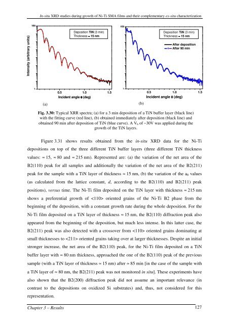
Fig. 3.30: Typical XRR spectra; (a) for a 3 min deposition of a TiN buffer layer (black line)<br />
with the fitting curve (red line), (b) obtained immediately after deposition (black line) and<br />
obtained 90 min after deposition of TiN (blue curve). A V b of −30V was applied during the<br />
growth of the TiN layers.<br />
Figure 3.31 shows results obtained from the in-situ XRD data for the Ni-Ti<br />
depositions on top of the three different TiN buffer layers (three different TiN thickness<br />
values: ≈ 15, ≈ 80 and ≈ 215 nm). Represented are: (a) the variation of the net area of the<br />
B2(110) peak for all samples and additionally the variation of the net area of the B2(211)<br />
peak for the sample with a TiN layer of thickness ≈ 15 nm, (b) the variation of the a 0 values<br />
(as calculated from the lattice constant, d, according to the B2(110) and B2(211) peak<br />
positions), versus time. The Ni-Ti film deposited on the TiN layer with thickness ≈ 215 nm<br />
shows a preferential growth of oriented grains of the Ni-Ti B2 phase from the<br />
beginning of the deposition, with a constant growth rate during the whole deposition. For the<br />
Ni-Ti film deposited on a TiN layer of thickness ≈ 15 nm, the B2(110) diffraction peak also<br />
appeared from the beginning of the deposition, but much less intense. In this latter case, the<br />
B2(211) peak was also detected with a crossover from oriented grains dominating at<br />
small thicknesses to oriented grains taking over at larger thicknesses. Despite an initial<br />
stronger increase, the net area of the B2(110) peak, for the Ni-Ti film deposited on a TiN<br />
buffer layer with ≈ 80 nm thickness, approached the one of the B2(110) peak of the previous<br />
sample (with a TiN layer of thickness ≈ 15 nm) after ≈ 85 min [in the case of the sample with<br />
a TiN layer of ≈ 80 nm, the B2(211) peak was not monitored in situ]. These experiments have<br />
also shown that the B2(200) diffraction peak did not assume an important relevance (in<br />
contrast to the depositions on oxidized Si substrates) and, thus, not considered for this<br />
representation.<br />
Chapter 3 – Results 127