PhD Thesis_RuiMSMartins.pdf - RUN UNL
PhD Thesis_RuiMSMartins.pdf - RUN UNL
PhD Thesis_RuiMSMartins.pdf - RUN UNL
Create successful ePaper yourself
Turn your PDF publications into a flip-book with our unique Google optimized e-Paper software.
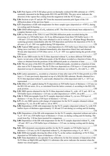
Fig. 3.25: Pole figures of Ni-Ti B2 phase grown on thermally oxidized Si(100) substrate at ≈ 470°C,<br />
nominally measured in the Bragg peaks B2(110) and B2(200). The grey arrow indicates the<br />
direction of the vapour flux coming from the magnetron with the Ni-Ti target....................... 121<br />
Fig. 3.26: Sections at ϕ = 0° and ϕ = 90° from the measured austenite pole figure of the 110<br />
diffraction plane of the previous figure. .............................................................................. 121<br />
Fig. 3.27: Dependence of ER with temperature for three sample types (deposited at ≈ 470°C), during<br />
(a) cooling and (b) heating. ................................................................................................ 123<br />
Fig. 3.28: GIXD diffractograms (Cu-K α radiation) at RT. The films had already been subjected to a<br />
complete thermal cycle. ..................................................................................................... 124<br />
Fig. 3.29: (a) Net areas of the TiN(111) and TiN(200) diffraction peaks recorded during the<br />
processing of a TiN buffer layer. (b) X-ray diffractograms from three TiN buffer layers ≈ 15,<br />
≈ 80 and ≈ 215 nm thick. They were obtained in situ in vertical, i.e. off-plane Bragg–Brentano<br />
scattering geometry immediately after the TiN deposition and before the deposition of Ni-Ti. In<br />
all cases a V b of −30V was applied during TiN deposition. .................................................. 126<br />
Fig. 3.30: Typical XRR spectra; (a) for a 3 min deposition of a TiN buffer layer (black line) with the<br />
fitting curve (red line), (b) obtained immediately after deposition (black line) and obtained<br />
90 min after deposition of TiN (blue curve). A V b of −30V was applied during the growth of the<br />
TiN layers. ....................................................................................................................... 127<br />
Fig. 3.31: In-situ XRD results for Ni-Ti films deposited without V b on three different TiN buffer<br />
layers; (a) net areas of the diffraction peaks of the B2 phase recorded as a function of time, (b) a 0<br />
values as obtained from the positions of the diffraction peaks as a function of time. .............. 128<br />
Fig. 3.32: The net areas of the B2(110) and B2(211) diffraction peaks, recorded as a function of time<br />
after start of Ni-Ti deposition. The Ni-Ti film was deposited on a TiN layer (≈ 15 nm) previously<br />
deposited on top of a thermally oxidized Si(100) substrate; (a) without V b , (b) with V b = −45V.<br />
........................................................................................................................................ 129<br />
Fig. 3.33: Lattice parameter a o , recorded as a function of time after start of Ni-Ti film growth on a TiN<br />
layer (≈ 15 nm) previously deposited on top of a SiO 2 /Si(100) substrate. Results obtained for a<br />
Ni-Ti film deposited without V b and results obtained for a film deposited with V b = −45 V are<br />
represented. ...................................................................................................................... 129<br />
Fig. 3.34: Effect of V b applied during Ni-Ti deposition on TiN buffer layers of thickness ≈ 215 nm; (a)<br />
the B2(110) net areas, (b) a o as calculated from the lattice constant, d, according to the B2(110)<br />
peak position. ................................................................................................................... 130<br />
Fig. 3.35: XRD spectra obtained for the Ni-Ti films deposited without V b , with −45 V and −90 V on<br />
TiN buffer layers of thickness ≈ 215 nm; (a) after deposition at ≈ 470°C, (b) at RT. .............. 131<br />
Fig. 3.36: X-TEM micrographs from Ni-Ti samples deposited without V b ; (a) on a TiN layer of<br />
thickness ≈ 15 nm, (b) on a TiN layer of thickness ≈ 215 nm. .............................................. 132<br />
Fig. 3.37: Ex-situ XRD spectra with change of temperature for the Ni-Ti samples obtained without<br />
applying a V b ; (a), (b) at RT and (c), (d) at 100°C. .............................................................. 133<br />
Fig. 3.38: Dependence of ER with temperature for the Ni-Ti samples (deposited without V b ) with TiN<br />
buffers layers of thickness approximately 15, 80 and 215 nm during (a) cooling and (b) heating.<br />
........................................................................................................................................ 134<br />
Fig. 3.39: Dependence of the ER with temperature for the Ni-Ti samples, deposited without and with a<br />
V b of −45 V on a TiN buffer layer of thickness ≈ 15 nm; (a) during cooling and (b) heating. The<br />
result from Fig. 3.38 has been inserted for comparison. ....................................................... 135<br />
Fig. 3.40: Dependence of the ER with temperature for the Ni-Ti samples deposited without V b , with<br />
−45 and −90 V on a TiN buffer layer of thickness ≈ 215 nm; (a) during cooling and (b) during<br />
heating. ............................................................................................................................ 135<br />
Fig. 3.41: AES elemental concentration profiles for the Ni-Ti samples on TiN buffer layers of<br />
thickness ≈ 215 nm; (a) Ni-Ti deposited without V b , (b) deposition using a V b of −90 V. ....... 136<br />
Fig. 3.42: SEM micrographs showing the effect of the V b on the surface morphology of Ni-Ti films<br />
deposited on TiN buffer layers of thickness ≈ 215 nm. ........................................................ 137<br />
Fig. 3.43: Time-dependent in-situ specular X-ray reflectivity for the first minutes of deposition of the<br />
Ni-Ti films on MgO(100) and MgO(111) substrates (the arrow indicates the moment when the<br />
shutter was closed again). .................................................................................................. 140<br />
xv


