Preliminary C8051F120/1/2/3 C8051F124/5/6/7 - KEMT FEI TUKE
Preliminary C8051F120/1/2/3 C8051F124/5/6/7 - KEMT FEI TUKE
Preliminary C8051F120/1/2/3 C8051F124/5/6/7 - KEMT FEI TUKE

You also want an ePaper? Increase the reach of your titles
YUMPU automatically turns print PDFs into web optimized ePapers that Google loves.
<strong>Preliminary</strong><br />
<strong>C8051F120</strong>/1/2/3<br />
<strong>C8051F124</strong>/5/6/7<br />
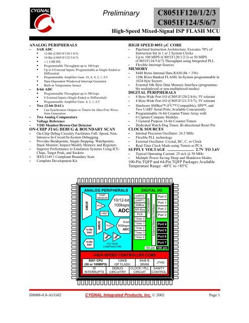
High-Speed Mixed-Signal ISP FLASH MCU<br />
ANALOG PERIPHERALS<br />
- SAR ADC<br />
• 12-Bit (<strong>C8051F120</strong>/1/4/5)<br />
• 10-Bit (C8051F122/3/6/7)<br />
• ±1LSBINL<br />
• Programmable Throughput up to 100 ksps<br />
• Up to 8 External Inputs; Programmable as Single-Ended or<br />
Differential<br />
• Programmable Amplifier Gain: 16, 8, 4, 2, 1, 0.5<br />
• Data-Dependent Windowed Interrupt Generator<br />
• Built-in Temperature Sensor<br />
- 8-bit ADC<br />
• Programmable Throughput up to 500 ksps<br />
• 8 External Inputs (Single-Ended or Differential)<br />
• Programmable Amplifier Gain: 4, 2, 1, 0.5<br />
- Two 12-bit DACs<br />
• Can Synchronize Outputs to Timers for Jitter-Free Waveform<br />
Generation<br />
- TwoAnalogComparators<br />
- Voltage Reference<br />
- VDD Monitor/Brown-Out Detector<br />
ON-CHIP JTAG DEBUG & BOUNDARY SCAN<br />
- On-Chip Debug Circuitry Facilitates Full- Speed, Non-<br />
Intrusive In-Circuit/In-System Debugging<br />
- Provides Breakpoints, Single-Stepping, Watchpoints,<br />
Stack Monitor; Inspect/Modify Memory and Registers<br />
- Superior Performance to Emulation Systems Using ICE-<br />
Chips, Target Pods, and Sockets<br />
- IEEE1149.1 Compliant Boundary Scan<br />
- Complete Development Kit<br />
HIGH SPEED 8051 µC CORE<br />
- Pipelined Instruction Architecture; Executes 70% of<br />
Instruction Set in 1 or 2 System Clocks<br />
- Up to 100 MIPS (<strong>C8051F120</strong>/1/2/3) or 50 MIPS<br />
(<strong>C8051F124</strong>/5/6/7) Throughput using Integrated PLL<br />
- Flexible Interrupt Sources<br />
MEMORY<br />
- 8448 Bytes Internal Data RAM (8k + 256)<br />
- 128k Bytes Banked FLASH; In-System programmable in<br />
1024-byte Sectors<br />
- External 64k Byte Data Memory Interface (programmable<br />
multiplexed or non-multiplexed modes)<br />
DIGITAL PERIPHERALS<br />
- 8 Byte-Wide Port I/O (<strong>C8051F120</strong>/2/4/6); 5V tolerant<br />
- 4 Byte-Wide Port I/O (C8051F121/3/5/7); 5V tolerant<br />
- Hardware SMBus (I 2 C Compatible), SPI, and<br />
Two UART Serial Ports Available Concurrently<br />
- Programmable 16-bit Counter/Timer Array with<br />
6 Capture/Compare Modules<br />
- 5 General Purpose 16-bit Counter/Timers<br />
- Dedicated Watch-Dog Timer; Bi-directional Reset Pin<br />
CLOCK SOURCES<br />
- Internal Precision Oscillator: 24.5 MHz<br />
- Flexible PLL technology<br />
- External Oscillator: Crystal, RC, C, or Clock<br />
- Real-Time Clock Mode using Timers or PCA<br />
SUPPLY VOLTAGE .......................... 2.7V TO 3.6V<br />
- Typical Operating Current: 25 mA @ 50 MHz<br />
- Multiple Power Saving Sleep and Shutdown Modes<br />
100-Pin TQFP and 64-Pin TQFP Packages Available<br />
Temperature Range: -40°C to +85°C<br />
ANALOG PERIPHERALS<br />
AMUX<br />
12-Bit<br />
DAC<br />
12-Bit<br />
DAC<br />
TEMP<br />
SENSOR<br />
PGA<br />
AMUX<br />
VREF<br />
+<br />
-<br />
PGA<br />
10/12-bit<br />
100ksps<br />
ADC<br />
+<br />
-<br />
VOLTAGE<br />
COMPARATORS<br />
8-bit<br />
500ksps<br />
ADC<br />
DIGITAL I/O<br />
UART0 Port 0<br />
UART1<br />
Port 1<br />
SMBus<br />
SPI Bus Port 2<br />
PCA<br />
Port 3<br />
Timer 0<br />
Timer 1 Port 4<br />
Timer 2<br />
Port 5<br />
Timer 3<br />
Timer 4 Port 6<br />
Port 7<br />
64 pin 100 pin<br />
CROSSBAR<br />
External Memory Interface<br />
HIGH-SPEED CONTROLLER CORE<br />
8051 CPU 128KB 8448 B<br />
(50 or 100MIPS) ISP FLASH SRAM<br />
JTAG<br />
20<br />
INTERRUPTS<br />
DEBUG<br />
CIRCUITRY<br />
CLOCK / PLL<br />
CIRCUIT<br />
SANITY<br />
CONTROL<br />
DS008-0.8-AUG02 CYGNAL Integrated Products, Inc. © 2002 Page 1
<strong>C8051F120</strong>/1/2/3<br />
<strong>C8051F124</strong>/5/6/7<br />
<strong>Preliminary</strong><br />
Notes<br />
Page 2<br />
DS008-0.8-AUG02 © 2002 Cygnal Integrated Products, Inc.
<strong>Preliminary</strong><br />
<strong>C8051F120</strong>/1/2/3<br />
<strong>C8051F124</strong>/5/6/7<br />
TABLE OF CONTENTS<br />
1. SYSTEM OVERVIEW .........................................................................................................19<br />
1.1. CIP-51 Microcontroller Core ......................................................................................25<br />
1.1.1. Fully 8051 Compatible ..........................................................................................25<br />
1.1.2. Improved Throughput ............................................................................................25<br />
1.1.3. Additional Features................................................................................................26<br />
1.2. On-Chip Memory ............................................................................................................27<br />
1.3. JTAG Debug and Boundary Scan ...................................................................................28<br />
1.4. Programmable Digital I/O and Crossbar .........................................................................29<br />
1.5. Programmable Counter Array .........................................................................................30<br />
1.6. Serial Ports.......................................................................................................................31<br />
1.7. 12-Bit Analog to Digital Converter.................................................................................32<br />
1.8. 8-Bit Analog to Digital Converter...................................................................................33<br />
1.9. Comparators and DACs...................................................................................................34<br />
2. ABSOLUTE MAXIMUM RATINGS..................................................................................35<br />
3. GLOBAL DC ELECTRICAL CHARACTERISTICS ......................................................36<br />
4. PINOUT AND PACKAGE DEFINITIONS........................................................................38<br />
5. ADC0 (12-BIT ADC, <strong>C8051F120</strong>/1/4/5 ONLY) ..................................................................47<br />
5.1. Analog Multiplexer and PGA..........................................................................................47<br />
5.2. ADC Modes of Operation ...............................................................................................49<br />
5.2.1. Starting a Conversion.............................................................................................49<br />
5.2.2. Tracking Modes .....................................................................................................50<br />
5.2.3. Settling Time Requirements ..................................................................................51<br />
5.3. ADC0 Programmable Window Detector.........................................................................58<br />
6. ADC0 (10-BIT ADC, C8051F122/3/6/7 ONLY) ..................................................................65<br />
6.1. Analog Multiplexer and PGA..........................................................................................65<br />
6.2. ADC Modes of Operation ...............................................................................................67<br />
6.2.1. Starting a Conversion.............................................................................................67<br />
6.2.2. Tracking Modes .....................................................................................................68<br />
6.2.3. Settling Time Requirements ..................................................................................69<br />
6.3. ADC0 Programmable Window Detector.........................................................................76<br />
7. ADC2 (8-BIT ADC) ...............................................................................................................83<br />
7.1. Analog Multiplexer and PGA..........................................................................................83<br />
7.2. ADC2 Modes of Operation .............................................................................................84<br />
7.2.1. Starting a Conversion.............................................................................................84<br />
7.2.2. Tracking Modes .....................................................................................................84<br />
7.2.3. Settling Time Requirements ..................................................................................86<br />
7.3. ADC2 Programmable Window Detector.........................................................................92<br />
7.3.1. Window Detector In Single-Ended Mode .............................................................92<br />
7.3.2. Window Detector In Differential Mode.................................................................93<br />
8. DACS, 12-BIT VOLTAGE MODE......................................................................................97<br />
8.1. DAC Output Scheduling..................................................................................................97<br />
8.1.1. Update Output On-Demand ...................................................................................97<br />
© 2002 Cygnal Integrated Products, Inc. DS008-0.8-AUG02 Page 3
<strong>C8051F120</strong>/1/2/3<br />
<strong>C8051F124</strong>/5/6/7<br />
<strong>Preliminary</strong><br />
8.1.2. Update Output Based on Timer Overflow.............................................................98<br />
8.2. DAC Output Scaling/Justification...................................................................................98<br />
9. VOLTAGE REFERENCE (<strong>C8051F120</strong>/2/4/6) .................................................................105<br />
10. VOLTAGE REFERENCE (C8051F121/3/5/7) .................................................................107<br />
11. COMPARATORS................................................................................................................109<br />
12. CIP-51 MICROCONTROLLER........................................................................................117<br />
12.1.Instruction Set................................................................................................................118<br />
12.1.1. Instruction and CPU Timing................................................................................118<br />
12.1.2. MOVX Instruction and Program Memory...........................................................118<br />
12.2.Memory Organization ...................................................................................................123<br />
12.2.1. Program Memory.................................................................................................123<br />
12.2.2. Data Memory .......................................................................................................125<br />
12.2.3. General Purpose Registers ...................................................................................125<br />
12.2.4. Bit Addressable Locations ...................................................................................125<br />
12.2.5. Stack .................................................................................................................125<br />
12.2.6. Special Function Registers...................................................................................126<br />
12.2.6.1.SFR Paging..................................................................................................126<br />
12.2.6.2.Interrupts and SFR Paging...........................................................................126<br />
12.2.6.3.SFR Page Stack Example ............................................................................128<br />
12.2.7. Register Descriptions...........................................................................................141<br />
12.3.Interrupt Handler ...........................................................................................................144<br />
12.3.1. MCU Interrupt Sources and Vectors ...................................................................144<br />
12.3.2. External Interrupts ...............................................................................................144<br />
12.3.3. Interrupt Priorities................................................................................................146<br />
12.3.4. Interrupt Latency..................................................................................................146<br />
12.3.5. Interrupt Register Descriptions............................................................................147<br />
12.4.Power Management Modes ...........................................................................................153<br />
12.4.1. Idle Mode.............................................................................................................153<br />
12.4.2. Stop Mode............................................................................................................153<br />
13. RESET SOURCES ..............................................................................................................155<br />
13.1.Power-on Reset..............................................................................................................156<br />
13.2.Power-fail Reset ............................................................................................................156<br />
13.3.External Reset................................................................................................................156<br />
13.4.Missing Clock Detector Reset.......................................................................................157<br />
13.5.Comparator0 Reset ........................................................................................................157<br />
13.6.External CNVSTR0 Pin Reset.......................................................................................157<br />
13.7.Watchdog Timer Reset..................................................................................................157<br />
13.7.1. Enable/Reset WDT ..............................................................................................157<br />
13.7.2. Disable WDT .......................................................................................................158<br />
13.7.3. Disable WDT Lockout.........................................................................................158<br />
13.7.4. Setting WDT Interval...........................................................................................158<br />
14. OSCILLATORS...................................................................................................................161<br />
14.1.Programmable Internal Oscillator .................................................................................161<br />
14.2.External Oscillator Drive Circuit...................................................................................163<br />
14.3.System Clock Selection.................................................................................................163<br />
Page 4<br />
DS008-0.8-AUG02 © 2002 Cygnal Integrated Products, Inc.
<strong>Preliminary</strong><br />
<strong>C8051F120</strong>/1/2/3<br />
<strong>C8051F124</strong>/5/6/7<br />
14.4.External Crystal Example..............................................................................................166<br />
14.5.External RC Example....................................................................................................166<br />
14.6.External Capacitor Example..........................................................................................166<br />
14.7.Phase-Locked Loop (PLL) ............................................................................................167<br />
14.7.1. PLL Input Clock and Pre-divider.........................................................................167<br />
14.7.2. PLL Multiplication and Output Clock .................................................................167<br />
14.7.3. Powering on and Initializing the PLL..................................................................168<br />
15. FLASH MEMORY ..............................................................................................................173<br />
15.1.Programming The Flash Memory .................................................................................173<br />
15.1.1. Non-volatile Data Storage ...................................................................................173<br />
15.1.2. Erasing FLASH Pages From Software ................................................................174<br />
15.1.3. Writing FLASH Memory From Software ...........................................................175<br />
15.2.Security Options ............................................................................................................176<br />
16. BRANCH TARGET CACHE.............................................................................................181<br />
16.1.Cache and Prefetch Operation.......................................................................................181<br />
16.2.Cache and Prefetch Optimization..................................................................................182<br />
17. EXTERNAL DATA MEMORY INTERFACE AND ON-CHIP XRAM.......................187<br />
17.1.Accessing XRAM..........................................................................................................187<br />
17.1.1. 16-Bit MOVX Example.......................................................................................187<br />
17.1.2. 8-Bit MOVX Example.........................................................................................187<br />
17.2.Configuring the External Memory Interface .................................................................187<br />
17.3.Port Selection and Configuration ..................................................................................188<br />
17.4.Multiplexed and Non-multiplexed Selection.................................................................190<br />
17.4.1. Multiplexed Configuration ..................................................................................190<br />
17.4.2. Non-multiplexed Configuration...........................................................................191<br />
17.5.Memory Mode Selection ...............................................................................................192<br />
17.5.1. Internal XRAM Only ...........................................................................................192<br />
17.5.2. Split Mode without Bank Select ..........................................................................192<br />
17.5.3. Split Mode with Bank Select ...............................................................................193<br />
17.5.4. External Only.......................................................................................................193<br />
17.6.Timing .......................................................................................................................194<br />
17.6.1. Non-multiplexed Mode........................................................................................195<br />
17.6.1.1.16-bit MOVX: EMI0CF[4:2] = ‘101’, ‘110’, or ‘111’................................195<br />
17.6.1.2.8-bit MOVX without Bank Select: EMI0CF[4:2] = ‘101’ or ‘111’............196<br />
17.6.1.3.8-bit MOVX with Bank Select: EMI0CF[4:2] = ‘110’...............................197<br />
17.6.2. Multiplexed Mode................................................................................................198<br />
17.6.2.1.16-bit MOVX: EMI0CF[4:2] = ‘001’, ‘010’, or ‘011’................................198<br />
17.6.2.2.8-bit MOVX without Bank Select: EMI0CF[4:2] = ‘001’ or ‘011’............199<br />
17.6.2.3.8-bit MOVX with Bank Select: EMI0CF[4:2] = ‘010’...............................200<br />
18. PORT INPUT/OUTPUT .....................................................................................................203<br />
18.1.Ports 0 through 3 and the Priority Crossbar Decoder....................................................205<br />
18.1.1. Crossbar Pin Assignment and Allocation ............................................................205<br />
18.1.2. Configuring the Output Modes of the Port Pins ..................................................206<br />
18.1.3. Configuring Port Pins as Digital Inputs...............................................................207<br />
18.1.4. Weak Pull-ups......................................................................................................207<br />
© 2002 Cygnal Integrated Products, Inc. DS008-0.8-AUG02 Page 5
<strong>C8051F120</strong>/1/2/3<br />
<strong>C8051F124</strong>/5/6/7<br />
<strong>Preliminary</strong><br />
18.1.5. Configuring Port 1 Pins as Analog Inputs ...........................................................207<br />
18.1.6. External Memory Interface Pin Assignments......................................................208<br />
18.1.7. Crossbar Pin Assignment Example......................................................................210<br />
18.2.Ports 4 through 7 (<strong>C8051F120</strong>/2/4/6 only) ...................................................................219<br />
18.2.1. Configuring Ports which are not Pinned Out.......................................................219<br />
18.2.2. Configuring the Output Modes of the Port Pins ..................................................219<br />
18.2.3. Configuring Port Pins as Digital Inputs...............................................................220<br />
18.2.4. Weak Pull-ups......................................................................................................220<br />
18.2.5. External Memory Interface..................................................................................220<br />
19. SYSTEM MANAGEMENT BUS / I2C BUS (SMBUS0) .................................................225<br />
19.1.Supporting Documents ..................................................................................................227<br />
19.2.SMBus Protocol.............................................................................................................227<br />
19.2.1. Arbitration............................................................................................................227<br />
19.2.2. Clock Low Extension...........................................................................................228<br />
19.2.3. SCL Low Timeout ...............................................................................................228<br />
19.2.4. SCL High (SMBus Free) Timeout.......................................................................228<br />
19.3.SMBus Transfer Modes.................................................................................................229<br />
19.3.1. Master Transmitter Mode ....................................................................................229<br />
19.3.2. Master Receiver Mode.........................................................................................229<br />
19.3.3. Slave Transmitter Mode.......................................................................................230<br />
19.3.4. Slave Receiver Mode ...........................................................................................230<br />
19.4.SMBus Special Function Registers ...............................................................................231<br />
19.4.1. Control Register...................................................................................................231<br />
19.4.2. Clock Rate Register .............................................................................................233<br />
19.4.3. Data Register........................................................................................................234<br />
19.4.4. Address Register ..................................................................................................234<br />
19.4.5. Status Register .....................................................................................................235<br />
20. ENHANCED SERIAL PERIPHERAL INTERFACE (SPI0) .........................................239<br />
20.1.Signal Descriptions........................................................................................................240<br />
20.1.1. Master Out, Slave In (MOSI) ..............................................................................240<br />
20.1.2. Master In, Slave Out (MISO) ..............................................................................240<br />
20.1.3. Serial Clock (SCK) ..............................................................................................240<br />
20.1.4. Slave Select (NSS)...............................................................................................240<br />
20.2.SPI0 Master Mode Operation........................................................................................241<br />
20.3.SPI0 Slave Mode Operation ..........................................................................................243<br />
20.4.SPI0 Interrupt Sources...................................................................................................244<br />
20.5.Serial Clock Timing ......................................................................................................245<br />
20.6.SPISpecial Function Registers .....................................................................................246<br />
21. UART0 ..................................................................................................................................253<br />
21.1.UART0 Operational Modes ..........................................................................................254<br />
21.1.1. Mode 0: Synchronous Mode................................................................................254<br />
21.1.2. Mode 1: 8-Bit UART, Variable Baud Rate .........................................................255<br />
21.1.3. Mode 2: 9-Bit UART, Fixed Baud Rate ..............................................................256<br />
21.1.4. Mode 3: 9-Bit UART, Variable Baud Rate .........................................................257<br />
21.2.Multiprocessor Communications...................................................................................258<br />
Page 6<br />
DS008-0.8-AUG02 © 2002 Cygnal Integrated Products, Inc.
<strong>Preliminary</strong><br />
<strong>C8051F120</strong>/1/2/3<br />
<strong>C8051F124</strong>/5/6/7<br />
21.2.1. Configuration of a Masked Address ....................................................................258<br />
21.2.2. Broadcast Addressing ..........................................................................................258<br />
21.3.Frame and Transmission Error Detection......................................................................259<br />
22. UART1 ..................................................................................................................................265<br />
22.1.Enhanced Baud Rate Generation...................................................................................266<br />
22.2.Operational Modes ........................................................................................................267<br />
22.2.1. 8-Bit UART .........................................................................................................267<br />
22.2.2. 9-Bit UART .........................................................................................................268<br />
22.3.Multiprocessor Communications...................................................................................269<br />
23. TIMERS................................................................................................................................275<br />
23.1.Timer 0 and Timer 1......................................................................................................275<br />
23.1.1. Mode 0: 13-bit Counter/Timer.............................................................................275<br />
23.1.2. Mode 1: 16-bit Counter/Timer.............................................................................276<br />
23.1.3. Mode 2: 8-bit Counter/Timer with Auto-Reload.................................................277<br />
23.1.4. Mode 3: Two 8-bit Counter/Timers (Timer 0 Only) ...........................................278<br />
23.2.Timer 2, Timer 3, and Timer 4......................................................................................283<br />
23.2.1. Configuring Timer 2, 3, and 4 to Count Down....................................................283<br />
23.2.2. Capture Mode ......................................................................................................284<br />
23.2.3. Auto-Reload Mode ..............................................................................................285<br />
23.2.4. Toggle Output Mode (Timer 2 and Timer 4 Only)..............................................285<br />
24. PROGRAMMABLE COUNTER ARRAY .......................................................................291<br />
24.1.PCA Counter/Timer.......................................................................................................292<br />
24.2.Capture/Compare Modules............................................................................................293<br />
24.2.1. Edge-triggered Capture Mode .............................................................................294<br />
24.2.2. Software Timer (Compare) Mode........................................................................295<br />
24.2.3. High Speed Output Mode ....................................................................................296<br />
24.2.4. Frequency Output Mode ......................................................................................297<br />
24.2.5. 8-Bit Pulse Width Modulator Mode ....................................................................298<br />
24.2.6. 16-Bit Pulse Width Modulator Mode ..................................................................299<br />
24.3.Register Descriptions for PCA0 ....................................................................................300<br />
25. JTAG (IEEE 1149.1)............................................................................................................305<br />
25.1.Boundary Scan...............................................................................................................306<br />
25.1.1. EXTEST Instruction ............................................................................................307<br />
25.1.2. SAMPLE Instruction ...........................................................................................307<br />
25.1.3. BYPASS Instruction ............................................................................................307<br />
25.1.4. IDCODE Instruction ............................................................................................307<br />
25.2.Flash Programming Commands ....................................................................................308<br />
25.3.Debug Support...............................................................................................................312<br />
© 2002 Cygnal Integrated Products, Inc. DS008-0.8-AUG02 Page 7
<strong>C8051F120</strong>/1/2/3<br />
<strong>C8051F124</strong>/5/6/7<br />
<strong>Preliminary</strong><br />
Notes<br />
Page 8<br />
DS008-0.8-AUG02 © 2002 Cygnal Integrated Products, Inc.
<strong>Preliminary</strong><br />
<strong>C8051F120</strong>/1/2/3<br />
<strong>C8051F124</strong>/5/6/7<br />
LIST OF FIGURES<br />
1. SYSTEM OVERVIEW .........................................................................................................19<br />
Figure 1.1. <strong>C8051F120</strong>/124 Block Diagram..........................................................................21<br />
Figure 1.2. C8051F121/125 Block Diagram..........................................................................22<br />
Figure 1.3. C8051F122/126 Block Diagram..........................................................................23<br />
Figure 1.4. C8051F123/127 Block Diagram..........................................................................24<br />
Figure 1.5. On-Board Clock and Reset..................................................................................26<br />
Figure 1.6. On-Chip Memory Map........................................................................................27<br />
Figure 1.7. Development/In-System Debug Diagram ...........................................................28<br />
Figure 1.8. Digital Crossbar Diagram....................................................................................29<br />
Figure 1.9. PCA Block Diagram............................................................................................30<br />
Figure 1.10. 12-Bit ADC Block Diagram................................................................................32<br />
Figure 1.11. 8-Bit ADC Diagram ............................................................................................33<br />
Figure 1.12. Comparator and DAC Diagram...........................................................................34<br />
2. ABSOLUTE MAXIMUM RATINGS..................................................................................35<br />
3. GLOBAL DC ELECTRICAL CHARACTERISTICS ......................................................36<br />
4. PINOUT AND PACKAGE DEFINITIONS........................................................................38<br />
Figure 4.1. TQFP-100 Pinout Diagram..................................................................................43<br />
Figure 4.2. TQFP-100 Package Drawing...............................................................................44<br />
Figure 4.3. TQFP-64 Pinout Diagram....................................................................................45<br />
Figure 4.4. TQFP-64 Package Drawing.................................................................................46<br />
5. ADC0 (12-BIT ADC, <strong>C8051F120</strong>/1/4/5 ONLY) ..................................................................47<br />
Figure 5.1. 12-Bit ADC0 Functional Block Diagram............................................................47<br />
Figure 5.2. Typical Temperature Sensor Transfer Function..................................................48<br />
Figure 5.3. ADC0 Track and Conversion Example Timing ..................................................50<br />
Figure 5.4. ADC0 Equivalent Input Circuits .........................................................................51<br />
Figure 5.5. AMX0CF: AMUX0 Configuration Register.......................................................52<br />
Figure 5.6. AMX0SL: AMUX0 Channel Select Register .....................................................53<br />
Figure 5.7. ADC0CF: ADC0 Configuration Register ...........................................................54<br />
Figure 5.8. ADC0CN: ADC0 Control Register.....................................................................55<br />
Figure 5.9. ADC0H: ADC0 Data Word MSB Register.........................................................56<br />
Figure 5.10. ADC0L: ADC0 Data Word LSB Register ..........................................................56<br />
Figure 5.11. ADC0 Data Word Example.................................................................................57<br />
Figure 5.12. ADC0GTH: ADC0 Greater-Than Data High Byte Register...............................58<br />
Figure 5.13. ADC0GTL: ADC0 Greater-Than Data Low Byte Register................................58<br />
Figure 5.14. ADC0LTH: ADC0 Less-Than Data High Byte Register....................................59<br />
Figure 5.15. ADC0LTL: ADC0 Less-Than Data Low Byte Register .....................................59<br />
Figure 5.16. 12-Bit ADC0 Window Interrupt Example: Right Justified Single-Ended Data .60<br />
Figure 5.17. 12-Bit ADC0 Window Interrupt Example: Right Justified Differential Data.....61<br />
Figure 5.18. 12-Bit ADC0 Window Interrupt Example: Left Justified Single-Ended Data....62<br />
Figure 5.19. 12-Bit ADC0 Window Interrupt Example: Left Justified Differential Data.......63<br />
6. ADC0 (10-BIT ADC, C8051F122/3/6/7 ONLY) ..................................................................65<br />
Figure 6.1. 10-Bit ADC0 Functional Block Diagram............................................................65<br />
© 2002 Cygnal Integrated Products, Inc. DS008-0.8-AUG02 Page 9
<strong>C8051F120</strong>/1/2/3<br />
<strong>C8051F124</strong>/5/6/7<br />
<strong>Preliminary</strong><br />
Figure 6.2. Typical Temperature Sensor Transfer Function..................................................66<br />
Figure 6.3. ADC0 Track and Conversion Example Timing ..................................................68<br />
Figure 6.4. ADC0 Equivalent Input Circuits .........................................................................69<br />
Figure 6.5. AMX0CF: AMUX0 Configuration Register.......................................................70<br />
Figure 6.6. AMX0SL: AMUX0 Channel Select Register .....................................................71<br />
Figure 6.7. ADC0CF: ADC0 Configuration Register ...........................................................72<br />
Figure 6.8. ADC0CN: ADC0 Control Register.....................................................................73<br />
Figure 6.9. ADC0H: ADC0 Data Word MSB Register.........................................................74<br />
Figure 6.10. ADC0L: ADC0 Data Word LSB Register ..........................................................74<br />
Figure 6.11. ADC0 Data Word Example.................................................................................75<br />
Figure 6.12. ADC0GTH: ADC0 Greater-Than Data High Byte Register...............................76<br />
Figure 6.13. ADC0GTL: ADC0 Greater-Than Data Low Byte Register................................76<br />
Figure 6.14. ADC0LTH: ADC0 Less-Than Data High Byte Register....................................77<br />
Figure 6.15. ADC0LTL: ADC0 Less-Than Data Low Byte Register .....................................77<br />
Figure 6.16. 10-Bit ADC0 Window Interrupt Example: Right Justified Single-Ended Data .78<br />
Figure 6.17. 10-Bit ADC0 Window Interrupt Example: Right Justified Differential Data.....79<br />
Figure 6.18. 10-Bit ADC0 Window Interrupt Example: Left Justified Single-Ended Data....80<br />
Figure 6.19. 10-Bit ADC0 Window Interrupt Example: Left Justified Differential Data.......81<br />
7. ADC2 (8-BIT ADC) ...............................................................................................................83<br />
Figure 7.1. ADC2 Functional Block Diagram.......................................................................83<br />
Figure 7.2. ADC2 Track and Conversion Example Timing ..................................................85<br />
Figure 7.3. ADC2 Equivalent Input Circuit...........................................................................86<br />
Figure 7.4. AMX2CF: AMUX2 Configuration Register.......................................................87<br />
Figure 7.5. AMX2SL: AMUX2 Channel Select Register .....................................................88<br />
Figure 7.6. ADC2CF: ADC2 Configuration Register ...........................................................89<br />
Figure 7.7. ADC2CN: ADC2 Control Register.....................................................................90<br />
Figure 7.8. ADC2: ADC2 Data Word Register .....................................................................91<br />
Figure 7.9. ADC2 Data Word Example.................................................................................91<br />
Figure 7.10. ADC2 Window Compare Examples, Single-Ended Mode .................................92<br />
Figure 7.11. ADC2 Window Compare Examples, Differential Mode ....................................93<br />
Figure 7.12. ADC2GT: ADC2 Greater-Than Data Byte Register...........................................94<br />
Figure 7.13. ADC2LT: ADC2 Less-Than Data Byte Register................................................94<br />
8. DACS, 12-BIT VOLTAGE MODE......................................................................................97<br />
Figure 8.1. DAC Functional Block Diagram.........................................................................97<br />
Figure 8.2. DAC0H: DAC0 High Byte Register ...................................................................99<br />
Figure 8.3. DAC0L: DAC0 Low Byte Register ....................................................................99<br />
Figure 8.4. DAC0CN: DAC0 Control Register...................................................................100<br />
Figure 8.5. DAC1H: DAC1 High Byte Register .................................................................101<br />
Figure 8.6. DAC1L: DAC1 Low Byte Register ..................................................................101<br />
Figure 8.7. DAC1CN: DAC1 Control Register...................................................................102<br />
9. VOLTAGE REFERENCE (<strong>C8051F120</strong>/2/4/6) .................................................................105<br />
Figure 9.1. Voltage Reference Functional Block Diagram..................................................105<br />
Figure 9.2. REF0CN: Reference Control Register ..............................................................106<br />
10. VOLTAGE REFERENCE (C8051F121/3/5/7) .................................................................107<br />
Figure 10.1. Voltage Reference Functional Block Diagram .................................................107<br />
Page 10<br />
DS008-0.8-AUG02 © 2002 Cygnal Integrated Products, Inc.
<strong>Preliminary</strong><br />
<strong>C8051F120</strong>/1/2/3<br />
<strong>C8051F124</strong>/5/6/7<br />
Figure 10.2. REF0CN: Reference Control Register ..............................................................108<br />
11. COMPARATORS................................................................................................................109<br />
Figure 11.1. Comparator Functional Block Diagram ............................................................109<br />
Figure 11.2. Comparator Hysteresis Plot...............................................................................111<br />
Figure 11.3. CPT0CN: Comparator0 Control Register .........................................................112<br />
Figure 11.4. CPT0MD: Comparator0 Mode Selection Register ...........................................113<br />
Figure 11.5. CPT1CN: Comparator1 Control Register .........................................................114<br />
Figure 11.6. CPT1MD: Comparator1 Mode Selection Register ...........................................115<br />
12. CIP-51 MICROCONTROLLER........................................................................................117<br />
Figure 12.1. CIP-51 Block Diagram.....................................................................................117<br />
Figure 12.2. Memory Map.....................................................................................................123<br />
Figure 12.3. PSBANK: Program Space Bank Select Register ..............................................124<br />
Figure 12.4. Address Memory Map for Instruction Fetches..................................................124<br />
Figure 12.5. SFR Page Stack .................................................................................................127<br />
Figure 12.6. SFR Page Stack While Using SFR Page 0x0F To Access Port 5 .....................128<br />
Figure 12.7. SFR Page Stack After ADC2 Window Comparator Interrupt Occurs ..............129<br />
Figure 12.8. SFR Page Stack Upon PCA Interrupt Occurring During an ADC2 ISR...........130<br />
Figure 12.9. SFR Page Stack Upon Return From PCA Interrupt ..........................................131<br />
Figure 12.10. SFR Page Stack Upon Return From ADC2 Window Interrupt.......................132<br />
Figure 12.11. SFRPGCN: SFR Page Control Register..........................................................133<br />
Figure 12.12. SFRPAGE: SFR Page Register .......................................................................133<br />
Figure 12.13. SFRNEXT: SFR Next Register.......................................................................134<br />
Figure 12.14. SFRLAST: SFR Last Register ........................................................................134<br />
Figure 12.15. SP: Stack Pointer .............................................................................................141<br />
Figure 12.16. DPL: Data Pointer Low Byte ..........................................................................141<br />
Figure 12.17. DPH: Data Pointer High Byte .........................................................................141<br />
Figure 12.18. PSW: Program Status Word ............................................................................142<br />
Figure 12.19. ACC: Accumulator..........................................................................................143<br />
Figure 12.20. B: B Register ...................................................................................................143<br />
Figure 12.21. IE: Interrupt Enable .........................................................................................147<br />
Figure 12.22. IP: Interrupt Priority ........................................................................................148<br />
Figure 12.23. EIE1: Extended Interrupt Enable 1 .................................................................149<br />
Figure 12.24. EIE2: Extended Interrupt Enable 2 .................................................................150<br />
Figure 12.25. EIP1: Extended Interrupt Priority 1.................................................................151<br />
Figure 12.26. EIP2: Extended Interrupt Priority 2.................................................................152<br />
Figure 12.27. PCON: Power Control.....................................................................................154<br />
13. RESET SOURCES ..............................................................................................................155<br />
Figure 13.1. Reset Sources ....................................................................................................155<br />
Figure 13.2. Reset Timing .....................................................................................................156<br />
Figure 13.3. WDTCN: Watchdog Timer Control Register ...................................................158<br />
Figure 13.4. RSTSRC: Reset Source Register.......................................................................159<br />
14. OSCILLATORS...................................................................................................................161<br />
Figure 14.1. Oscillator Diagram ............................................................................................161<br />
Figure 14.2. OSCICL: Internal Oscillator Calibration Register ............................................162<br />
Figure 14.3. OSCICN: Internal Oscillator Control Register .................................................162<br />
© 2002 Cygnal Integrated Products, Inc. DS008-0.8-AUG02 Page 11
<strong>C8051F120</strong>/1/2/3<br />
<strong>C8051F124</strong>/5/6/7<br />
<strong>Preliminary</strong><br />
Figure 14.4. CLKSEL: System Clock Selection Register .....................................................164<br />
Figure 14.5. OSCXCN: External Oscillator Control Register...............................................165<br />
Figure 14.6. PLL Block Diagram ..........................................................................................167<br />
Figure 14.7. PLL0CN: PLL Control Register........................................................................169<br />
Figure 14.8. PLL0DIV: PLL Pre-divider Register ................................................................169<br />
Figure 14.9. PLL0MUL: PLL Clock Scaler Register............................................................170<br />
Figure 14.10. PLL0FLT: PLL Filter Register........................................................................170<br />
15. FLASH MEMORY ..............................................................................................................173<br />
Figure 15.1. FLASH Memory Map for MOVC Read and MOVX Write Operations...........174<br />
Figure 15.2. FLASH Program Memory Map and Security Bytes .........................................177<br />
Figure 15.3. FLACL: FLASH Access Limit .........................................................................178<br />
Figure 15.4. FLSCL: FLASH Memory Control ....................................................................179<br />
Figure 15.5. PSCTL: Program Store Read/Write Control .....................................................180<br />
16. BRANCH TARGET CACHE.............................................................................................181<br />
Figure 16.1. Branch Target Cache Data Flow .......................................................................181<br />
Figure 16.2. Branch Target Cache Organiztion.....................................................................182<br />
Figure 16.3. Cache Lock Operation.......................................................................................183<br />
Figure 16.4. CCH0CN: Cache Control Register....................................................................184<br />
Figure 16.5. CCH0TN: Cache Tuning Register ....................................................................185<br />
Figure 16.6. CCH0LC: Cache Lock Control Register...........................................................185<br />
Figure 16.7. CCH0MA: Cache Miss Accumulator................................................................186<br />
Figure 16.8. FLSTAT: FLASH Status...................................................................................186<br />
17. EXTERNAL DATA MEMORY INTERFACE AND ON-CHIP XRAM.......................187<br />
Figure 17.1. EMI0CN: External Memory Interface Control .................................................189<br />
Figure 17.2. EMI0CF: External Memory Configuration.......................................................189<br />
Figure 17.3. Multiplexed Configuration Example.................................................................190<br />
Figure 17.4. Non-multiplexed Configuration Example .........................................................191<br />
Figure 17.5. EMIF Operating Modes.....................................................................................192<br />
Figure 17.6. EMI0TC: External Memory Timing Control ....................................................194<br />
Figure 17.7. Non-multiplexed 16-bit MOVX Timing ...........................................................195<br />
Figure 17.8. Non-multiplexed 8-bit MOVX without Bank Select Timing............................196<br />
Figure 17.9. Non-multiplexed 8-bit MOVX with Bank Select Timing.................................197<br />
Figure 17.10. Multiplexed 16-bit MOVX Timing.................................................................198<br />
Figure 17.11. Multiplexed 8-bit MOVX without Bank Select Timing .................................199<br />
Figure 17.12. Multiplexed 8-bit MOVX with Bank Select Timing.......................................200<br />
18. PORT INPUT/OUTPUT .....................................................................................................203<br />
Figure 18.1. Port I/O Cell Block Diagram.............................................................................203<br />
Figure 18.2. Port I/O Functional Block Diagram ..................................................................204<br />
Figure 18.3. Priority Crossbar Decode Table ........................................................................205<br />
Figure 18.4. Priority Crossbar Decode Table ........................................................................208<br />
Figure 18.5. Priority Crossbar Decode Table ........................................................................209<br />
Figure 18.6. Crossbar Example: ............................................................................................211<br />
Figure 18.7. XBR0: Port I/O Crossbar Register 0 .................................................................212<br />
Figure 18.8. XBR1: Port I/O Crossbar Register 1 .................................................................213<br />
Figure 18.9. XBR2: Port I/O Crossbar Register 2 .................................................................214<br />
Page 12<br />
DS008-0.8-AUG02 © 2002 Cygnal Integrated Products, Inc.
<strong>Preliminary</strong><br />
<strong>C8051F120</strong>/1/2/3<br />
<strong>C8051F124</strong>/5/6/7<br />
Figure 18.10. P0: Port0 Data Register ...................................................................................215<br />
Figure 18.11. P0MDOUT: Port0 Output Mode Register.......................................................215<br />
Figure 18.12. P1: Port1 Data Register ...................................................................................216<br />
Figure 18.13. P1MDIN: Port1 Input Mode Register .............................................................216<br />
Figure 18.14. P1MDOUT: Port1 Output Mode Register.......................................................217<br />
Figure 18.15. P2: Port2 Data Register ...................................................................................217<br />
Figure 18.16. P2MDOUT: Port2 Output Mode Register.......................................................218<br />
Figure 18.17. P3: Port3 Data Register ...................................................................................218<br />
Figure 18.18. P3MDOUT: Port3 Output Mode Register.......................................................219<br />
Figure 18.19. P4: Port4 Data Register ...................................................................................221<br />
Figure 18.20. P4MDOUT: Port4 Output Mode Register.......................................................221<br />
Figure 18.21. P5: Port5 Data Register ...................................................................................222<br />
Figure 18.22. P5MDOUT: Port5 Output Mode Register.......................................................222<br />
Figure 18.23. P6: Port6 Data Register ...................................................................................223<br />
Figure 18.24. P6MDOUT: Port6 Output Mode Register.......................................................223<br />
Figure 18.25. P7: Port7 Data Register ...................................................................................224<br />
Figure 18.26. P7MDOUT: Port7 Output Mode Register.......................................................224<br />
19. SYSTEM MANAGEMENT BUS / I2C BUS (SMBUS0) .................................................225<br />
Figure 19.1. SMBus0 Block Diagram ...................................................................................225<br />
Figure 19.2. Typical SMBus Configuration ..........................................................................226<br />
Figure 19.3. SMBus Transaction ...........................................................................................227<br />
Figure 19.4. Typical Master Transmitter Sequence...............................................................229<br />
Figure 19.5. Typical Master Receiver Sequence ...................................................................229<br />
Figure 19.6. Typical Slave Transmitter Sequence.................................................................230<br />
Figure 19.7. Typical Slave Receiver Sequence .....................................................................230<br />
Figure 19.8. SMB0CN: SMBus0 Control Register ...............................................................232<br />
Figure 19.9. SMB0CR: SMBus0 Clock Rate Register..........................................................233<br />
Figure 19.10. SMB0DAT: SMBus0 Data Register ...............................................................234<br />
Figure 19.11. SMB0ADR: SMBus0 Address Register..........................................................234<br />
Figure 19.12. SMB0STA: SMBus0 Status Register..............................................................235<br />
20. ENHANCED SERIAL PERIPHERAL INTERFACE (SPI0) .........................................239<br />
Figure 20.1. SPIBlock Diagram............................................................................................239<br />
Figure 20.2. Multiple-Master Mode Connection Diagram ....................................................242<br />
Figure 20.3. 3-Wire Single Master and 3-Wire Single Slave Mode Connection Diagram ...242<br />
Figure 20.4. 4-Wire Single Master Mode and 4-Wire Slave Mode Connection Diagram ....242<br />
Figure 20.5. Data/Clock Timing Diagram .............................................................................245<br />
Figure 20.6. SPI0CFG: SPI0 Configuration Register............................................................246<br />
Figure 20.7. SPI0CN: SPI0 Control Register ........................................................................247<br />
Figure 20.8. SPI0CKR: SPI0 Clock Rate Register................................................................248<br />
Figure 20.9. SPI0DAT: SPI0 Data Register ..........................................................................249<br />
Figure 20.10. SPISlave Timing (Mode 0 and Mode 2) ........................................................250<br />
Figure 20.11. SPISlave Timing (Mode 1 and Mode 3) ........................................................250<br />
21. UART0 ..................................................................................................................................253<br />
Figure 21.1. UART0 Block Diagram.....................................................................................253<br />
Figure 21.2. UART0 Mode 0 Timing Diagram .....................................................................254<br />
© 2002 Cygnal Integrated Products, Inc. DS008-0.8-AUG02 Page 13
<strong>C8051F120</strong>/1/2/3<br />
<strong>C8051F124</strong>/5/6/7<br />
<strong>Preliminary</strong><br />
Figure 21.3. UART0 Mode 0 Interconnect............................................................................254<br />
Figure 21.4. UART0 Mode 1 Timing Diagram .....................................................................255<br />
Figure 21.5. UART0 Modes 2 and 3 Timing Diagram..........................................................256<br />
Figure 21.6. UART0 Modes 1, 2, and 3 Interconnect Diagram ............................................257<br />
Figure 21.7. UART Multi-Processor Mode Interconnect Diagram .......................................259<br />
Figure 21.8. SCON0: UART0 Control Register....................................................................261<br />
Figure 21.9. SSTA0: UART0 Status and Clock Selection Register......................................262<br />
Figure 21.10. SBUF0: UART0 Data Buffer Register............................................................263<br />
Figure 21.11. SADDR0: UART0 Slave Address Register ....................................................263<br />
Figure 21.12. SADEN0: UART0 Slave Address Enable Register ........................................263<br />
22. UART1 ..................................................................................................................................265<br />
Figure 22.1. UART1 Block Diagram.....................................................................................265<br />
Figure 22.2. UART1 Baud Rate Logic ..................................................................................266<br />
Figure 22.3. UART Interconnect Diagram ............................................................................267<br />
Figure 22.4. 8-Bit UART Timing Diagram ...........................................................................267<br />
Figure 22.5. 9-Bit UART Timing Diagram ...........................................................................268<br />
Figure 22.6. UART Multi-Processor Mode Interconnect Diagram .......................................269<br />
Figure 22.7. SCON1: Serial Port 1 Control Register.............................................................270<br />
Figure 22.8. SBUF1: Serial (UART1) Port Data Buffer Register .........................................271<br />
23. TIMERS................................................................................................................................275<br />
Figure 23.1. T0 Mode 0 Block Diagram................................................................................276<br />
Figure 23.2. T0 Mode 2 Block Diagram................................................................................277<br />
Figure 23.3. T0 Mode 3 Block Diagram................................................................................278<br />
Figure 23.4. TCON: Timer Control Register.........................................................................279<br />
Figure 23.5. TMOD: Timer Mode Register...........................................................................280<br />
Figure 23.6. CKCON: Clock Control Register......................................................................281<br />
Figure 23.7. TL0: Timer 0 Low Byte ....................................................................................282<br />
Figure 23.8. TL1: Timer 1 Low Byte ....................................................................................282<br />
Figure 23.9. TH0: Timer 0 High Byte ...................................................................................282<br />
Figure 23.10. TH1: Timer 1 High Byte .................................................................................282<br />
Figure 23.11. T2, 3, and 4 Capture Mode Block Diagram ....................................................284<br />
Figure 23.12. T2, 3, and 4 Auto-reload Mode Block Diagram..............................................285<br />
Figure 23.13. TMRnCN: Timer 2, 3, and 4 Control Registers ..............................................287<br />
Figure 23.14. TMRnCF: Timer 2, 3, and 4 Configuration Registers ....................................288<br />
Figure 23.15. RCAPnL: Timer 2, 3, and 4 Capture Register Low Byte................................289<br />
Figure 23.16. RCAPnH: Timer 2, 3, and 4 Capture Register High Byte ..............................289<br />
Figure 23.17. TMRnL: Timer 2, 3, and 4 Low Byte .............................................................289<br />
Figure 23.18. TMRnH Timer 2, 3, and 4 High Byte .............................................................290<br />
24. PROGRAMMABLE COUNTER ARRAY .......................................................................291<br />
Figure 24.1. PCA Block Diagram..........................................................................................291<br />
Figure 24.2. PCA Counter/Timer Block Diagram.................................................................292<br />
Figure 24.3. PCA Interrupt Block Diagram...........................................................................293<br />
Figure 24.4. PCA Capture Mode Diagram ............................................................................294<br />
Figure 24.5. PCA Software Timer Mode Diagram................................................................295<br />
Figure 24.6. PCA High Speed Output Mode Diagram ..........................................................296<br />
Page 14<br />
DS008-0.8-AUG02 © 2002 Cygnal Integrated Products, Inc.
<strong>Preliminary</strong><br />
<strong>C8051F120</strong>/1/2/3<br />
<strong>C8051F124</strong>/5/6/7<br />
Figure 24.7. PCA Frequency Output Mode...........................................................................297<br />
Figure 24.8. PCA 8-Bit PWM Mode Diagram ......................................................................298<br />
Figure 24.9. PCA 16-Bit PWM Mode ...................................................................................299<br />
Figure 24.10. PCA0CN: PCA Control Register ....................................................................300<br />
Figure 24.11. PCA0MD: PCA0 Mode Register ....................................................................301<br />
Figure 24.12. PCA0CPMn: PCA0 Capture/Compare Mode Registers .................................302<br />
Figure 24.13. PCA0L: PCA0 Counter/Timer Low Byte .......................................................303<br />
Figure 24.14. PCA0H: PCA0 Counter/Timer High Byte ......................................................303<br />
Figure 24.15. PCA0CPLn: PCA0 Capture Module Low Byte ..............................................304<br />
Figure 24.16. PCA0CPHn: PCA0 Capture Module High Byte.............................................304<br />
25. JTAG (IEEE 1149.1)............................................................................................................305<br />
Figure 25.1. IR: JTAG Instruction Register ..........................................................................305<br />
Figure 25.2. DEVICEID: JTAG Device ID Register ............................................................307<br />
Figure 25.3. FLASHCON: JTAG Flash Control Register.....................................................309<br />
Figure 25.4. FLASHDAT: JTAG Flash Data Register..........................................................310<br />
Figure 25.5. FLASHADR: JTAG Flash Address Register....................................................310<br />
Figure 25.6. FLASHSCL: JTAG Flash Scale Register .........................................................311<br />
© 2002 Cygnal Integrated Products, Inc. DS008-0.8-AUG02 Page 15
<strong>C8051F120</strong>/1/2/3<br />
<strong>C8051F124</strong>/5/6/7<br />
<strong>Preliminary</strong><br />
Notes<br />
Page 16<br />
DS008-0.8-AUG02 © 2002 Cygnal Integrated Products, Inc.
<strong>Preliminary</strong><br />
<strong>C8051F120</strong>/1/2/3<br />
<strong>C8051F124</strong>/5/6/7<br />
LIST OF TABLES<br />
1. SYSTEM OVERVIEW ........................................................................................................19<br />
Table 1.1. Product Selection Guide .......................................................................................20<br />
2. ABSOLUTE MAXIMUM RATINGS .................................................................................35<br />
Table 2.1. Absolute Maximum Ratings* ...............................................................................35<br />
3. GLOBAL DC ELECTRICAL CHARACTERISTICS .....................................................36<br />
Table 3.1. Global DC Electrical Characteristics (<strong>C8051F120</strong>/1/2/3) ....................................36<br />
Table 3.2. Global DC Electrical Characteristics (<strong>C8051F124</strong>/5/6/7) ....................................37<br />
4. PINOUT AND PACKAGE DEFINITIONS .......................................................................38<br />
Table 4.1. Pin Definitions ......................................................................................................38<br />
5. ADC0 (12-BIT ADC, <strong>C8051F120</strong>/1/4/5 ONLY) .................................................................47<br />
Table 5.1. 12-Bit ADC0 Electrical Characteristics (<strong>C8051F120</strong>/1/4/5) ................................64<br />
6. ADC0 (10-BIT ADC, C8051F122/3/6/7 ONLY) .................................................................65<br />
Table 6.1. 10-Bit ADC0 Electrical Characteristics (C8051F122/3/6/7) ................................82<br />
7. ADC2 (8-BIT ADC) ..............................................................................................................83<br />
Table 7.1. ADC2 Electrical Characteristics ...........................................................................95<br />
8. DACS, 12-BIT VOLTAGE MODE .....................................................................................97<br />
Table 8.1. DAC Electrical Characteristics ...........................................................................103<br />
9. VOLTAGE REFERENCE (<strong>C8051F120</strong>/2/4/6) ................................................................105<br />
Table 9.1. Voltage Reference Electrical Characteristics .....................................................106<br />
10. VOLTAGE REFERENCE (C8051F121/3/5/7) ................................................................107<br />
Table 10.1.Voltage Reference Electrical Characteristics .....................................................108<br />
11. COMPARATORS ...............................................................................................................109<br />
Table 11.1.Comparator Electrical Characteristics ................................................................116<br />
12. CIP-51 MICROCONTROLLER .......................................................................................117<br />
Table 12.1.CIP-51 Instruction Set Summary ........................................................................119<br />
Table 12.2.Special Function Register (SFR) Memory Map .................................................135<br />
Table 12.3.Special Function Registers .................................................................................137<br />
Table 12.4.Interrupt Summary ..............................................................................................145<br />
13. RESET SOURCES .............................................................................................................155<br />
Table 13.1.Reset Electrical Characteristics ..........................................................................160<br />
14. OSCILLATORS ..................................................................................................................161<br />
Table 14.1.Internal Oscillator Electrical Characteristics ......................................................163<br />
Table 14.2.PLL Frequency Characteristics ...........................................................................171<br />
Table 14.3.PLL Lock Timing Characteristics ......................................................................171<br />
15. FLASH MEMORY .............................................................................................................173<br />
Table 15.1.FLASH Electrical Characteristics .......................................................................176<br />
16. BRANCH TARGET CACHE ............................................................................................181<br />
17. EXTERNAL DATA MEMORY INTERFACE AND ON-CHIP XRAM ......................187<br />
Table 17.1.AC Parameters for External Memory Interface ..................................................201<br />
18. PORT INPUT/OUTPUT ....................................................................................................203<br />
Table 18.1.Port I/O DC Electrical Characteristics ................................................................203<br />
19. SYSTEM MANAGEMENT BUS / I2C BUS (SMBUS0) ................................................225<br />
© 2002 Cygnal Integrated Products, Inc. DS008-0.8-AUG02 Page 17
<strong>C8051F120</strong>/1/2/3<br />
<strong>C8051F124</strong>/5/6/7<br />
<strong>Preliminary</strong><br />
Table 19.1.SMB0STA Status Codes and States ...................................................................236<br />
20. ENHANCED SERIAL PERIPHERAL INTERFACE (SPI0) ........................................239<br />
Table 20.1.SPISlave Timing Parameters .............................................................................251<br />
21. UART0 .................................................................................................................................253<br />
Table 21.1.UART0 Modes ....................................................................................................254<br />
Table 21.2.Oscillator Frequencies for Standard Baud Rates ................................................260<br />
22. UART1 .................................................................................................................................265<br />
Table 22.1.Timer Settings for Standard Baud Rates Using The Internal Oscillator ............272<br />
Table 22.2.Timer Settings for Standard Baud Rates Using an External Oscillator ..............272<br />
Table 22.3.Timer Settings for Standard Baud Rates Using an External Oscillator ..............273<br />
Table 22.4.Timer Settings for Standard Baud Rates Using the PLL ....................................273<br />
Table 22.5.Timer Settings for Standard Baud Rates Using the PLL ....................................274<br />
23. TIMERS ...............................................................................................................................275<br />
24. PROGRAMMABLE COUNTER ARRAY ......................................................................291<br />
Table 24.1.PCA Timebase Input Options .............................................................................292<br />
Table 24.2.PCA0CPM Register Settings for PCA Capture/Compare Modules ...................293<br />
25. JTAG (IEEE 1149.1) ...........................................................................................................305<br />
Table 25.1.Boundary Data Register Bit Definitions .............................................................306<br />
Page 18<br />
DS008-0.8-AUG02 © 2002 Cygnal Integrated Products, Inc.
<strong>Preliminary</strong><br />
<strong>C8051F120</strong>/1/2/3<br />
<strong>C8051F124</strong>/5/6/7<br />
1. SYSTEM OVERVIEW<br />
The C8051F12x devices are fully integrated mixed-signal System-on-a-Chip MCUs with 64 digital I/O pins<br />
(<strong>C8051F120</strong>/2/4/6) or 32 digital I/O pins (C8051F121/3/5/7). Highlighted features are listed below; refer to Table 1.1<br />
for specific product feature selection.<br />
• High-Speed pipelined 8051-compatible CIP-51 microcontroller core (up to 100 MIPS for <strong>C8051F120</strong>/1/2/3 and<br />
50 MIPS for <strong>C8051F124</strong>/5/6/7)<br />
• In-system, full-speed, non-intrusive debug interface (on-chip)<br />
• True 12-bit (<strong>C8051F120</strong>/1/4/5) or 10-bit (C8051F122/3/6/7) 100 ksps ADC with PGA and 8-channel analog<br />
multiplexer<br />
• True 8-bit 500 ksps ADC with PGA and 8-channel analog multiplexer<br />
• Two 12-bit DACs with programmable update scheduling<br />
• 128k bytes of in-system programmable FLASH memory<br />
• 8448 (8k + 256) bytes of on-chip RAM<br />
• External Data Memory Interface with 64k byte address space<br />
• SPI, SMBus/I 2 C, and (2) UART serial interfaces implemented in hardware<br />
• Five general purpose 16-bit Timers<br />
• Programmable Counter/Timer Array with 6 capture/compare modules<br />
• On-chip Watchdog Timer, VDD Monitor, and Temperature Sensor<br />
With on-chip VDD monitor, Watchdog Timer, and clock oscillator, the C8051F12x devices are truly stand-alone System-on-a-Chip<br />
solutions. All analog and digital peripherals are enabled/disabled and configured by user firmware.<br />
The FLASH memory can be reprogrammed even in-circuit, providing non-volatile data storage, and also allowing<br />
field upgrades of the 8051 firmware.<br />
On-board JTAG debug circuitry allows non-intrusive (uses no on-chip resources), full speed, in-circuit debugging<br />
using the production MCU installed in the final application. This debug system supports inspection and modification<br />
of memory and registers, setting breakpoints, watchpoints, single stepping, run and halt commands. All analog and<br />
digital peripherals are fully functional while debugging using JTAG.<br />
Each MCU is specified for 2.7 V-to-3.6 V operation over the industrial temperature range (-45° C to +85° C). The<br />
Port I/Os, /RST, and JTAG pins are tolerant for input signals up to 5 V. The <strong>C8051F120</strong>/2/4/6 are available in a 100-<br />
pin TQFP package (see block diagrams in Figure 1.1 and Figure 1.3). The C8051F121/3/5/7 are available in a 64-pin<br />
TQFP package (see block diagrams in Figure 1.2 and Figure 1.4).<br />
© 2002 Cygnal Integrated Products, Inc. DS008-0.8-AUG02 Page 19
<strong>C8051F120</strong>/1/2/3<br />
<strong>C8051F124</strong>/5/6/7<br />
<strong>Preliminary</strong><br />
Table 1.1. Product Selection Guide<br />
MIPS (Peak)<br />
FLASH Memory<br />
RAM<br />
External Memory Interface<br />
SMBus/I 2 C<br />
SPI<br />
UARTS<br />
Timers (16-bit)<br />
Programmable Counter Array<br />
DigitalPortI/O’s<br />
12-bit 100ksps ADC Inputs<br />
10-bit 100ksps ADC Inputs<br />
8-bit 500ksps ADC Inputs<br />
Voltage Reference<br />
Temperature Sensor<br />
DAC Resolution (bits)<br />
DAC Outputs<br />
Analog Comparators<br />
Package<br />
<strong>C8051F120</strong> 100 128k 8448 ! ! ! 2 5 ! 64 8 - 8 ! ! 12 2 2 100TQFP<br />
C8051F121 100 128k 8448 ! ! ! 2 5 ! 32 8 - 8 ! ! 12 2 2 64TQFP<br />
C8051F122 100 128k 8448 ! ! ! 2 5 ! 64 - 8 8 ! ! 12 2 2 100TQFP<br />
C8051F123 100 128k 8448 ! ! ! 2 5 ! 32 - 8 8 ! ! 12 2 2 64TQFP<br />
<strong>C8051F124</strong> 50 128k 8448 ! ! ! 2 5 ! 64 8 - 8 ! ! 12 2 2 100TQFP<br />
C8051F125 50 128k 8448 ! ! ! 2 5 ! 32 8 - 8 ! ! 12 2 2 64TQFP<br />
C8051F126 50 128k 8448 ! ! ! 2 5 ! 64 - 8 8 ! ! 12 2 2 100TQFP<br />
C8051F127 50 128k 8448 ! ! ! 2 5 ! 32 - 8 8 ! ! 12 2 2 64TQFP<br />
Page 20<br />
DS008-0.8-AUG02 © 2002 Cygnal Integrated Products, Inc.
<strong>Preliminary</strong><br />
<strong>C8051F120</strong>/1/2/3<br />
<strong>C8051F124</strong>/5/6/7<br />
Figure 1.1. <strong>C8051F120</strong>/124 Block Diagram<br />
VDD<br />
VDD<br />
VDD<br />
DGND<br />
DGND<br />
DGND<br />
AV+<br />
AV+<br />
AGND<br />
AGND<br />
TCK<br />
TMS<br />
TDI<br />
TDO<br />
/RST<br />
MONEN<br />
XTAL1<br />
XTAL2<br />
VREF<br />
VREFD<br />
DAC1<br />
DAC0<br />
VREF0<br />
AIN0.0<br />
AIN0.1<br />
AIN0.2<br />
AIN0.3<br />
AIN0.4<br />
AIN0.5<br />
AIN0.6<br />
AIN0.7<br />
CP0+<br />
CP0-<br />
CP1+<br />
CP1-<br />
Digital Power<br />
Analog Power<br />
JTAG<br />
Logic<br />
VDD<br />
Monitor<br />
External Oscillator<br />
Circuit<br />
PLL<br />
Circuitry<br />
Calibrated Internal<br />
Oscillator<br />
A<br />
M<br />
U<br />
X<br />
CP0<br />
VREF<br />
DAC1<br />
(12-Bit)<br />
DAC0<br />
(12-Bit)<br />
CP1<br />
Prog<br />
Gain<br />
TEMP<br />
SENSOR<br />
Boundary Scan<br />
Debug HW<br />
WDT<br />
Reset<br />
System<br />
Clock<br />
ADC<br />
100ksps<br />
(12-Bit)<br />
8<br />
0<br />
5<br />
1<br />
C<br />
o<br />
r<br />
e<br />
SFR Bus<br />
256 byte<br />
RAM<br />
8kbyte<br />
XRAM<br />
External Data<br />
Memory Bus<br />
128kbyte<br />
FLASH<br />
64x4 byte<br />
cache<br />
Port I/O<br />
Config.<br />
UART0<br />
UART1<br />
SMBus<br />
SPI Bus<br />
PCA<br />
Timers 0,<br />
1, 2, 4<br />
Timer 3/<br />
RTC<br />
P0, P1,<br />
P2, P3<br />
Latches<br />
Crossbar<br />
Config.<br />
Bus Control<br />
Address Bus<br />
Data Bus<br />
ADC<br />
500ksps<br />
(8-Bit)<br />
C<br />
T<br />
L<br />
A<br />
d<br />
d<br />
r<br />
D<br />
a<br />
t<br />
a<br />
C<br />
R<br />
O<br />
S<br />
S<br />
B<br />
A<br />
R<br />
Prog<br />
Gain<br />
P4 Latch<br />
P5 Latch<br />
P6 Latch<br />
P7 Latch<br />
P0<br />
Drv<br />
P1<br />
Drv<br />
P2<br />
Drv<br />
P3<br />
Drv<br />
A<br />
M<br />
U<br />
X<br />
8:1<br />
P4<br />
DRV<br />
P5<br />
DRV<br />
P6<br />
DRV<br />
P7<br />
DRV<br />
P0.0<br />
P0.7<br />
P1.0/AIN2.0<br />
P1.7/AIN2.7<br />
P2.0<br />
P2.7<br />
P3.0<br />
P3.7<br />
VREF2<br />
P4.0<br />
P4.4<br />
P4.5/ALE<br />
P4.6/RD<br />
P4.7/WR<br />
P5.0/A8<br />
P5.7/A15<br />
P6.0/A0<br />
P6.7/A7<br />
P7.0/D0<br />
P7.7/D7<br />
© 2002 Cygnal Integrated Products, Inc. DS008-0.8-AUG02 Page 21
<strong>C8051F120</strong>/1/2/3<br />
<strong>C8051F124</strong>/5/6/7<br />
<strong>Preliminary</strong><br />
Figure 1.2. C8051F121/125 Block Diagram<br />
VDD<br />
VDD<br />
VDD<br />
DGND<br />
DGND<br />
DGND<br />
AV+<br />
AGND<br />
TCK<br />
TMS<br />
TDI<br />
TDO<br />
/RST<br />
MONEN<br />
XTAL1<br />
XTAL2<br />
VREF<br />
DAC1<br />
DAC0<br />
VREFA<br />
AIN0.0<br />
AIN0.1<br />
AIN0.2<br />
AIN0.3<br />
AIN0.4<br />
AIN0.5<br />
AIN0.6<br />
AIN0.7<br />
CP0+<br />
CP0-<br />
CP1+<br />
CP1-<br />
Digital Power<br />
Analog Power<br />
JTAG<br />
Logic<br />
VDD<br />
Monitor<br />
A<br />
M<br />
U<br />
X<br />
CP0<br />
VREF<br />
DAC1<br />
(12-Bit)<br />
DAC0<br />
(12-Bit)<br />
TEMP<br />
SENSOR<br />
Boundary Scan<br />
Debug HW<br />
WDT<br />
External Oscillator<br />
Circuit<br />
PLL<br />
Circuitry<br />
Calibrated Internal<br />
Oscillator<br />
CP1<br />
Prog<br />
Gain<br />
Reset<br />
System<br />
Clock<br />
ADC<br />
100ksps<br />
(12-Bit)<br />
8<br />
0<br />
5<br />
1<br />
C<br />
o<br />
r<br />
e<br />
SFR Bus<br />
256 byte<br />
RAM<br />
8kbyte<br />
XRAM<br />
External Data<br />
Memory Bus<br />
128kbyte<br />
FLASH<br />
64x4 byte<br />
cache<br />
Port I/O<br />
Config.<br />
UART0<br />
UART1<br />
SMBus<br />
SPI Bus<br />
PCA<br />
Timers 0,<br />
1, 2, 4<br />
Timer 3/<br />
RTC<br />
P0, P1,<br />
P2, P3<br />
Latches<br />
Crossbar<br />
Config.<br />
Bus Control<br />
Address Bus<br />
Data Bus<br />
C<br />
T<br />
L<br />
A<br />
d<br />
d<br />
r<br />
D<br />
a<br />
t<br />
a<br />
C<br />
R<br />
O<br />
S<br />
S<br />
B<br />
A<br />
R<br />
ADC<br />
500ksps<br />
(8-Bit)<br />
P4 Latch<br />
P5 Latch<br />
P6 Latch<br />
P7 Latch<br />
Prog<br />
Gain<br />
AV+<br />
VREFA<br />
P0<br />
Drv<br />
P1<br />
Drv<br />
P2<br />
Drv<br />
P3<br />
Drv<br />
A<br />
M<br />
U<br />
X<br />
8:1<br />
P4<br />
DRV<br />
P5<br />
DRV<br />
P6<br />
DRV<br />
P7<br />
DRV<br />
P0.0<br />
P0.7<br />
P1.0/AIN2.0<br />
P1.7/AIN2.7<br />
P2.0<br />
P2.7<br />
P3.0<br />
P3.7<br />
Page 22<br />
DS008-0.8-AUG02 © 2002 Cygnal Integrated Products, Inc.
<strong>Preliminary</strong><br />
<strong>C8051F120</strong>/1/2/3<br />
<strong>C8051F124</strong>/5/6/7<br />
Figure 1.3. C8051F122/126 Block Diagram<br />
VDD<br />
VDD<br />
VDD<br />
DGND<br />
DGND<br />
DGND<br />
AV+<br />
AV+<br />
AGND<br />
AGND<br />
TCK<br />
TMS<br />
TDI<br />
TDO<br />
/RST<br />
MONEN<br />
XTAL1<br />
XTAL2<br />
VREF<br />
VREFD<br />
DAC1<br />
DAC0<br />
VREF0<br />
AIN0.0<br />
AIN0.1<br />
AIN0.2<br />
AIN0.3<br />
AIN0.4<br />
AIN0.5<br />
AIN0.6<br />
AIN0.7<br />
CP0+<br />
CP0-<br />
CP1+<br />
CP1-<br />
Digital Power<br />
Analog Power<br />
JTAG<br />
Logic<br />
VDD<br />
Monitor<br />
A<br />
M<br />
U<br />
X<br />
CP0<br />
VREF<br />
DAC1<br />
(12-Bit)<br />
DAC0<br />
(12-Bit)<br />
TEMP<br />
SENSOR<br />
Boundary Scan<br />
Debug HW<br />
WDT<br />
External Oscillator<br />
Circuit<br />
PLL<br />
Circuitry<br />
Calibrated Internal<br />
Oscillator<br />
CP1<br />
Prog<br />
Gain<br />
Reset<br />
System<br />
Clock<br />
ADC<br />
100ksps<br />
(10-Bit)<br />
8<br />
0<br />
5<br />
1<br />
C<br />
o<br />
r<br />
e<br />
SFR Bus<br />
256 byte<br />
RAM<br />
8kbyte<br />
XRAM<br />
External Data<br />
Memory Bus<br />
128kbyte<br />
FLASH<br />
64x4 byte<br />
cache<br />
Port I/O<br />
Config.<br />
UART0<br />
UART1<br />
SMBus<br />
SPI Bus<br />
PCA<br />
Timers 0,<br />
1, 2, 4<br />
Timer 3/<br />
RTC<br />
P0, P1,<br />
P2, P3<br />
Latches<br />
Crossbar<br />
Config.<br />
Bus Control<br />
Address Bus<br />
Data Bus<br />
ADC<br />
500ksps<br />
(8-Bit)<br />
C<br />
T<br />
L<br />
A<br />
d<br />
d<br />
r<br />
D<br />
a<br />
t<br />
a<br />
C<br />
R<br />
O<br />
S<br />
S<br />
B<br />
A<br />
R<br />
Prog<br />
Gain<br />
P4 Latch<br />
P5 Latch<br />
P6 Latch<br />
P7 Latch<br />
P0<br />
Drv<br />
P1<br />
Drv<br />
P2<br />
Drv<br />
P3<br />
Drv<br />
A<br />
M<br />
U<br />
X<br />
8:1<br />
P4<br />
DRV<br />
P5<br />
DRV<br />
P6<br />
DRV<br />
P7<br />
DRV<br />
P0.0<br />
P0.7<br />
P1.0/AIN2.0<br />
P1.7/AIN2.7<br />
P2.0<br />
P2.7<br />
P3.0<br />
P3.7<br />
VREF2<br />
P4.0<br />
P4.4<br />
P4.5/ALE<br />
P4.6/RD<br />
P4.7/WR<br />
P5.0/A8<br />
P5.7/A15<br />
P6.0/A0<br />
P6.7/A7<br />
P7.0/D0<br />
P7.7/D7<br />
© 2002 Cygnal Integrated Products, Inc. DS008-0.8-AUG02 Page 23
<strong>C8051F120</strong>/1/2/3<br />
<strong>C8051F124</strong>/5/6/7<br />
<strong>Preliminary</strong><br />
Figure 1.4. C8051F123/127 Block Diagram<br />
VDD<br />
VDD<br />
VDD<br />
DGND<br />
DGND<br />
DGND<br />
AV+<br />
AGND<br />
TCK<br />
TMS<br />
TDI<br />
TDO<br />
/RST<br />
MONEN<br />
XTAL1<br />
XTAL2<br />
VREF<br />
DAC1<br />
DAC0<br />
VREFA<br />
AIN0.0<br />
AIN0.1<br />
AIN0.2<br />
AIN0.3<br />
AIN0.4<br />
AIN0.5<br />
AIN0.6<br />
AIN0.7<br />
CP0+<br />
CP0-<br />
CP1+<br />
CP1-<br />
Digital Power<br />
Analog Power<br />
JTAG<br />
Logic<br />
VDD<br />
Monitor<br />
A<br />
M<br />
U<br />
X<br />
CP0<br />
VREF<br />
DAC1<br />
(12-Bit)<br />
DAC0<br />
(12-Bit)<br />
TEMP<br />
SENSOR<br />
Boundary Scan<br />
Debug HW<br />
WDT<br />
External Oscillator<br />
Circuit<br />
PLL<br />
Circuitry<br />
Calibrated Internal<br />
Oscillator<br />
CP1<br />
Prog<br />
Gain<br />
Reset<br />
System<br />
Clock<br />
ADC<br />
100ksps<br />
(10-Bit)<br />
8<br />
0<br />
5<br />
1<br />
C<br />
o<br />
r<br />
e<br />
SFR Bus<br />
256 byte<br />
RAM<br />
8kbyte<br />
XRAM<br />
External Data<br />
Memory Bus<br />
128kbyte<br />
FLASH<br />
64x4 byte<br />
cache<br />
Port I/O<br />
Config.<br />
UART0<br />
UART1<br />
SMBus<br />
SPI Bus<br />
PCA<br />
Timers 0,<br />
1, 2, 4<br />
Timer 3/<br />
RTC<br />
P0, P1,<br />
P2, P3<br />
Latches<br />
Crossbar<br />
Config.<br />
Bus Control<br />
Address Bus<br />
Data Bus<br />
C<br />
T<br />
L<br />
A<br />
d<br />
d<br />
r<br />
D<br />
a<br />
t<br />
a<br />
C<br />
R<br />
O<br />
S<br />
S<br />
B<br />
A<br />
R<br />
ADC<br />
500ksps<br />
(8-Bit)<br />
P4 Latch<br />
P5 Latch<br />
P6 Latch<br />
P7 Latch<br />
Prog<br />
Gain<br />
AV+<br />
VREFA<br />
P0<br />
Drv<br />
P1<br />
Drv<br />
P2<br />
Drv<br />
P3<br />
Drv<br />
A<br />
M<br />
U<br />
X<br />
8:1<br />
P4<br />
DRV<br />
P5<br />
DRV<br />
P6<br />
DRV<br />
P7<br />
DRV<br />
P0.0<br />
P0.7<br />
P1.0/AIN2.0<br />
P1.7/AIN2.7<br />
P2.0<br />
P2.7<br />
P3.0<br />
P3.7<br />
Page 24<br />
DS008-0.8-AUG02 © 2002 Cygnal Integrated Products, Inc.
<strong>Preliminary</strong><br />
<strong>C8051F120</strong>/1/2/3<br />
<strong>C8051F124</strong>/5/6/7<br />
1.1. CIP-51 Microcontroller Core<br />
1.1.1. Fully 8051 Compatible<br />
The C8051F12x family utilizes Cygnal's proprietary CIP-51 microcontroller core. The CIP-51 is fully compatible<br />
with the MCS-51 instruction set; standard 803x/805x assemblers and compilers can be used to develop software.<br />
The core has all the peripherals included with a standard 8052, including five 16-bit counter/timers, two full-duplex<br />
UARTs, 256 bytes of internal RAM, 128 byte Special Function Register (SFR) address space, and 8/4 byte-wide I/O<br />
Ports.<br />
1.1.2. Improved Throughput<br />
The CIP-51 employs a pipelined architecture that greatly increases its instruction throughput over the standard 8051<br />
architecture. In a standard 8051, all instructions except for MUL and DIV take 12 or 24 system clock cycles to execute<br />
with a maximum system clock of 12-to-24 MHz. By contrast, the CIP-51 core executes 70% of its instructions in<br />
one or two system clock cycles, with only four instructions taking more than four system clock cycles.<br />
The CIP-51 has a total of 109 instructions. The table below shows the total number of instructions that require each<br />
execution time.<br />
Clocks to Execute 1 2 2/3 3 3/4 4 4/5 5 8<br />
Number ofI nstructions 26 50 5 14 7 3 1 2 1<br />
With the CIP-51's maximum system clock at 100 MHz, the <strong>C8051F120</strong>/1/2/3 have a peak throughput of 100 MIPS<br />
(the <strong>C8051F124</strong>/5/6/7 have a peak throughput of 50 MIPS).<br />
© 2002 Cygnal Integrated Products, Inc. DS008-0.8-AUG02 Page 25
<strong>C8051F120</strong>/1/2/3<br />
<strong>C8051F124</strong>/5/6/7<br />
<strong>Preliminary</strong><br />
1.1.3. Additional Features<br />
The C8051F12x MCU family includes several key enhancements to the CIP-51 core and peripherals to improve overall<br />
performance and ease of use in end applications.<br />
The extended interrupt handler provides 20 interrupt sources into the CIP-51 (as opposed to 7 for the standard 8051),<br />
allowing the numerous analog and digital peripherals to interrupt the controller. An interrupt driven system requires<br />
less intervention by the MCU, giving it more effective throughput. The extra interrupt sources are very useful when<br />
building multi-tasking, real-time systems.<br />
There are up to seven reset sources for the MCU: an on-board VDD monitor, a Watchdog Timer, a missing clock<br />
detector, a voltage level detection from Comparator0, a forced software reset, the CNVSTR0 input pin, and the /RST<br />
pin. The /RST pin is bi-directional, accommodating an external reset, or allowing the internally generated POR to be<br />
output on the /RST pin. Each reset source except for the VDD monitor and Reset Input pin may be disabled by the<br />
user in software; the VDD monitor is enabled/disabled via the MONEN pin. The Watchdog Timer may be permanently<br />
enabled in software after a power-on reset during MCU initialization.<br />
The MCU has an internal, stand alone clock generator which is used by default as the system clock after any reset. If<br />
desired, the clock source may be switched on the fly to the external oscillator, which can use a crystal, ceramic resonator,<br />
capacitor, RC, or external clock source to generate the system clock. This can be extremely useful in low power<br />
applications, allowing the MCU to run from a slow (power saving) external crystal source, while periodically switching<br />
to the 24.5 MHz internal oscillator as needed. Additionally, an on-chip PLL is provided to achieve higher system<br />
clock speeds for increased throughput.<br />
Figure 1.5. On-Board Clock and Reset<br />
VDD<br />
(Port<br />
I/O)<br />
CP0+<br />
CP0-<br />
Crossbar<br />
CNVSTR<br />
(CNVSTR<br />
reset<br />
enable)<br />
Comparator0<br />
+<br />
-<br />
(CP0<br />
reset<br />
enable)<br />
Supply<br />
Monitor<br />
+<br />
-<br />
Supply<br />
Reset<br />
Timeout<br />
(wired-OR)<br />
/RST<br />
Internal<br />
Clock<br />
Generator<br />
Missing<br />
Clock<br />
Detector<br />
(oneshot)<br />
EN<br />
MCD<br />
Enable<br />
WDT<br />
Enable<br />
WDT<br />
EN<br />
PRE<br />
WDT<br />
Strobe<br />
Reset<br />
Funnel<br />
XTAL1<br />
XTAL2<br />
PLL<br />
Circuitry<br />
OSC<br />
System<br />
Clock<br />
Clock Select<br />
CIP-51<br />
Microcontroller<br />
Core<br />
Software Reset<br />
System Reset<br />
Extended Interrupt<br />
Handler<br />
Page 26<br />
DS008-0.8-AUG02 © 2002 Cygnal Integrated Products, Inc.
<strong>Preliminary</strong><br />
<strong>C8051F120</strong>/1/2/3<br />
<strong>C8051F124</strong>/5/6/7<br />
1.2. On-Chip Memory<br />
The CIP-51 has a standard 8051 program and data address configuration. It includes 256 bytes of data RAM, with the<br />
upper 128 bytes dual-mapped. Indirect addressing accesses the upper 128 bytes of general purpose RAM, and direct<br />
addressing accesses the 128 byte SFR address space. The lower 128 bytes of RAM are accessible via direct and indirect<br />
addressing. The first 32 bytes are addressable as four banks of general purpose registers, and the next 16 bytes<br />
can be byte addressable or bit addressable.<br />
The CIP-51 in the C8051F12x MCUs additionally has an on-chip 8k byte RAM block and an external memory interface<br />
(EMIF) for accessing off-chip data memory. The on-chip 8k byte block can be addressed over the entire 64k<br />
external data memory address range (overlapping 8k boundaries). External data memory address space can be<br />
mapped to on-chip memory only, off-chip memory only, or a combination of the two (addresses up to 8k directed to<br />
on-chip, above 8k directed to EMIF). The EMIF is also configurable for multiplexed or non-multiplexed address/data<br />
lines.<br />
The MCU’s program memory consists of 128k bytes of banked FLASH memory. This memory may be reprogrammed<br />
in-system in 1024 byte sectors, and requires no special off-chip programming voltage. The 1024 bytes from<br />
addresses 0x1FC00 to 0x1FFFF are reserved. There are also two 128 byte sectors at addresses 0x20000 to 0x200FF,<br />
which may be used by software. See Figure 1.6 for the MCU system memory map.<br />
Figure 1.6. On-Chip Memory Map<br />
0x200FF<br />
0x20000<br />
0x1FFFF<br />
0x1FC00<br />
0x1FBFF<br />
0x00000<br />
PROGRAM/DATA MEMORY<br />
(FLASH)<br />
Scrachpad Memory<br />
(DATA only)<br />
RESERVED<br />
FLASH<br />
(In-System<br />
Programmable in 1024<br />
Byte Sectors)<br />
0xFF<br />
0x80<br />
0x7F<br />
0x30<br />
0x2F<br />
0x20<br />
0x1F<br />
0x00<br />
0xFFFF<br />
DATA MEMORY (RAM)<br />
INTERNAL DATA ADDRESS SPACE<br />
Upper 128 RAM<br />
(Indirect Addressing<br />
Only)<br />
(Direct and Indirect<br />
Addressing)<br />
Bit Addressable<br />
General Purpose<br />
Registers<br />
Special Function<br />
Registers<br />
(Direct Addressing Only)<br />
Lower 128 RAM<br />
(Direct and Indirect<br />
Addressing)<br />
EXTERNAL DATA ADDRESS SPACE<br />
0<br />
1<br />
2<br />
3<br />
Up To<br />
256 SFR Pages<br />
Off-chipXRAM space<br />
0x2000<br />
0x1FFF<br />
0x0000<br />
XRAM - 8192 Bytes<br />
(accessable using MOVX<br />
instruction)<br />
© 2002 Cygnal Integrated Products, Inc. DS008-0.8-AUG02 Page 27
<strong>C8051F120</strong>/1/2/3<br />
<strong>C8051F124</strong>/5/6/7<br />
<strong>Preliminary</strong><br />
1.3. JTAG Debug and Boundary Scan<br />
The C8051F12x device family has on-chip JTAG boundary scan and debug circuitry that provides non-intrusive, full<br />
speed, in-circuit debugging using the production part installed in the end application, via the four-pin JTAG interface.<br />
The JTAG port is fully compliant to IEEE 1149.1, providing full boundary scan for test and manufacturing purposes.<br />
Cygnal's debugging system supports inspection and modification of memory and registers, breakpoints, watchpoints,<br />
a stack monitor, and single stepping. No additional target RAM, program memory, timers, or communications channels<br />
are required. All the digital and analog peripherals are functional and work correctly while debugging. All the<br />
peripherals (except for the ADC and SMBus) are stalled when the MCU is halted, during single stepping, or at a<br />
breakpoint in order to keep them synchronized.<br />
The <strong>C8051F120</strong>DK development kit provides all the hardware and software necessary to develop application code<br />
and perform in-circuit debugging with the C8051F12x MCUs. The kit includes software with a developer's studio and<br />
debugger, an integrated 8051 assembler, and an RS-232 to JTAG serial adapter. It also has a target application board<br />
with the associated MCU installed, plus the RS-232 and JTAG cables, and wall-mount power supply. The Development<br />
Kit requires a Windows 95/98/NT/ME computer with one available RS-232 serial port. As shown in Figure 1.7,<br />
the PC is connected via RS-232 to the Serial Adapter. A six-inch ribbon cable connects the Serial Adapter to the<br />
user's application board, picking up the four JTAG pins and VDD and GND. The Serial Adapter takes its power from<br />
the application board. For applications where there is not sufficient power available from the target system, the provided<br />
power supply can be connected directly to the Serial Adapter.<br />
Cygnal’s debug environment is a vastly superior configuration for developing and debugging embedded applications<br />
compared to standard MCU emulators, which use on-board "ICE Chips" and target cables and require the MCU in the<br />
application board to be socketed. Cygnal's debug environment both increases ease of use and preserves the performance<br />
of the precision analog peripherals.<br />
Figure 1.7. Development/In-System Debug Diagram<br />
WINDOWS 95/98/NT/ME/2000<br />
CYGNAL Integrated<br />
Development Environment<br />
RS-232<br />
Serial<br />
Adapter<br />
JTAG(x4),VDD,GND<br />
VDD<br />
GND<br />
TARGET PCB<br />
C8051<br />
F12x<br />
Page 28<br />
DS008-0.8-AUG02 © 2002 Cygnal Integrated Products, Inc.
<strong>Preliminary</strong><br />
<strong>C8051F120</strong>/1/2/3<br />
<strong>C8051F124</strong>/5/6/7<br />
1.4. Programmable Digital I/O and Crossbar<br />
The standard 8051 Ports (0, 1, 2, and 3) are available on the MCUs. The <strong>C8051F120</strong>/2/4/6 have 4 additional ports (4,<br />
5, 6, and 7) for a total of 64 general-purpose port I/O. The Port I/O behave like the standard 8051 with a few enhancements.<br />
Each Port I/O pin can be configured as either a push-pull or open-drain output. Also, the "weak pull-ups" which are<br />
normally fixed on an 8051 can be globally disabled, providing additional power saving capabilities for low-power<br />
applications.<br />
Perhaps the most unique enhancement is the Digital Crossbar. This is a large digital switching network that allows<br />
mapping of internal digital system resources to Port I/O pins on P0, P1, P2, and P3. (See Figure 1.8) Unlike microcontrollers<br />
with standard multiplexed digital I/O, all combinations of functions are supported.<br />
The on-chip counter/timers, serial buses, HW interrupts, ADC Start of Conversion inputs, comparator outputs, and<br />
other digital signals in the controller can be configured to appear on the Port I/O pins specified in the Crossbar Control<br />
registers. This allows the user to select the exact mix of general purpose Port I/O and digital resources needed for<br />
the particular application.<br />
Figure 1.8. Digital Crossbar Diagram<br />
Highest<br />
Priority<br />
UART0<br />
SPI<br />
2<br />
4<br />
XBR0, XBR1,<br />
XBR2, P1MDIN<br />
Registers<br />
P0MDOUT, P1MDOUT,<br />
P2MDOUT, P3MDOUT<br />
Registers<br />
(Internal Digital Signals)<br />
Lowest<br />
Priority<br />
SMBus<br />
UART1<br />
PCA<br />
Comptr.<br />
Outputs<br />
T0, T1,<br />
T2, T2EX,<br />
T4,T4EX<br />
/INT0,<br />
/INT1<br />
/SYSCLK divided by 1,2,4, or 8<br />
CNVSTR0/2 2<br />
2<br />
2<br />
7<br />
2<br />
8<br />
Priority<br />
Decoder<br />
Digital<br />
Crossbar<br />
8<br />
8<br />
8<br />
P0<br />
I/O<br />
Cells<br />
P1<br />
I/O<br />
Cells<br />
P2<br />
I/O<br />
Cells<br />
External<br />
Pins<br />
P0.0<br />
P0.7<br />
P1.0<br />
P1.7<br />
P2.0<br />
P2.7<br />
Highest<br />
Priority<br />
P0<br />
8<br />
(P0.0-P0.7)<br />
8<br />
P3<br />
I/O<br />
Cells<br />
P3.0<br />
P3.7<br />
Lowest<br />
Priority<br />
8<br />
Port<br />
Latches<br />
P1<br />
P2<br />
(P1.0-P1.7)<br />
8<br />
(P2.0-P2.7)<br />
To External<br />
Memory<br />
Interface<br />
(EMIF)<br />
To<br />
ADC2<br />
Input<br />
8<br />
P3<br />
(P3.0-P3.7)<br />
© 2002 Cygnal Integrated Products, Inc. DS008-0.8-AUG02 Page 29
<strong>C8051F120</strong>/1/2/3<br />
<strong>C8051F124</strong>/5/6/7<br />
<strong>Preliminary</strong><br />
1.5. Programmable Counter Array<br />
The C8051F12x MCU family includes an on-board Programmable Counter/Timer Array (PCA) in addition to the five<br />
16-bit general purpose counter/timers. The PCA consists of a dedicated 16-bit counter/timer time base with 6 programmable<br />
capture/compare modules. The timebase is clocked from one of six sources: the system clock divided by<br />
12, the system clock divided by 4, Timer 0 overflow, an External Clock Input (ECI pin), the system clock, or the<br />
external oscillator source divided by 8.<br />
Each capture/compare module can be configured to operate in one of six modes: Edge-Triggered Capture, Software<br />
Timer, High Speed Output, Frequency Output, 8-Bit Pulse Width Modulator, or 16-Bit Pulse Width Modulator. The<br />
PCA Capture/Compare Module I/O and External Clock Input are routed to the MCU Port I/O via the Digital Crossbar.<br />
Figure 1.9. PCA Block Diagram<br />
SYSCLK/12<br />
SYSCLK/4<br />
Timer 0 Overflow<br />
ECI<br />
SYSCLK<br />
External Clock/8<br />
PCA<br />
CLOCK<br />
MUX<br />
16-Bit Counter/Timer<br />
Capture/Compare<br />
Module 0<br />
Capture/Compare<br />
Module 1<br />
Capture/Compare<br />
Module 2<br />
Capture/Compare<br />
Module 3<br />
Capture/Compare<br />
Module 4<br />
Capture/Compare<br />
Module 5<br />
CEX5<br />
CEX4<br />
CEX3<br />
CEX2<br />
CEX1<br />
CEX0<br />
ECI<br />
Crossbar<br />
Port I/O<br />
Page 30<br />
DS008-0.8-AUG02 © 2002 Cygnal Integrated Products, Inc.
<strong>Preliminary</strong><br />
<strong>C8051F120</strong>/1/2/3<br />
<strong>C8051F124</strong>/5/6/7<br />
1.6. Serial Ports<br />
The C8051F12x MCU Family includes two Enhanced Full-Duplex UARTs, SPIBus, and SMBus/I 2 C. Each of the<br />
serial buses is fully implemented in hardware and makes extensive use of the CIP-51's interrupts, thus requiring very<br />
little intervention by the CPU. The serial buses do not "share" resources such as timers, interrupts, or Port I/O, so any<br />
or all of the serial buses may be used together with any other.<br />
© 2002 Cygnal Integrated Products, Inc. DS008-0.8-AUG02 Page 31
<strong>C8051F120</strong>/1/2/3<br />
<strong>C8051F124</strong>/5/6/7<br />
<strong>Preliminary</strong><br />
1.7. 12-Bit Analog to Digital Converter<br />
The <strong>C8051F120</strong>/1/4/5 have an on-chip 12-bit SAR ADC (ADC0) with a 9-channel input multiplexer and programmable<br />
gain amplifier. With a maximum throughput of 100 ksps, the ADC offers true 12-bit linearity with an INL of<br />
±1LSB. C8051F122/3/6/7 devices include a 10-bit SAR ADC with similar specifications and configuration options.<br />
The ADC0 voltage reference is selected between the DAC0 output and an external VREF pin. On <strong>C8051F120</strong>/2/4/6<br />
devices, ADC0 has its own dedicated VREF0 input pin; on C8051F121/3/5/7 devices, the ADC0 shares the VREFA<br />
input pin with the 8-bit ADC2. The on-chip 15 ppm/°C voltage reference may generate the voltage reference for other<br />
system components or the on-chip ADCs via the VREF output pin.<br />
The ADC is under full control of the CIP-51 microcontroller via its associated Special Function Registers. One input<br />
channel is tied to an internal temperature sensor, while the other eight channels are available externally. Each pair of<br />
the eight external input channels can be configured as either two single-ended inputs or a single differential input.<br />
The system controller can also put the ADC into shutdown mode to save power.<br />
A programmable gain amplifier follows the analog multiplexer. The gain can be set in software from 0.5 to 16 in<br />
powers of 2. The gain stage can be especially useful when different ADC input channels have widely varied input<br />
voltage signals, or when it is necessary to "zoom in" on a signal with a large DC offset (in differential mode, a DAC<br />
could be used to provide the DC offset).<br />
Conversions can be started in four ways; a software command, an overflow of Timer 2, an overflow of Timer 3, or an<br />
external signal input. This flexibility allows the start of conversion to be triggered by software events, external HW<br />
signals, or a periodic timer overflow signal. Conversion completions are indicated by a status bit and an interrupt (if<br />
enabled). The resulting 10 or 12-bit data word is latched into two SFRs upon completion of a conversion. The data<br />
can be right or left justified in these registers under software control.<br />
Window Compare registers for the ADC data can be configured to interrupt the controller when ADC data is within<br />
or outside of a specified range. The ADC can monitor a key voltage continuously in background mode, but not interrupt<br />
the controller unless the converted data is within the specified window.<br />
Figure 1.10. 12-Bit ADC Block Diagram<br />
AIN0.0<br />
Analog Multiplexer<br />
+<br />
Configuration, Control, and Data<br />
Registers<br />
Window Compare<br />
Logic<br />
Window<br />
Compare<br />
Interrupt<br />
AIN0.1<br />
AIN0.2<br />
-<br />
+<br />
Programmable Gain<br />
Amplifier<br />
AIN0.3<br />
AIN0.4<br />
AIN0.5<br />
AIN0.6<br />
AIN0.7<br />
AGND<br />
TEMP<br />
SENSOR<br />
-<br />
+<br />
-<br />
+<br />
-<br />
9-to-1<br />
AMUX<br />
(SE or<br />
DIFF)<br />
X<br />
+<br />
-<br />
AV+<br />
External VREF<br />
Pin<br />
DAC0 Output<br />
12-Bit<br />
SAR<br />
ADC<br />
VREF<br />
Start<br />
Conversion<br />
12<br />
ADC Data<br />
Registers<br />
Conversion<br />
Complete<br />
Interrupt<br />
WritetoAD0BUSY<br />
Timer 3 Overflow<br />
CNVSTR0<br />
Timer 2 Overflow<br />
Page 32<br />
DS008-0.8-AUG02 © 2002 Cygnal Integrated Products, Inc.
<strong>Preliminary</strong><br />
<strong>C8051F120</strong>/1/2/3<br />
<strong>C8051F124</strong>/5/6/7<br />
1.8. 8-Bit Analog to Digital Converter<br />
The C8051F12x Family have an on-board 8-bit SAR ADC (ADC2) with an 8-channel input multiplexer and programmable<br />
gain amplifier. This ADC features a 500 ksps maximum throughput and true 8-bit linearity with an INL of<br />
±1LSB. Eight input pins are available for measurement. The ADC is under full control of the CIP-51 microcontroller<br />
via the Special Function Registers. The ADC2 voltage reference is selected between the analog power supply (AV+)<br />
and an external VREF pin. On <strong>C8051F120</strong>/2/4/6 devices, ADC2 has its own dedicated VREF2 input pin; on<br />
C8051F121/3/5/7 devices, ADC2 shares the VREFA input pin with the 12/10-bit ADC0. User software may put<br />
ADC2 into shutdown mode to save power.<br />
A programmable gain amplifier follows the analog multiplexer. The gain stage can be especially useful when different<br />
ADC input channels have widely varied input voltage signals, or when it is necessary to "zoom in" on a signal<br />
with a large DC offset (in differential mode, a DAC could be used to provide the DC offset). The PGA gain can be set<br />
in software to 0.5, 1, 2, or 4.<br />
A flexible conversion scheduling system allows ADC2 conversions to be initiated by software commands, timer<br />
overflows, or an external input signal. ADC2 conversions may also be synchronized with ADC0 software-commanded<br />
conversions. Conversion completions are indicated by a status bit and an interrupt (if enabled), and the<br />
resulting 8-bit data word is latched into an SFR upon completion.<br />
Figure 1.11. 8-Bit ADC Diagram<br />
Analog Multiplexer<br />
Configuration, Control, and Data Registers<br />
Window<br />
Compare<br />
Logic<br />
Window<br />
Compare<br />
Interrupt<br />
AIN2.0<br />
AIN2.1<br />
AIN2.2<br />
Programmable Gain<br />
Amplifier<br />
AIN2.3<br />
AIN2.4<br />
AIN2.5<br />
AIN2.6<br />
AIN2.7<br />
8-to-1<br />
AMUX<br />
X<br />
+<br />
-<br />
AV+<br />
8-Bit<br />
SAR<br />
ADC<br />
8<br />
ADC Data<br />
Register<br />
Conversion<br />
Complete<br />
Interrupt<br />
External VREF<br />
Pin<br />
VREF<br />
Start Conversion<br />
Write to AD2BUSY<br />
Timer 3 Overflow<br />
CNVSTR2 Input<br />
AV+<br />
Timer 2 Overflow<br />
Write to AD0BUSY<br />
(synchronized with<br />
ADC0)<br />
© 2002 Cygnal Integrated Products, Inc. DS008-0.8-AUG02 Page 33
<strong>C8051F120</strong>/1/2/3<br />
<strong>C8051F124</strong>/5/6/7<br />
<strong>Preliminary</strong><br />
1.9. Comparators and DACs<br />
Each C8051F12x MCU has two 12-bit DACs and two comparators on chip. The MCU data and control interface to<br />
each comparator and DAC is via the Special Function Registers. The MCU can place any DAC or comparator in low<br />
power shutdown mode.<br />
The comparators have software programmable hysteresis and response time. The response time of the comparators<br />
can be adjusted to minimize power consumption, or to maximize speed. Each comparator can generate an interrupt on<br />
its rising edge, falling edge, or both; these interrupts are capable of waking up the MCU from sleep mode. The comparators'<br />
output state can also be polled in software. The comparator outputs can be programmed to appear on the Port<br />
I/O pins via the Crossbar.<br />
The DACs are voltage output mode, and include a flexible output scheduling mechanism. This scheduling mechanism<br />
allows DAC output updates to be forced by a software write or a Timer 2, 3, or 4 overflow. The DAC voltage<br />
reference is supplied via the dedicated VREFD input pin on <strong>C8051F120</strong>/2/4/6 devices or via the internal voltage reference<br />
on C8051F121/3/5/7 devices. The DACs are useful as references for the comparators or offsets for the differential<br />
inputs of the ADC.<br />
Figure 1.12. Comparator and DAC Diagram<br />
(Port I/O)<br />
(Port I/O)<br />
CP0<br />
CP1<br />
CROSSBAR<br />
CP0+<br />
CP0-<br />
+<br />
CP0<br />
-<br />
CP1+<br />
CP1-<br />
+<br />
CP0<br />
CP1<br />
- CP1<br />
SFR's<br />
(Data<br />
and<br />
Cntrl)<br />
CIP-51<br />
and<br />
Interrupt<br />
Handler<br />
REF<br />
DAC0<br />
DAC0<br />
REF<br />
DAC1<br />
DAC1<br />
Page 34<br />
DS008-0.8-AUG02 © 2002 Cygnal Integrated Products, Inc.
<strong>Preliminary</strong><br />
<strong>C8051F120</strong>/1/2/3<br />
<strong>C8051F124</strong>/5/6/7<br />
2. ABSOLUTE MAXIMUM RATINGS<br />
Table 2.1. Absolute Maximum Ratings *<br />
PARAMETER CONDITIONS MIN TYP MAX UNITS<br />
Ambient temperature under bias -55 125 °C<br />
Storage Temperature -65 150 °C<br />
Voltage on any Pin (except VDD and Port I/O) with<br />
respect to DGND<br />
Voltage on any Port I/O Pin or /RST with respect to<br />
DGND<br />
-0.3 VDD +<br />
0.3<br />
V<br />
-0.3 5.8 V<br />
Voltage on VDD with respect to DGND -0.3 4.2 V<br />
Maximum Total current through VDD, AV+, DGND,<br />
800 mA<br />
and AGND<br />
Maximum output current sunk by any Port pin 100 mA<br />
Maximum output current sunk by any other I/O pin 50 mA<br />
Maximum output current sourced by any Port pin 100 mA<br />
Maximum output current sourced by any other I/O pin 50 mA<br />
* Stresses above those listed under “Absolute Maximum Ratings” may cause permanent damage to the device. This<br />
is a stress rating only and functional operation of the devices at those or any other conditions above those indicated<br />
in the operation listings of this specification is not implied. Exposure to maximum rating conditions for extended<br />
periods may affect device reliability.<br />
© 2002 Cygnal Integrated Products, Inc. DS008-0.8-AUG02 Page 35
<strong>C8051F120</strong>/1/2/3<br />
<strong>C8051F124</strong>/5/6/7<br />
<strong>Preliminary</strong><br />
3. GLOBAL DC ELECTRICAL CHARACTERISTICS<br />
Table 1.1. Global DC Electrical Characteristics (<strong>C8051F120</strong>/1/2/3)<br />
-40°C TO +85°C, 100 MHZ SYSTEM CLOCK UNLESS OTHERWISE SPECIFIED.<br />
PARAMETER CONDITIONS MIN TYP MAX UNITS<br />
Analog Supply Voltage (Note 1) 2.7 3.0 3.6 V<br />
Analog Supply Current<br />
Analog Supply Current with<br />
analog sub-systems inactive<br />
Analog-to-Digital Supply Delta<br />
(|VDD - AV+|)<br />
Internal REF, ADC, DAC, Comparators<br />
all active<br />
Internal REF, ADC, DAC, Comparators<br />
all disabled, oscillator disabled<br />
1.7 TBD mA<br />
40 TBD µA<br />
0.5 V<br />
Digital Supply Voltage 2.7 3.0 3.6 V<br />
Digital Supply Current with<br />
CPU active<br />
VDD=TBD V, Clock=100 MHz<br />
VDD=2.7 V, Clock=50 MHz<br />
VDD=2.7 V, Clock=1 MHz<br />
VDD=2.7 V, Clock=32 kHz<br />
TBD<br />
25<br />
0.7<br />
16<br />
mA<br />
mA<br />
µA<br />
Digital Supply Current with<br />
CPU inactive (not accessing<br />
FLASH)<br />
VDD=TBD V, Clock=100 MHz<br />
VDD=2.7 V, Clock=50 MHz<br />
VDD=2.7 V, Clock=1 MHz<br />
VDD=2.7 V, Clock=32 kHz<br />
TBD<br />
TBD<br />
TBD<br />
TBD<br />
mA<br />
mA<br />
µA<br />
Digital Supply Current (shutdown)<br />
Digital Supply RAM Data<br />
Retention Voltage<br />
Specified Operating Temperature<br />
Range<br />
Oscillator not running TBD µA<br />
1.5 V<br />
-40 +85 °C<br />
Note 1: Analog Supply AV+ must be greater than 1 V for VDD monitor to operate.<br />
Page 36<br />
DS008-0.8-AUG02 © 2002 Cygnal Integrated Products, Inc.
<strong>Preliminary</strong><br />
<strong>C8051F120</strong>/1/2/3<br />
<strong>C8051F124</strong>/5/6/7<br />
Table 1.2. Global DC Electrical Characteristics (<strong>C8051F124</strong>/5/6/7)<br />
-40°C TO +85°C, 50 MHZ SYSTEM CLOCK UNLESS OTHERWISE SPECIFIED.<br />
PARAMETER CONDITIONS MIN TYP MAX UNITS<br />
Analog Supply Voltage (Note 1) 2.7 3.0 3.6 V<br />
Analog Supply Current<br />
Analog Supply Current with<br />
analog sub-systems inactive<br />
Analog-to-Digital Supply Delta<br />
(|VDD - AV+|)<br />
Internal REF, ADC, DAC, Comparators<br />
all active<br />
Internal REF, ADC, DAC, Comparators<br />
all disabled, oscillator disabled<br />
1.7 TBD mA<br />
40 TBD µA<br />
0.5 V<br />
Digital Supply Voltage 2.7 3.0 3.6 V<br />
Digital Supply Current with<br />
CPU active<br />
VDD=2.7 V, Clock=50 MHz<br />
VDD=2.7 V, Clock=1 MHz<br />
VDD=2.7 V, Clock=32 kHz<br />
25<br />
0.7<br />
16<br />
mA<br />
mA<br />
µA<br />
Digital Supply Current with<br />
CPU inactive (not accessing<br />
FLASH)<br />
VDD=2.7 V, Clock=50 MHz<br />
VDD=2.7 V, Clock=1 MHz<br />
VDD=2.7 V, Clock=32 kHz<br />
TBD<br />
TBD<br />
TBD<br />
mA<br />
mA<br />
µA<br />
Digital Supply Current (shutdown)<br />
Digital Supply RAM Data<br />
Retention Voltage<br />
Specified Operating Temperature<br />
Range<br />
Oscillator not running TBD µA<br />
1.5 V<br />
-40 +85 °C<br />
Note 1: Analog Supply AV+ must be greater than 1 V for VDD monitor to operate.<br />
© 2002 Cygnal Integrated Products, Inc. DS008-0.8-AUG02 Page 37
<strong>C8051F120</strong>/1/2/3<br />
<strong>C8051F124</strong>/5/6/7<br />
<strong>Preliminary</strong><br />
4. PINOUT AND PACKAGE DEFINITIONS<br />
Table 4.1. Pin Definitions<br />
Name<br />
Pin Numbers<br />
F120/<br />
2/4/6<br />
F121/<br />
3/5/7<br />
Type<br />
Description<br />
VDD 37, 64,<br />
90<br />
DGND 38, 63,<br />
89<br />
24, 41,<br />
57<br />
25, 40,<br />
56<br />
Digital Supply Voltage. Must be tied to +2.7 to +3.6 V.<br />
Digital Ground. Must be tied to Ground.<br />
AV+ 11, 14 6 Analog Supply Voltage. Must be tied to +2.7 to +3.6 V.<br />
AGND 10, 13 5 Analog Ground. Must be tied to Ground.<br />
TMS 1 58 D In JTAG Test Mode Select with internal pull-up.<br />
TCK 2 59 D In JTAG Test Clock with internal pull-up.<br />
TDI3 60 D In JTAG Test Data Input with internal pull-up. TDIis latched on the<br />
rising edge of TCK.<br />
TDO 4 61 D Out JTAG Test Data Output with internal pull-up. Data is shifted out on<br />
TDO on the falling edge of TCK. TDO output is a tri-state driver.<br />
/RST 5 62 D I/O Device Reset. Open-drain output of internal VDD monitor. Is driven<br />
low when VDD is < V RST and MONEN is high. An external source<br />
can initiate a system reset by driving this pin low.<br />
XTAL1 26 17 A In Crystal Input. This pin is the return for the internal oscillator circuit<br />
for a crystal or ceramic resonator. For a precision internal clock,<br />
connect a crystal or ceramic resonator from XTAL1 to XTAL2. If<br />
overdriven by an external CMOS clock, this becomes the system<br />
clock.<br />
XTAL2 27 18 A Out Crystal Output. This pin is the excitation driver for a crystal or<br />
ceramic resonator.<br />
MONEN 28 19 D In VDD Monitor Enable. When tied high, this pin enables the internal<br />
VDD monitor, which forces a system reset when VDD is < V RST .<br />
When tied low, the internal VDD monitor is disabled.<br />
This pin must be tied high or low.<br />
VREF 12 7 A I/O Bandgap Voltage Reference Output (all devices).<br />
DAC Voltage Reference Input (C8051F121/3/5/7 only).<br />
VREFA 8 A In ADC0 and ADC2 Voltage Reference Input.<br />
VREF0 16 A In ADC0 Voltage Reference Input.<br />
VREF2 17 A In ADC2 Voltage Reference Input.<br />
VREFD 15 A In DAC Voltage Reference Input.<br />
Page 38<br />
DS008-0.8-AUG02 © 2002 Cygnal Integrated Products, Inc.
<strong>Preliminary</strong><br />
<strong>C8051F120</strong>/1/2/3<br />
<strong>C8051F124</strong>/5/6/7<br />
Name<br />
Pin Numbers<br />
F120/<br />
2/4/6<br />
F121/<br />
3/5/7<br />
Table 4.1. Pin Definitions<br />
Type<br />
Description<br />
AIN0.0 18 9 A In ADC0 Input Channel 0 (See ADC0 Specification for complete<br />
description).<br />
AIN0.1 19 10 A In ADC0 Input Channel 1 (See ADC0 Specification for complete<br />
description).<br />
AIN0.2 20 11 A In ADC0 Input Channel 2 (See ADC0 Specification for complete<br />
description).<br />
AIN0.3 21 12 A In ADC0 Input Channel 3 (See ADC0 Specification for complete<br />
description).<br />
AIN0.4 22 13 A In ADC0 Input Channel 4 (See ADC0 Specification for complete<br />
description).<br />
AIN0.5 23 14 A In ADC0 Input Channel 5 (See ADC0 Specification for complete<br />
description).<br />
AIN0.6 24 15 A In ADC0 Input Channel 6 (See ADC0 Specification for complete<br />
description).<br />
AIN0.7 25 16 A In ADC0 Input Channel 7 (See ADC0 Specification for complete<br />
description).<br />
CP0+ 9 4 A In Comparator 0 Non-Inverting Input.<br />
CP0- 8 3 A In Comparator 0 Inverting Input.<br />
CP1+ 7 2 A In Comparator 1 Non-Inverting Input.<br />
CP1- 6 1 A In Comparator 1 Inverting Input.<br />
DAC0 100 64 A Out Digital to Analog Converter 0 Voltage Output. (See DAC Specification<br />
for complete description).<br />
DAC1 99 63 A Out Digital to Analog Converter 1 Voltage Output. (See DAC Specification<br />
for complete description).<br />
P0.0 62 55 D I/O Port 0.0. See Port Input/Output section for complete description.<br />
P0.1 61 54 D I/O Port 0.1. See Port Input/Output section for complete description.<br />
P0.2 60 53 D I/O Port 0.2. See Port Input/Output section for complete description.<br />
P0.3 59 52 D I/O Port 0.3. See Port Input/Output section for complete description.<br />
P0.4 58 51 D I/O Port 0.4. See Port Input/Output section for complete description.<br />
ALE/P0.5 57 50 D I/O ALE Strobe for External Memory Address bus (multiplexed mode)<br />
Port 0.5<br />
See Port Input/Output section for complete description.<br />
© 2002 Cygnal Integrated Products, Inc. DS008-0.8-AUG02 Page 39
<strong>C8051F120</strong>/1/2/3<br />
<strong>C8051F124</strong>/5/6/7<br />
<strong>Preliminary</strong><br />
Name<br />
Pin Numbers<br />
F120/<br />
2/4/6<br />
F121/<br />
3/5/7<br />
Table 4.1. Pin Definitions<br />
Type<br />
Description<br />
/RD/P0.6 56 49 D I/O /RD Strobe for External Memory Address bus<br />
Port 0.6<br />
See Port Input/Output section for complete description.<br />
/WR/P0.7 55 48 D I/O /WR Strobe for External Memory Address bus<br />
Port 0.7<br />
See Port Input/Output section for complete description.<br />
AIN2.0/A8/P1.0 36 29 A In<br />
DI/O<br />
AIN2.1/A9/P1.1 35 28 A In<br />
DI/O<br />
AIN2.2/A10/P1.2 34 27 A In<br />
DI/O<br />
AIN2.3/A11/P1.3 33 26 A In<br />
DI/O<br />
AIN2.4/A12/P1.4 32 23 A In<br />
DI/O<br />
AIN2.5/A13/P1.5 31 22 A In<br />
DI/O<br />
AIN2.6/A14/P1.6 30 21 A In<br />
DI/O<br />
AIN2.7/A15/P1.7 29 20 A In<br />
DI/O<br />
ADC2 Input Channel 0 (See ADC2 Specification for complete<br />
description).<br />
Bit 8 External Memory Address bus (Non-multiplexed mode)<br />
Port 1.0<br />
See Port Input/Output section for complete description.<br />
Port 1.1. See Port Input/Output section for complete description.<br />
Port 1.2. See Port Input/Output section for complete description.<br />
Port 1.3. See Port Input/Output section for complete description.<br />
Port 1.4. See Port Input/Output section for complete description.<br />
Port 1.5. See Port Input/Output section for complete description.<br />
Port 1.6. See Port Input/Output section for complete description.<br />
Port 1.7. See Port Input/Output section for complete description.<br />
A8m/A0/P2.0 46 37 D I/O Bit 8 External Memory Address bus (Multiplexed mode)<br />
Bit 0 External Memory Address bus (Non-multiplexed mode)<br />
Port 2.0<br />
See Port Input/Output section for complete description.<br />
A9m/A1/P2.1 45 36 D I/O Port 2.1. See Port Input/Output section for complete description.<br />
A10m/A2/P2.2 44 35 D I/O Port 2.2. See Port Input/Output section for complete description.<br />
A11m/A3/P2.3 43 34 D I/O Port 2.3. See Port Input/Output section for complete description.<br />
A12m/A4/P2.4 42 33 D I/O Port 2.4. See Port Input/Output section for complete description.<br />
A13m/A5/P2.5 41 32 D I/O Port 2.5. See Port Input/Output section for complete description.<br />
A14m/A6/P2.6 40 31 D I/O Port 2.6. See Port Input/Output section for complete description.<br />
Page 40<br />
DS008-0.8-AUG02 © 2002 Cygnal Integrated Products, Inc.
<strong>Preliminary</strong><br />
<strong>C8051F120</strong>/1/2/3<br />
<strong>C8051F124</strong>/5/6/7<br />
Name<br />
Pin Numbers<br />
F120/<br />
2/4/6<br />
F121/<br />
3/5/7<br />
Table 4.1. Pin Definitions<br />
Type<br />
Description<br />
A15m/A7/P2.7 39 30 D I/O Port 2.7. See Port Input/Output section for complete description.<br />
AD0/D0/P3.0 54 47 D I/O Bit 0 External Memory Address/Data bus (Multiplexed mode)<br />
Bit 0 External Memory Data bus (Non-multiplexed mode)<br />
Port 3.0<br />
See Port Input/Output section for complete description.<br />
AD1/D1/P3.1 53 46 D I/O Port 3.1. See Port Input/Output section for complete description.<br />
AD2/D2/P3.2 52 45 D I/O Port 3.2. See Port Input/Output section for complete description.<br />
AD3/D3/P3.3 51 44 D I/O Port 3.3. See Port Input/Output section for complete description.<br />
AD4/D4/P3.4 50 43 D I/O Port 3.4. See Port Input/Output section for complete description.<br />
AD5/D5/P3.5 49 42 D I/O Port 3.5. See Port Input/Output section for complete description.<br />
AD6/D6/P3.6 48 39 D I/O Port 3.6. See Port Input/Output section for complete description.<br />
AD7/D7/P3.7 47 38 D I/O Port 3.7. See Port Input/Output section for complete description.<br />
P4.0 98 D I/O Port 4.0. See Port Input/Output section for complete description.<br />
P4.1 97 D I/O Port 4.1. See Port Input/Output section for complete description.<br />
P4.2 96 D I/O Port 4.2. See Port Input/Output section for complete description.<br />
P4.3 95 D I/O Port 4.3. See Port Input/Output section for complete description.<br />
P4.4 94 D I/O Port 4.4. See Port Input/Output section for complete description.<br />
ALE/P4.5 93 D I/O ALE Strobe for External Memory Address bus (multiplexed mode)<br />
Port 4.5<br />
See Port Input/Output section for complete description.<br />
/RD/P4.6 92 D I/O /RD Strobe for External Memory Address bus<br />
Port 4.6<br />
See Port Input/Output section for complete description.<br />
/WR/P4.7 91 D I/O /WR Strobe for External Memory Address bus<br />
Port 4.7<br />
See Port Input/Output section for complete description.<br />
A8/P5.0 88 D I/O Bit 8 External Memory Address bus (Non-multiplexed mode)<br />
Port 5.0<br />
See Port Input/Output section for complete description.<br />
A9/P5.1 87 D I/O Port 5.1. See Port Input/Output section for complete description.<br />
A10/P5.2 86 D I/O Port 5.2. See Port Input/Output section for complete description.<br />
A11/P5.3 85 D I/O Port 5.3. See Port Input/Output section for complete description.<br />
© 2002 Cygnal Integrated Products, Inc. DS008-0.8-AUG02 Page 41
<strong>C8051F120</strong>/1/2/3<br />
<strong>C8051F124</strong>/5/6/7<br />
<strong>Preliminary</strong><br />
Name<br />
Pin Numbers<br />
F120/<br />
2/4/6<br />
F121/<br />
3/5/7<br />
Table 4.1. Pin Definitions<br />
Type<br />
Description<br />
A12/P5.4 84 D I/O Port 5.4. See Port Input/Output section for complete description.<br />
A13/P5.5 83 D I/O Port 5.5. See Port Input/Output section for complete description.<br />
A14/P5.6 82 D I/O Port 5.6. See Port Input/Output section for complete description.<br />
A15/P5.7 81 D I/O Port 5.7. See Port Input/Output section for complete description.<br />
A8m/A0/P6.0 80 D I/O Bit 8 External Memory Address bus (Multiplexed mode)<br />
Bit 0 External Memory Address bus (Non-multiplexed mode)<br />
Port 6.0<br />
See Port Input/Output section for complete description.<br />
A9m/A1/P6.1 79 D I/O Port 6.1. See Port Input/Output section for complete description.<br />
A10m/A2/P6.2 78 D I/O Port 6.2. See Port Input/Output section for complete description.<br />
A11m/A3/P6.3 77 D I/O Port 6.3. See Port Input/Output section for complete description.<br />
A12m/A4/P6.4 76 D I/O Port 6.4. See Port Input/Output section for complete description.<br />
A13m/A5/P6.5 75 D I/O Port 6.5. See Port Input/Output section for complete description.<br />
A14m/A6/P6.6 74 D I/O Port 6.6. See Port Input/Output section for complete description.<br />
A15m/A7/P6.7 73 D I/O Port 6.7. See Port Input/Output section for complete description.<br />
AD0/D0/P7.0 72 D I/O Bit 0 External Memory Address/Data bus (Multiplexed mode)<br />
Bit 0 External Memory Data bus (Non-multiplexed mode)<br />
Port 7.0<br />
See Port Input/Output section for complete description.<br />
AD1/D1/P7.1 71 D I/O Port 7.1. See Port Input/Output section for complete description.<br />
AD2/D2/P7.2 70 D I/O Port 7.2. See Port Input/Output section for complete description.<br />
AD3/D3/P7.3 69 D I/O Port 7.3. See Port Input/Output section for complete description.<br />
AD4/D4/P7.4 68 D I/O Port 7.4. See Port Input/Output section for complete description.<br />
AD5/D5/P7.5 67 D I/O Port 7.5. See Port Input/Output section for complete description.<br />
AD6/D6/P7.6 66 D I/O Port 7.6. See Port Input/Output section for complete description.<br />
AD7/D7/P7.7 65 D I/O Port 7.7. See Port Input/Output section for complete description.<br />
Page 42<br />
DS008-0.8-AUG02 © 2002 Cygnal Integrated Products, Inc.
© 2002 Cygnal Integrated Products, Inc. DS008-0.8-AUG02 Page 43<br />
<strong>Preliminary</strong><br />
<strong>C8051F120</strong>/1/2/3<br />
<strong>C8051F124</strong>/5/6/7<br />
<strong>C8051F120</strong><br />
C8051F122<br />
<strong>C8051F124</strong><br />
C8051F126<br />
26<br />
27<br />
28<br />
29<br />
30<br />
31<br />
32<br />
33<br />
34<br />
35<br />
36<br />
37<br />
38<br />
39<br />
40<br />
41<br />
10<br />
11<br />
12<br />
13<br />
14<br />
15<br />
16<br />
17<br />
18<br />
19<br />
20<br />
21<br />
22<br />
23<br />
24<br />
25<br />
42<br />
43<br />
44<br />
45<br />
46<br />
47<br />
48<br />
49<br />
50<br />
1<br />
2<br />
3<br />
4<br />
5<br />
6<br />
7<br />
8<br />
9<br />
100<br />
99<br />
98<br />
97<br />
96<br />
95<br />
94<br />
93<br />
92<br />
91<br />
90<br />
89<br />
88<br />
87<br />
86<br />
85<br />
84<br />
83<br />
82<br />
81<br />
80<br />
79<br />
78<br />
77<br />
76<br />
66<br />
65<br />
64<br />
63<br />
62<br />
61<br />
60<br />
59<br />
58<br />
57<br />
56<br />
55<br />
54<br />
53<br />
52<br />
51<br />
75<br />
74<br />
73<br />
72<br />
71<br />
70<br />
69<br />
68<br />
67<br />
AD6/D6/P7.6<br />
AD7/D7/P7.7<br />
VDD<br />
DGND<br />
P0.0<br />
P0.1<br />
P0.2<br />
P0.3<br />
P0.4<br />
ALE/P0.5<br />
/RD/P0.6<br />
/WR/P0.7<br />
AD0/D0/P3.0<br />
AD1/D1/P3.1<br />
AD2/D2/P3.2<br />
AD3/D3/P3.3<br />
A13m/A5/P6.5<br />
A14m/A6/P6.6<br />
A15m/A7/P6.7<br />
AD0/D0/P7.0<br />
AD1/D1/P7.1<br />
AD2/D2/P7.2<br />
AD3/D3/P7.3<br />
AD4/D4/P7.4<br />
AD5/D5/P7.5<br />
DAC0<br />
DAC1<br />
P4.0<br />
P4.1<br />
P4.2<br />
P4.3<br />
P4.4<br />
ALE/P4.5<br />
/RD/P4.6<br />
/WR/P4.7<br />
VDD<br />
DGND<br />
A8/P5.0<br />
A9/P5.1<br />
A10/P5.2<br />
A11/P5.3<br />
A12/P5.4<br />
A13/P5.5<br />
A14/P5.6<br />
A15/P5.7<br />
A8m/A0/P6.0<br />
A9m/A1/P6.1<br />
A10m/A2/P6.2<br />
A11m/A3/P6.3<br />
A12m/A4/P6.4<br />
AGND<br />
AV+<br />
VREF<br />
AGND<br />
AV+<br />
VREFD<br />
VREF0<br />
VREF2<br />
AIN0.0<br />
AIN0.1<br />
AIN0.2<br />
AIN0.3<br />
AIN0.4<br />
AIN0.5<br />
AIN0.6<br />
AIN0.7<br />
TMS<br />
TCK<br />
TDI<br />
TDO<br />
/RST<br />
CP1-<br />
CP1+<br />
CP0-<br />
CP0+<br />
XTAL1<br />
XTAL2<br />
MONEN<br />
AIN2.7/A15/P1.7<br />
AIN2.6/A14/P1.6<br />
AIN2.5/A13/P1.5<br />
AIN2.4/A12/P1.4<br />
VDD<br />
DGND<br />
AIN2.3/A11/P1.3<br />
AIN2.2/A10/P1.2<br />
AIN2.1/A9/P1.1<br />
AIN2.0/A8/P1.0<br />
A15m/A7/P2.7<br />
A14m/A6/P2.6<br />
A13m/A5/P2.5<br />
A12m/A4/P2.4<br />
A11m/A3/P2.3<br />
A10m/A2/P2.2<br />
A9m/A1/P2.1<br />
A8m/A0/P2.0<br />
AD7/D7/P3.7<br />
AD6/D6/P3.6<br />
AD5/D5/P3.5<br />
AD4/D4/P3.4<br />
Figure 4.1. TQFP-100 Pinout Diagram
<strong>C8051F120</strong>/1/2/3<br />
<strong>C8051F124</strong>/5/6/7<br />
<strong>Preliminary</strong><br />
Figure 4.2. TQFP-100 Package Drawing<br />
D<br />
D1<br />
MIN<br />
(mm)<br />
NOM<br />
(mm)<br />
MAX<br />
(mm)<br />
A<br />
-<br />
-<br />
1.20<br />
A1<br />
0.05<br />
-<br />
0.15<br />
A2<br />
0.95<br />
1.00<br />
1.05<br />
b<br />
0.17<br />
0.22<br />
0.27<br />
D<br />
-<br />
16.00<br />
-<br />
E1<br />
E<br />
D1<br />
-<br />
14.00<br />
-<br />
e<br />
-<br />
0.50<br />
-<br />
E<br />
-<br />
16.00<br />
-<br />
E1<br />
-<br />
14.00<br />
-<br />
100<br />
PIN 1<br />
DESIGNATOR<br />
1<br />
A2<br />
e<br />
A<br />
b<br />
A1<br />
Page 44<br />
DS008-0.8-AUG02 © 2002 Cygnal Integrated Products, Inc.
© 2002 Cygnal Integrated Products, Inc. DS008-0.8-AUG02 Page 45<br />
<strong>Preliminary</strong><br />
<strong>C8051F120</strong>/1/2/3<br />
<strong>C8051F124</strong>/5/6/7<br />
C8051F121<br />
C8051F123<br />
C8051F125<br />
C8051F127<br />
17<br />
18<br />
19<br />
20<br />
21<br />
22<br />
23<br />
24<br />
25<br />
26<br />
27<br />
28<br />
29<br />
30<br />
31<br />
32<br />
1<br />
2<br />
3<br />
4<br />
5<br />
6<br />
7<br />
8<br />
9<br />
10<br />
11<br />
12<br />
13<br />
14<br />
15<br />
16<br />
48<br />
47<br />
46<br />
45<br />
44<br />
43<br />
42<br />
41<br />
40<br />
39<br />
38<br />
37<br />
36<br />
35<br />
34<br />
33<br />
64<br />
63<br />
62<br />
61<br />
60<br />
59<br />
58<br />
57<br />
56<br />
55<br />
54<br />
53<br />
52<br />
51<br />
50<br />
49<br />
DAC0<br />
DAC1<br />
/RST<br />
TDO<br />
TDI<br />
TCK<br />
TMS<br />
VDD<br />
DGND<br />
P0.0<br />
P0.1<br />
P0.2<br />
P0.3<br />
P0.4<br />
ALE/P0.5<br />
/RD/P0.6<br />
/WR/P0.7<br />
AD0/D0/P3.0<br />
AD1/D1/P3.1<br />
AD2/D2/P3.2<br />
AD3/D3/P3.3<br />
AD4/D4/P3.4<br />
AD5/D5/P3.5<br />
VDD<br />
DGND<br />
AD6/D6/P3.6<br />
AD7/D7/P3.7<br />
A8m/A0/P2.0<br />
A9m/A1/P2.1<br />
A10m/A2/P2.2<br />
A11m/A3/P2.3<br />
A12m/A4/P2.4<br />
CP1-<br />
CP1+<br />
CP0-<br />
CP0+<br />
AGND<br />
AV+<br />
VREF<br />
VREFA<br />
AIN0.0<br />
AIN0.1<br />
AIN0.2<br />
AIN0.3<br />
AIN0.4<br />
AIN0.5<br />
AIN0.6<br />
AIN0.7<br />
XTAL1<br />
XTAL2<br />
MONEN<br />
AIN2.7/A15/P1.7<br />
AIN2.6/A14/P1.6<br />
AIN2.5/A13/P1.5<br />
AIN2.4/A12/P1.4<br />
VDD<br />
DGND<br />
AIN2.3/A11/P1.3<br />
AIN2.2/A10/P1.2<br />
AIN2.1/A9/P1.1<br />
AIN2.0/A8/P1.0<br />
A15m/A7/P2.7<br />
A14m/A6/P2.6<br />
A13m/A5/P2.5<br />
Figure 4.3. TQFP-64 Pinout Diagram
<strong>C8051F120</strong>/1/2/3<br />
<strong>C8051F124</strong>/5/6/7<br />
<strong>Preliminary</strong><br />
Figure 4.4. TQFP-64 Package Drawing<br />
D<br />
D1<br />
MIN<br />
(mm)<br />
NOM<br />
(mm)<br />
MAX<br />
(mm)<br />
A<br />
-<br />
-<br />
1.20<br />
A1<br />
0.05<br />
-<br />
0.15<br />
E1<br />
E<br />
A2<br />
0.95<br />
-<br />
1.05<br />
b<br />
0.17<br />
0.22<br />
0.27<br />
64<br />
D<br />
-<br />
12.00<br />
-<br />
PIN 1<br />
DESIGNATOR<br />
A2<br />
1<br />
e<br />
D1<br />
e<br />
E<br />
-<br />
-<br />
-<br />
10.00<br />
0.50<br />
12.00<br />
-<br />
-<br />
-<br />
b<br />
A1<br />
A<br />
E1<br />
-<br />
10.00<br />
-<br />
Page 46<br />
DS008-0.8-AUG02 © 2002 Cygnal Integrated Products, Inc.
<strong>Preliminary</strong><br />
<strong>C8051F120</strong>/1/2/3<br />
<strong>C8051F124</strong>/5/6/7<br />
5. ADC0 (12-BIT ADC, <strong>C8051F120</strong>/1/4/5 ONLY)<br />
The ADC0 subsystem for the <strong>C8051F120</strong>/1/4/5 consists of a 9-channel, configurable analog multiplexer (AMUX0), a<br />
programmable gain amplifier (PGA0), and a 100 ksps, 12-bit successive-approximation-register ADC with integrated<br />
track-and-hold and Programmable Window Detector (see block diagram in Figure 5.1). The AMUX0, PGA0, Data<br />
Conversion Modes, and Window Detector are all configurable under software control via the Special Function Registers<br />
shown in Figure 5.1. The voltage reference used by ADC0 is selected as described in Section “9. VOLTAGE<br />
REFERENCE (<strong>C8051F120</strong>/2/4/6)” on page 105 for <strong>C8051F120</strong>/2/4/6 devices, or Section “10. VOLTAGE REF-<br />
ERENCE (C8051F121/3/5/7)” on page 107 for C8051F121/3/5/7 devices. The ADC0 subsystem (ADC0, trackand-hold<br />
and PGA0) is enabled only when the AD0EN bit in the ADC0 Control register (ADC0CN) is set to logic 1.<br />
The ADC0 subsystem is in low power shutdown when this bit is logic 0.<br />
Figure 5.1. 12-Bit ADC0 Functional Block Diagram<br />
ADC0GTH<br />
ADC0GTL<br />
ADC0LTH<br />
ADC0LTL<br />
24<br />
Comb.<br />
Logic<br />
AD0WINT<br />
AIN0.0<br />
AIN0.1<br />
AIN0.2<br />
AIN0.3<br />
AIN0.4<br />
AIN0.5<br />
AIN0.6<br />
AIN0.7<br />
+<br />
-<br />
+<br />
-<br />
+<br />
-<br />
+<br />
-<br />
9-to-1<br />
AMUX<br />
(SE or<br />
DIFF)<br />
X<br />
+<br />
-<br />
AD0EN<br />
AV+<br />
AGND<br />
AV+<br />
12-Bit<br />
SAR<br />
ADC<br />
SYSCLK<br />
REF<br />
12<br />
ADC0L ADC0H<br />
12<br />
TEMP<br />
SENSOR<br />
AGND<br />
AIN67IC<br />
AIN45IC<br />
AIN23IC<br />
AIN01IC<br />
AMX0CF<br />
AMX0AD3<br />
AMX0AD2<br />
AMX0AD1<br />
AMX0AD0<br />
AMX0SL<br />
AD0SC4<br />
AD0SC3<br />
AD0SC2<br />
AD0SC1<br />
AD0SC0<br />
AMP0GN2<br />
AMP0GN1<br />
AMP0GN0<br />
ADC0CF<br />
AD0CM<br />
AD0EN<br />
AD0TM<br />
AD0INT<br />
AD0BUSY<br />
AD0CM1<br />
AD0CM0<br />
AD0WINT<br />
AD0LJST<br />
ADC0CN<br />
Start Conversion<br />
00<br />
01<br />
10<br />
11<br />
AD0CM<br />
AD0BUSY (W)<br />
Timer 3 Overflow<br />
CNVSTR0<br />
Timer 2 Overflow<br />
5.1. Analog Multiplexer and PGA<br />
Eight of the AMUX channels are available for external measurements while the ninth channel is internally connected<br />
to an on-chip temperature sensor (temperature transfer function is shown in Figure 5.2). AMUX input pairs can be<br />
programmed to operate in either differential or single-ended mode. This allows the user to select the best measurement<br />
technique for each input channel, and even accommodates mode changes "on-the-fly". The AMUX defaults to<br />
all single-ended inputs upon reset. There are two registers associated with the AMUX: the Channel Selection register<br />
AMX0SL (Figure 5.6), and the Configuration register AMX0CF (Figure 5.5). The table in Figure 5.6 shows AMUX<br />
functionality by channel, for each possible configuration. The PGA amplifies the AMUX output signal by an amount<br />
determined by the states of the AMP0GN2-0 bits in the ADC0 Configuration register, ADC0CF (Figure 5.7). The<br />
PGA can be software-programmed for gains of 0.5, 2, 4, 8 or 16. Gain defaults to unity on reset.<br />
© 2002 Cygnal Integrated Products, Inc. DS008-0.8-AUG02 Page 47
<strong>C8051F120</strong>/1/2/3<br />
<strong>C8051F124</strong>/5/6/7<br />
<strong>Preliminary</strong><br />
The Temperature Sensor transfer function is shown in Figure 5.2. The output voltage (V TEMP ) is the PGA input when<br />
the Temperature Sensor is selected by bits AMX0AD3-0 in register AMX0SL; this voltage will be amplified by the<br />
PGA according to the user-programmed PGA settings.<br />
Figure 5.2. Typical Temperature Sensor Transfer Function<br />
(Volts)<br />
1.000<br />
0.900<br />
0.800<br />
0.700<br />
V TEMP<br />
= 0.00286(TEMP C<br />
) + 0.776<br />
for PGA Gain = 1<br />
0.600<br />
0.500<br />
-50 0<br />
50 100 (Celsius)<br />
Page 48<br />
DS008-0.8-AUG02 © 2002 Cygnal Integrated Products, Inc.
<strong>Preliminary</strong><br />
<strong>C8051F120</strong>/1/2/3<br />
<strong>C8051F124</strong>/5/6/7<br />
5.2. ADC Modes of Operation<br />
ADC0 has a maximum conversion speed of 100 ksps. The ADC0 conversion clock is derived from the system clock<br />
divided by the value held in the ADCSC bits of register ADC0CF.<br />
5.2.1. Starting a Conversion<br />
A conversion can be initiated in one of four ways, depending on the programmed states of the ADC0 Start of Conversion<br />
Mode bits (AD0CM1, AD0CM0) in ADC0CN. Conversions may be initiated by:<br />
1. Writing a ‘1’ to the AD0BUSY bit of ADC0CN;<br />
2. A Timer 3 overflow (i.e. timed continuous conversions);<br />
3. A rising edge detected on the external ADC convert start signal, CNVSTR0;<br />
4. A Timer 2 overflow (i.e. timed continuous conversions).<br />
The AD0BUSY bit is set to logic 1 during conversion and restored to logic 0 when conversion is complete. The falling<br />
edge of AD0BUSY triggers an interrupt (when enabled) and sets the AD0INT interrupt flag (ADC0CN.5). Converted<br />
data is available in the ADC0 data word MSB and LSB registers, ADC0H, ADC0L. Converted data can be<br />
either left or right justified in the ADC0H:ADC0L register pair (see example in Figure 5.11) depending on the programmed<br />
state of the AD0LJST bit in the ADC0CN register.<br />
When initiating conversions by writing a ‘1’ to AD0BUSY, the AD0INT bit should be polled to determine when a<br />
conversion has completed (ADC0 interrupts may also be used). The recommended polling procedure is shown below.<br />
Step 1. Write a ‘0’ to AD0INT;<br />
Step 2. Write a ‘1’ to AD0BUSY;<br />
Step 3. Poll AD0INT for ‘1’;<br />
Step 4. Process ADC0 data.<br />
When CNVSTR0 is used as a conversion start source, it must be enabled in the crossbar, and the corresponding pin<br />
must be set to open-drain, high-impedance mode (see Section “18. PORT INPUT/OUTPUT” on page 203 for more<br />
details on Port I/O configuration).<br />
© 2002 Cygnal Integrated Products, Inc. DS008-0.8-AUG02 Page 49
<strong>C8051F120</strong>/1/2/3<br />
<strong>C8051F124</strong>/5/6/7<br />
<strong>Preliminary</strong><br />
5.2.2. Tracking Modes<br />
The AD0TM bit in register ADC0CN controls the ADC0 track-and-hold mode. In its default state, the ADC0 input is<br />
continuously tracked when a conversion is not in progress. When the AD0TM bit is logic 1, ADC0 operates in lowpower<br />
track-and-hold mode. In this mode, each conversion is preceded by a tracking period of 3 SAR clocks (after<br />
the start-of-conversion signal). When the CNVSTR0 signal is used to initiate conversions in low-power tracking<br />
mode, ADC0 tracks only when CNVSTR0 is low; conversion begins on the rising edge of CNVSTR0 (see<br />
Figure 5.3). Tracking can also be disabled (shutdown) when the entire chip is in low power standby or sleep modes.<br />
Low-power track-and-hold mode is also useful when AMUX or PGA settings are frequently changed, to ensure that<br />
settling time requirements are met (see Section “5.2.3. Settling Time Requirements” on page 51).<br />
CNVSTR0<br />
(AD0STM[1:0]=10)<br />
Figure 5.3. ADC0 Track and Conversion Example Timing<br />
A. ADC Timing for External Trigger Source<br />
SAR Clocks<br />
1 2 3 4 5 6 7 8 9 10 11 12 13 14 15 16<br />
ADC0TM=1<br />
Low Power<br />
or Convert<br />
Track Convert Low Power Mode<br />
ADC0TM=0<br />
Track Or Convert Convert Track<br />
B. ADC Timing for Internal Trigger Sources<br />
Timer 2, Timer 3 Overflow;<br />
Write '1' to AD0BUSY<br />
(AD0STM[1:0]=00, 01, 11)<br />
SAR Clocks<br />
1 2 3 4 5 6 7 8 9 10 11 12 13 14 15 16 17 18 19<br />
ADC0TM=1<br />
SAR Clocks<br />
Low Power<br />
or Convert<br />
Track Convert Low Power Mode<br />
1 2 3 4 5 6 7 8 9 10 11 12 13 14 15 16<br />
ADC0TM=0<br />
Track or<br />
Convert<br />
Convert<br />
Track<br />
Page 50<br />
DS008-0.8-AUG02 © 2002 Cygnal Integrated Products, Inc.
<strong>Preliminary</strong><br />
<strong>C8051F120</strong>/1/2/3<br />
<strong>C8051F124</strong>/5/6/7<br />
5.2.3. Settling Time Requirements<br />
When the ADC0 input configuration is changed (i.e., a different MUX or PGA selection is made), a minimum tracking<br />
time is required before an accurate conversion can be performed. This tracking time is determined by the ADC0<br />
MUX resistance, the ADC0 sampling capacitance, any external source resistance, and the accuracy required for the<br />
conversion. Figure 5.4 shows the equivalent ADC0 input circuits for both Differential and Single-ended modes.<br />
Notice that the equivalent time constant for both input circuits is the same. The required settling time for a given settling<br />
accuracy (SA) may be approximated by Equation 5.1. When measuring the Temperature Sensor output, R TOTAL<br />
reduces to R MUX . An absolute minimum settling time of 1.5 µs is required after any MUX or PGA selection. Note<br />
that in low-power tracking mode, three SAR clocks are used for tracking at the start of every conversion. For most<br />
applications, these three SAR clocks will meet the tracking requirements.<br />
Equation 5.1. ADC0 Settling Time Requirements<br />
t<br />
=<br />
2 n<br />
ln⎛ ⎝<br />
------ ⎞ ×<br />
SA⎠<br />
R TOTAL<br />
C SAMPLE<br />
Where:<br />
SA is the settling accuracy, given as a fraction of an LSB (for example, 0.25 to settle within 1/4 LSB)<br />
t is the required settling time in seconds<br />
R TOTAL is the sum of the ADC0 MUX resistance and any external source resistance.<br />
n is the ADC resolution in bits (12).<br />
Figure 5.4. ADC0 Equivalent Input Circuits<br />
Differential Mode<br />
Single-Ended Mode<br />
MUX Select<br />
MUX Select<br />
AIN0.x<br />
R MUX<br />
=5k<br />
AIN0.x<br />
R MUX<br />
=5k<br />
C SAMPLE<br />
=10pF<br />
C SAMPLE<br />
= 10pF<br />
RC Input<br />
=R MUX<br />
*C SAMPLE<br />
RC Input<br />
=R MUX<br />
*C SAMPLE<br />
C SAMPLE<br />
=10pF<br />
AIN0.y<br />
R MUX<br />
=5k<br />
MUX Select<br />
© 2002 Cygnal Integrated Products, Inc. DS008-0.8-AUG02 Page 51
<strong>C8051F120</strong>/1/2/3<br />
<strong>C8051F124</strong>/5/6/7<br />
<strong>Preliminary</strong><br />
Figure 5.5. AMX0CF: AMUX0 Configuration Register<br />
SFR Page:<br />
SFR Address:<br />
0<br />
0xBA<br />
R/W R/W R/W R/W R/W R/W R/W R/W Reset Value<br />
- - - - AIN67IC AIN45IC AIN23IC AIN01IC 00000000<br />
Bit7 Bit6 Bit5 Bit4 Bit3 Bit2 Bit1 Bit0<br />
Bits7-4:<br />
Bit3:<br />
Bit2:<br />
Bit1:<br />
Bit0:<br />
NOTE:<br />
UNUSED. Read = 0000b; Write = don’t care.<br />
AIN67IC: AIN0.6, AIN0.7 Input Pair Configuration Bit.<br />
0: AIN0.6 and AIN0.7 are independent single-ended inputs.<br />
1: AIN0.6, AIN0.7 are (respectively) +, - differential input pair.<br />
AIN45IC: AIN0.4, AIN0.5 Input Pair Configuration Bit.<br />
0: AIN0.4 and AIN0.5 are independent single-ended inputs.<br />
1: AIN0.4, AIN0.5 are (respectively) +, - differential input pair.<br />
AIN23IC: AIN0.2, AIN0.3 Input Pair Configuration Bit.<br />
0: AIN0.2 and AIN0.3 are independent single-ended inputs.<br />
1: AIN0.2, AIN0.3 are (respectively) +, - differential input pair.<br />
AIN01IC: AIN0.0, AIN0.1 Input Pair Configuration Bit.<br />
0: AIN0.0 and AIN0.1 are independent single-ended inputs.<br />
1: AIN0.0, AIN0.1 are (respectively) +, - differential input pair.<br />
The ADC0 Data Word is in 2’s complement format for channels configured as differential.<br />
Page 52<br />
DS008-0.8-AUG02 © 2002 Cygnal Integrated Products, Inc.
<strong>Preliminary</strong><br />
<strong>C8051F120</strong>/1/2/3<br />
<strong>C8051F124</strong>/5/6/7<br />
Figure 5.6. AMX0SL: AMUX0 Channel Select Register<br />
SFR Page:<br />
SFR Address:<br />
0<br />
0xBB<br />
R/W R/W R/W R/W R/W R/W R/W R/W Reset Value<br />
- - - - AMX0AD3 AMX0AD2 AMX0AD1 AMX0AD0 00000000<br />
Bit7 Bit6 Bit5 Bit4 Bit3 Bit2 Bit1 Bit0<br />
Bits7-4:<br />
Bits3-0:<br />
UNUSED. Read = 0000b; Write = don’t care.<br />
AMX0AD3-0: AMX0 Address Bits.<br />
0000-1111b: ADC Inputs selected per chart below.<br />
AMX0CF Bits 3-0<br />
AMX0AD3-0<br />
0000 0001 0010 0011 0100 0101 0110 0111 1xxx<br />
0000 AIN0.0 AIN0.1 AIN0.2 AIN0.3 AIN0.4 AIN0.5 AIN0.6 AIN0.7<br />
0001<br />
+(AIN0.0)<br />
-(AIN0.1)<br />
0010 AIN0.0 AIN0.1<br />
0011<br />
+(AIN0.0)<br />
-(AIN0.1)<br />
AIN0.2 AIN0.3 AIN0.4 AIN0.5 AIN0.6 AIN0.7<br />
+(AIN0.2)<br />
-(AIN0.3)<br />
+(AIN0.2)<br />
-(AIN0.3)<br />
0100 AIN0.0 AIN0.1 AIN0.2 AIN0.3<br />
0101<br />
+(AIN0.0)<br />
-(AIN0.1)<br />
0110 AIN0.0 AIN0.1<br />
0111<br />
+(AIN0.0)<br />
-(AIN0.1)<br />
AIN0.2<br />
+(AIN0.2)<br />
-(AIN0.3)<br />
+(AIN0.2)<br />
-(AIN0.3)<br />
AIN0.3<br />
AIN0.4 AIN0.5 AIN0.6 AIN0.7<br />
AIN0.4 AIN0.5 AIN0.6 AIN0.7<br />
+(AIN0.4)<br />
-(AIN0.5)<br />
+(AIN0.4)<br />
-(AIN0.5)<br />
+(AIN0.4)<br />
-(AIN0.5)<br />
+(AIN0.4)<br />
-(AIN0.5)<br />
1000 AIN0.0 AIN0.1 AIN0.2 AIN0.3 AIN0.4 AIN0.5<br />
1001<br />
+(AIN0.0)<br />
-(AIN0.1)<br />
1010 AIN0.0 AIN0.1<br />
1011<br />
+(AIN0.0)<br />
-(AIN0.1)<br />
AIN0.2 AIN0.3 AIN0.4 AIN0.5<br />
+(AIN0.2)<br />
-(AIN0.3)<br />
+(AIN0.2)<br />
-(AIN0.3)<br />
1100 AIN0.0 AIN0.1 AIN0.2 AIN0.3<br />
1101<br />
+(AIN0.0)<br />
-(AIN0.1)<br />
1110 AIN0.0 AIN0.1<br />
1111<br />
+(AIN0.0)<br />
-(AIN0.1)<br />
AIN0.2<br />
+(AIN0.2)<br />
-(AIN0.3)<br />
+(AIN0.2)<br />
-(AIN0.3)<br />
AIN0.3<br />
AIN0.4<br />
AIN0.4<br />
+(AIN0.4)<br />
-(AIN0.5)<br />
+(AIN0.4)<br />
-(AIN0.5)<br />
+(AIN0.4)<br />
-(AIN0.5)<br />
+(AIN0.4)<br />
-(AIN0.5)<br />
AIN0.5<br />
AIN0.5<br />
AIN0.6<br />
AIN0.6<br />
AIN0.6<br />
AIN0.6<br />
+(AIN0.6)<br />
-(AIN0.7)<br />
+(AIN0.6)<br />
-(AIN0.7)<br />
+(AIN0.6)<br />
-(AIN0.7)<br />
+(AIN0.6)<br />
-(AIN0.7)<br />
+(AIN0.6)<br />
-(AIN0.7)<br />
+(AIN0.6)<br />
-(AIN0.7)<br />
+(AIN0.6)<br />
-(AIN0.7)<br />
+(AIN0.6)<br />
-(AIN0.7)<br />
AIN0.7<br />
AIN0.7<br />
AIN0.7<br />
AIN0.7<br />
TEMP<br />
SENSOR<br />
TEMP<br />
SENSOR<br />
TEMP<br />
SENSOR<br />
TEMP<br />
SENSOR<br />
TEMP<br />
SENSOR<br />
TEMP<br />
SENSOR<br />
TEMP<br />
SENSOR<br />
TEMP<br />
SENSOR<br />
TEMP<br />
SENSOR<br />
TEMP<br />
SENSOR<br />
TEMP<br />
SENSOR<br />
TEMP<br />
SENSOR<br />
TEMP<br />
SENSOR<br />
TEMP<br />
SENSOR<br />
TEMP<br />
SENSOR<br />
TEMP<br />
SENSOR<br />
© 2002 Cygnal Integrated Products, Inc. DS008-0.8-AUG02 Page 53
<strong>C8051F120</strong>/1/2/3<br />
<strong>C8051F124</strong>/5/6/7<br />
<strong>Preliminary</strong><br />
Figure 5.7. ADC0CF: ADC0 Configuration Register<br />
SFR Page:<br />
SFR Address:<br />
0<br />
0xBC<br />
R/W R/W R/W R/W R/W R/W R/W R/W Reset Value<br />
AD0SC4 AD0SC3 AD0SC2 AD0SC1 AD0SC0 AMP0GN2 AMP0GN1 AMP0GN0 11111000<br />
Bit7 Bit6 Bit5 Bit4 Bit3 Bit2 Bit1 Bit0<br />
Bits7-3:<br />
Bits2-0:<br />
AD0SC4-0: ADC0 SAR Conversion Clock Period Bits.<br />
SAR Conversion clock is derived from system clock by the following equation, where AD0SC refers<br />
to the 5-bit value held in AD0SC4-0, and CLK SAR0 refers to the desired ADC0 SAR clock (Note: the<br />
ADC0 SAR Conversion Clock should be less than or equal to 2.5 MHz).<br />
SYSCLK<br />
AD0SC = ------------------------------- – 1<br />
2 × CLK SAR0<br />
AMP0GN2-0: ADC0 Internal Amplifier Gain (PGA).<br />
000: Gain = 1<br />
001: Gain = 2<br />
010: Gain = 4<br />
011: Gain = 8<br />
10x: Gain = 16<br />
11x: Gain = 0.5<br />
Page 54<br />
DS008-0.8-AUG02 © 2002 Cygnal Integrated Products, Inc.
<strong>Preliminary</strong><br />
<strong>C8051F120</strong>/1/2/3<br />
<strong>C8051F124</strong>/5/6/7<br />
Figure 5.8. ADC0CN: ADC0 Control Register<br />
SFR Page:<br />
SFR Address:<br />
0<br />
0xE8<br />
(bit addressable)<br />
R/W R/W R/W R/W R/W R/W R/W R/W Reset Value<br />
AD0EN AD0TM AD0INT AD0BUSY AD0CM1 AD0CM0 AD0WINT AD0LJST 00000000<br />
Bit7 Bit6 Bit5 Bit4 Bit3 Bit2 Bit1 Bit0<br />
Bit7:<br />
Bit6:<br />
Bit5:<br />
Bit4:<br />
Bits3-2:<br />
Bit1:<br />
Bit0:<br />
AD0EN: ADC0 Enable Bit.<br />
0: ADC0 Disabled. ADC0 is in low-power shutdown.<br />
1: ADC0 Enabled. ADC0 is active and ready for data conversions.<br />
AD0TM: ADC Track Mode Bit.<br />
0: When the ADC is enabled, tracking is continuous unless a conversion is in process.<br />
1: Tracking Defined by ADSTM1-0 bits.<br />
AD0INT: ADC0 Conversion Complete Interrupt Flag.<br />
This flag must be cleared by software.<br />
0: ADC0 has not completed a data conversion since the last time this flag was cleared.<br />
1: ADC0 has completed a data conversion.<br />
AD0BUSY: ADC0 Busy Bit.<br />
Read:<br />
0: ADC0 Conversion is complete or a conversion is not currently in progress. AD0INT is set to<br />
logic 1 on the falling edge of AD0BUSY.<br />
1: ADC0 Conversion is in progress.<br />
Write:<br />
0: No Effect.<br />
1: Initiates ADC0 Conversion if AD0STM1-0 = 00b.<br />
AD0CM1-0: ADC0 Start of Conversion Mode Select.<br />
If AD0TM = 0:<br />
00: ADC0 conversion initiated on every write of ‘1’ to AD0BUSY.<br />
01: ADC0 conversion initiated on overflow of Timer 3.<br />
10: ADC0 conversion initiated on rising edge of external CNVSTR0.<br />
11: ADC0 conversion initiated on overflow of Timer 2.<br />
If AD0TM = 1:<br />
00: Tracking starts with the write of ‘1’ to AD0BUSY and lasts for 3 SAR clocks, followed by conversion.<br />
01: Tracking started by the overflow of Timer 3 and lasts for 3 SAR clocks, followed by conversion.<br />
10: ADC0 tracks only when CNVSTR0 input is logic low; conversion starts on rising CNVSTR0<br />
edge.<br />
11: Tracking started by the overflow of Timer 2 and lasts for 3 SAR clocks, followed by conversion.<br />
AD0WINT: ADC0 Window Compare Interrupt Flag.<br />
This bit must be cleared by software.<br />
0: ADC0 Window Comparison Data match has not occurred since this flag was last cleared.<br />
1: ADC0 Window Comparison Data match has occurred.<br />
AD0LJST: ADC0 Left Justify Select.<br />
0: Data in ADC0H:ADC0L registers are right-justified.<br />
1: Data in ADC0H:ADC0L registers are left-justified.<br />
© 2002 Cygnal Integrated Products, Inc. DS008-0.8-AUG02 Page 55
<strong>C8051F120</strong>/1/2/3<br />
<strong>C8051F124</strong>/5/6/7<br />
<strong>Preliminary</strong><br />
Figure 5.9. ADC0H: ADC0 Data Word MSB Register<br />
SFR Page:<br />
SFR Address:<br />
0<br />
0xBF<br />
R/W R/W R/W R/W R/W R/W R/W R/W Reset Value<br />
00000000<br />
Bit7 Bit6 Bit5 Bit4 Bit3 Bit2 Bit1 Bit0<br />
Bits7-0:<br />
ADC0 Data Word High-Order Bits.<br />
For AD0LJST = 0: Bits 7-4 are the sign extension of Bit3. Bits 3-0 are the upper 4 bits of the 12-bit<br />
ADC0 Data Word.<br />
For AD0LJST = 1: Bits 7-0 are the most-significant bits of the 12-bit ADC0 Data Word.<br />
Figure 5.10. ADC0L: ADC0 Data Word LSB Register<br />
SFR Page:<br />
SFR Address:<br />
0<br />
0xBE<br />
R/W R/W R/W R/W R/W R/W R/W R/W Reset Value<br />
00000000<br />
Bit7 Bit6 Bit5 Bit4 Bit3 Bit2 Bit1 Bit0<br />
Bits7-0:<br />
ADC0 Data Word Low-Order Bits.<br />
For AD0LJST = 0: Bits 7-0 are the lower 8 bits of the 12-bit ADC0 Data Word.<br />
For AD0LJST = 1: Bits 7-4 are the lower 4 bits of the 12-bit ADC0 Data Word. Bits3-0 will always<br />
read ‘0’.<br />
Page 56<br />
DS008-0.8-AUG02 © 2002 Cygnal Integrated Products, Inc.
<strong>Preliminary</strong><br />
<strong>C8051F120</strong>/1/2/3<br />
<strong>C8051F124</strong>/5/6/7<br />
Figure 5.11. ADC0 Data Word Example<br />
12-bit ADC0 Data Word appears in the ADC0 Data Word Registers as follows:<br />
ADC0H[3:0]:ADC0L[7:0], if AD0LJST = 0<br />
(ADC0H[7:4] will be sign-extension of ADC0H.3 for a differential reading, otherwise =<br />
0000b).<br />
ADC0H[7:0]:ADC0L[7:4], if AD0LJST = 1<br />
(ADC0L[3:0] = 0000b).<br />
Example: ADC0 Data Word Conversion Map, AIN0.0 Input in Single-Ended Mode<br />
(AMX0CF = 0x00, AMX0SL = 0x00)<br />
AIN0.0-AGND ADC0H:ADC0L ADC0H:ADC0L<br />
(Volts)<br />
(AD0LJST = 0) (AD0LJST = 1)<br />
VREF * (4095/4096) 0x0FFF 0xFFF0<br />
VREF / 2 0x0800 0x8000<br />
VREF * (2047/4096) 0x07FF 0x7FF0<br />
0 0x0000 0x0000<br />
Example: ADC0 Data Word Conversion Map, AIN0.0-AIN0.1 Differential Input Pair<br />
(AMX0CF = 0x01, AMX0SL = 0x00)<br />
AIN0.0-AIN0.1 ADC0H:ADC0L ADC0H:ADC0L<br />
(Volts)<br />
(AD0LJST = 0) (AD0LJST = 1)<br />
VREF * (2047/2048) 0x07FF 0x7FF0<br />
VREF / 2 0x0400 0x4000<br />
VREF * (1/2048) 0x0001 0x0010<br />
0 0x0000 0x0000<br />
-VREF * (1/2048) 0xFFFF (-1d) 0xFFF0<br />
-VREF / 2 0xFC00 (-1024d) 0xC000<br />
-VREF 0xF800 (-2048d) 0x8000<br />
For AD0LJST = 0:<br />
Gain<br />
Code = Vin × -------------- × 2<br />
VREF<br />
n<br />
; ‘n’ = 12 for Single-Ended; ‘n’=11 for Differential.<br />
© 2002 Cygnal Integrated Products, Inc. DS008-0.8-AUG02 Page 57
<strong>C8051F120</strong>/1/2/3<br />
<strong>C8051F124</strong>/5/6/7<br />
<strong>Preliminary</strong><br />
5.3. ADC0 Programmable Window Detector<br />
The ADC0 Programmable Window Detector continuously compares the ADC0 output to user-programmed limits,<br />
and notifies the system when an out-of-bound condition is detected. This is especially effective in an interrupt-driven<br />
system, saving code space and CPU bandwidth while delivering faster system response times. The window detector<br />
interrupt flag (AD0WINT in ADC0CN) can also be used in polled mode. The high and low bytes of the reference<br />
words are loaded into the ADC0 Greater-Than and ADC0 Less-Than registers (ADC0GTH, ADC0GTL, ADC0LTH,<br />
and ADC0LTL). Reference comparisons are shown starting on page 60. Notice that the window detector flag can be<br />
asserted when the measured data is inside or outside the user-programmed limits, depending on the programming of<br />
the ADC0GTx and ADC0LTx registers.<br />
Figure 5.12. ADC0GTH: ADC0 Greater-Than Data High Byte Register<br />
SFR Page:<br />
SFR Address:<br />
0<br />
0xC5<br />
R/W R/W R/W R/W R/W R/W R/W R/W Reset Value<br />
11111111<br />
Bit7 Bit6 Bit5 Bit4 Bit3 Bit2 Bit1 Bit0<br />
Bits7-0:<br />
High byte of ADC0 Greater-Than Data Word.<br />
Figure 5.13. ADC0GTL: ADC0 Greater-Than Data Low Byte Register<br />
SFR Page:<br />
SFR Address:<br />
0<br />
0xC4<br />
R/W R/W R/W R/W R/W R/W R/W R/W Reset Value<br />
11111111<br />
Bit7 Bit6 Bit5 Bit4 Bit3 Bit2 Bit1 Bit0<br />
Bits7-0:<br />
Low byte of ADC0 Greater-Than Data Word.<br />
Page 58<br />
DS008-0.8-AUG02 © 2002 Cygnal Integrated Products, Inc.
<strong>Preliminary</strong><br />
<strong>C8051F120</strong>/1/2/3<br />
<strong>C8051F124</strong>/5/6/7<br />
Figure 5.14. ADC0LTH: ADC0 Less-Than Data High Byte Register<br />
SFR Page:<br />
SFR Address:<br />
0<br />
0xC7<br />
R/W R/W R/W R/W R/W R/W R/W R/W Reset Value<br />
00000000<br />
Bit7 Bit6 Bit5 Bit4 Bit3 Bit2 Bit1 Bit0<br />
Bits7-0:<br />
High byte of ADC0 Less-Than Data Word.<br />
Figure 5.15. ADC0LTL: ADC0 Less-Than Data Low Byte Register<br />
SFR Page:<br />
SFR Address:<br />
0<br />
0xC6<br />
R/W R/W R/W R/W R/W R/W R/W R/W Reset Value<br />
00000000<br />
Bit7 Bit6 Bit5 Bit4 Bit3 Bit2 Bit1 Bit0<br />
Bits7-0:<br />
Low byte of ADC0 Less-Than Data Word.<br />
© 2002 Cygnal Integrated Products, Inc. DS008-0.8-AUG02 Page 59
<strong>C8051F120</strong>/1/2/3<br />
<strong>C8051F124</strong>/5/6/7<br />
<strong>Preliminary</strong><br />
Figure 5.16. 12-Bit ADC0 Window Interrupt Example: Right Justified Single-Ended Data<br />
Input Voltage<br />
(AD0.0 - AGND)<br />
ADC Data<br />
Word<br />
Input Voltage<br />
(AD0.0 - AGND)<br />
ADC Data<br />
Word<br />
REF x (4095/4096)<br />
0x0FFF<br />
REF x (4095/4096)<br />
0x0FFF<br />
AD0WINT<br />
not affected<br />
AD0WINT=1<br />
0x0201<br />
0x0201<br />
REF x (512/4096)<br />
REF x (256/4096)<br />
0x0200<br />
0x01FF<br />
0x0101<br />
0x0100<br />
ADC0LTH:ADC0LTL<br />
AD0WINT=1<br />
ADC0GTH:ADC0GTL<br />
REF x (512/4096)<br />
REF x (256/4096)<br />
0x0200<br />
0x01FF<br />
0x0101<br />
0x0100<br />
ADC0GTH:ADC0GTL<br />
AD0WINT<br />
not affected<br />
ADC0LTH:ADC0LTL<br />
0x00FF<br />
0x00FF<br />
AD0WINT<br />
not affected<br />
AD0WINT=1<br />
0<br />
0x0000<br />
0<br />
0x0000<br />
Given:<br />
AMX0SL = 0x00, AMX0CF = 0x00<br />
AD0LJST = ‘0’,<br />
ADC0LTH:ADC0LTL = 0x0200,<br />
ADC0GTH:ADC0GTL = 0x0100.<br />
An ADC0 End of Conversion will cause an ADC0<br />
Window Compare Interrupt (AD0WINT = ‘1’) if<br />
the resulting ADC0 Data Word is < 0x0200 and<br />
> 0x0100.<br />
Given:<br />
AMX0SL = 0x00, AMX0CF = 0x00,<br />
AD0LJST = ‘0’,<br />
ADC0LTH:ADC0LTL = 0x0100,<br />
ADC0GTH:ADC0GTL = 0x0200.<br />
An ADC0 End of Conversion will cause an ADC0<br />
Window Compare Interrupt (AD0WINT = ‘1’) if<br />
the resulting ADC0 Data Word is > 0x0200 or<br />
< 0x0100.<br />
Page 60<br />
DS008-0.8-AUG02 © 2002 Cygnal Integrated Products, Inc.
<strong>Preliminary</strong><br />
<strong>C8051F120</strong>/1/2/3<br />
<strong>C8051F124</strong>/5/6/7<br />
Figure 5.17. 12-Bit ADC0 Window Interrupt Example: Right Justified Differential Data<br />
Input Voltage<br />
(AD0.0 - AD0.1)<br />
ADC Data<br />
Word<br />
Input Voltage<br />
(AD0.0 - AD0.1)<br />
ADC Data<br />
Word<br />
REF x (2047/2048)<br />
0x07FF<br />
REF x (2047/2048)<br />
0x07FF<br />
AD0WINT<br />
not affected<br />
AD0WINT=1<br />
0x0101<br />
0x0101<br />
REF x (256/2048)<br />
REF x (-1/2048)<br />
0x0100<br />
0x00FF<br />
0x0000<br />
0xFFFF<br />
ADC0LTH:ADC0LTL<br />
AD0WINT=1<br />
ADC0GTH:ADC0GTL<br />
REF x (256/2048)<br />
REF x (-1/2048)<br />
0x0100<br />
0x00FF<br />
0x0000<br />
0xFFFF<br />
ADC0GTH:ADC0GTL<br />
AD0WINT<br />
not affected<br />
ADC0LTH:ADC0LTL<br />
0xFFFE<br />
0xFFFE<br />
AD0WINT<br />
not affected<br />
AD0WINT=1<br />
-REF<br />
0xF800<br />
Given:<br />
AMX0SL = 0x00, AMX0CF = 0x01,<br />
AD0LJST = ‘0’,<br />
ADC0LTH:ADC0LTL = 0x0100,<br />
ADC0GTH:ADC0GTL = 0xFFFF.<br />
An ADC0 End of Conversion will cause an ADC0<br />
Window Compare Interrupt (AD0WINT = ‘1’) if<br />
the resulting ADC0 Data Word is < 0x0100 and<br />
> 0xFFFF. (In two’s-complement math,<br />
0xFFFF = -1.)<br />
-REF<br />
0xF800<br />
Given:<br />
AMX0SL = 0x00, AMX0CF = 0x01,<br />
AD0LJST = ‘0’,<br />
ADC0LTH:ADC0LTL = 0xFFFF,<br />
ADC0GTH:ADC0GTL = 0x0100.<br />
An ADC0 End of Conversion will cause an ADC0<br />
Window Compare Interrupt (AD0WINT = ‘1’) if<br />
the resulting ADC0 Data Word is < 0xFFFF or<br />
> 0x0100. (In two’s-complement math,<br />
0xFFFF = -1.)<br />
© 2002 Cygnal Integrated Products, Inc. DS008-0.8-AUG02 Page 61
<strong>C8051F120</strong>/1/2/3<br />
<strong>C8051F124</strong>/5/6/7<br />
<strong>Preliminary</strong><br />
Figure 5.18. 12-Bit ADC0 Window Interrupt Example: Left Justified Single-Ended Data<br />
Input Voltage<br />
(AD0.0 - AGND)<br />
ADC Data<br />
Word<br />
Input Voltage<br />
(AD0.0 - AGND)<br />
ADC Data<br />
Word<br />
REF x (4095/4096)<br />
0xFFF0<br />
REF x (4095/4096)<br />
0xFFF0<br />
AD0WINT<br />
not affected<br />
AD0WINT=1<br />
0x2010<br />
0x2010<br />
REF x (512/4096)<br />
REF x (256/4096)<br />
0x2000<br />
0x1FF0<br />
0x1010<br />
0x1000<br />
ADC0LTH:ADC0LTL<br />
AD0WINT=1<br />
ADC0GTH:ADC0GTL<br />
REF x (512/4096)<br />
REF x (256/4096)<br />
0x2000<br />
0x1FF0<br />
0x1010<br />
0x1000<br />
ADC0GTH:ADC0GTL<br />
AD0WINT<br />
not affected<br />
ADC0LTH:ADC0LTL<br />
0x0FF0<br />
0x0FF0<br />
AD0WINT<br />
not affected<br />
AD0WINT=1<br />
0<br />
0x0000<br />
Given:<br />
AMX0SL = 0x00, AMX0CF = 0x00,<br />
AD0LJST = ‘1’,<br />
ADC0LTH:ADC0LTL = 0x2000,<br />
ADC0GTH:ADC0GTL = 0x1000.<br />
An ADC0 End of Conversion will cause an ADC0<br />
Window Compare Interrupt (AD0WINT = ‘1’) if<br />
the resulting ADC0 Data Word is < 0x2000 and<br />
> 0x1000.<br />
0<br />
0x0000<br />
Given:<br />
AMX0SL = 0x00, AMX0CF = 0x00,<br />
AD0LJST = ‘1’<br />
ADC0LTH:ADC0LTL = 0x1000,<br />
ADC0GTH:ADC0GTL = 0x2000.<br />
An ADC0 End of Conversion will cause an ADC0<br />
Window Compare Interrupt (AD0WINT = ‘1’) if<br />
the resulting ADC0 Data Word is < 0x1000 or<br />
> 0x2000.<br />
Page 62<br />
DS008-0.8-AUG02 © 2002 Cygnal Integrated Products, Inc.
<strong>Preliminary</strong><br />
<strong>C8051F120</strong>/1/2/3<br />
<strong>C8051F124</strong>/5/6/7<br />
Figure 5.19. 12-Bit ADC0 Window Interrupt Example: Left Justified Differential Data<br />
Input Voltage<br />
(AD0.0 - AD0.1)<br />
ADC Data<br />
Word<br />
Input Voltage<br />
(AD0.0 - AD0.1)<br />
ADC Data<br />
Word<br />
REF x (2047/2048)<br />
0x7FF0<br />
REF x (2047/2048)<br />
0x7FF0<br />
AD0WINT<br />
not affected<br />
AD0WINT=1<br />
0x1010<br />
0x1010<br />
REF x (256/2048)<br />
REF x (-1/2048)<br />
0x1000<br />
0x0FF0<br />
0x0000<br />
0xFFF0<br />
ADC0LTH:ADC0LTL<br />
AD0WINT=1<br />
ADC0GTH:ADC0GTL<br />
REF x (256/2048)<br />
REF x (-1/2048)<br />
0x1000<br />
0x0FF0<br />
0x0000<br />
0xFFF0<br />
ADC0GTH:ADC0GTL<br />
AD0WINT<br />
not affected<br />
ADC0LTH:ADC0LTL<br />
0xFFE0<br />
0xFFE0<br />
AD0WINT<br />
not affected<br />
AD0WINT=1<br />
-REF<br />
0x8000<br />
Given:<br />
AMX0SL = 0x00, AMX0CF = 0x01,<br />
AD0LJST = ‘1’,<br />
ADC0LTH:ADC0LTL = 0x1000,<br />
ADC0GTH:ADC0GTL = 0xFFF0.<br />
An ADC0 End of Conversion will cause an ADC0<br />
Window Compare Interrupt (AD0WINT = ‘1’) if<br />
the resulting ADC0 Data Word is < 0x1000 and<br />
> 0xFFF0. (Two’s-complement math.)<br />
-REF<br />
0x8000<br />
Given:<br />
AMX0SL = 0x00, AMX0CF = 0x01,<br />
AD0LJST = ‘1’,<br />
ADC0LTH:ADC0LTL = 0xFFF0,<br />
ADC0GTH:ADC0GTL = 0x1000.<br />
An ADC0 End of Conversion will cause an ADC0<br />
Window Compare Interrupt (AD0WINT = ‘1’) if<br />
the resulting ADC0 Data Word is < 0xFFF0 or<br />
> 0x1000. (Two’s-complement math.)<br />
© 2002 Cygnal Integrated Products, Inc. DS008-0.8-AUG02 Page 63
<strong>C8051F120</strong>/1/2/3<br />
<strong>C8051F124</strong>/5/6/7<br />
<strong>Preliminary</strong><br />
Table 5.1. 12-Bit ADC0 Electrical Characteristics (<strong>C8051F120</strong>/1/4/5)<br />
VDD = 3.0V, AV+ = 3.0V, VREF = 2.40V (REFBE=0), PGA Gain = 1, -40°C to +85°C unless otherwise specified<br />
PARAMETER CONDITIONS MIN TYP MAX UNITS<br />
DC ACCURACY<br />
Resolution 12 bits<br />
Integral Nonlinearity ±1 LSB<br />
Differential Nonlinearity Guaranteed Monotonic ±1 LSB<br />
Offset Error -3±1 LSB<br />
Full Scale Error Differential mode -7±3 LSB<br />
Offset Temperature Coefficient ±0.25 ppm/°C<br />
DYNAMIC PERFORMANCE (10 kHz sine-wave input, 0 to 1 dB below Full Scale, 100 ksps<br />
Signal-to-Noise Plus Distortion 66 dB<br />
Total Harmonic Distortion Up to the 5 th harmonic -75 dB<br />
Spurious-Free Dynamic Range 80 dB<br />
CONVERSION RATE<br />
SAR Clock Frequency 2.5 MHz<br />
Conversion Time in SAR Clocks 16 clocks<br />
Track/Hold Acquisition Time 1.5 µs<br />
Throughput Rate 100 ksps<br />
ANALOG INPUTS<br />
Input Voltage Range Single-ended operation 0 VREF V<br />
*Common-mode Voltage Range Differential operation AGND AV+ V<br />
Input Capacitance 10 pF<br />
TEMPERATURE SENSOR<br />
Linearity Note 1 ±0.2 °C<br />
Gain Note 2 2.86 mV / °C<br />
Offset Note 1, Note 2, (Temp = 0 °C) 776<br />
mV<br />
±8.5<br />
POWER SPECIFICATIONS<br />
Power Supply Current (AV+ supplied<br />
Operating Mode, 100 ksps 450 900 µA<br />
to ADC)<br />
Power Supply Rejection ±0.3 mV/V<br />
Note 1: Includes ADC offset, gain, and linearity variations.<br />
Note 2: Represents one standard deviation from the mean.<br />
Page 64<br />
DS008-0.8-AUG02 © 2002 Cygnal Integrated Products, Inc.
<strong>Preliminary</strong><br />
<strong>C8051F120</strong>/1/2/3<br />
<strong>C8051F124</strong>/5/6/7<br />
6. ADC0 (10-BIT ADC, C8051F122/3/6/7 ONLY)<br />
The ADC0 subsystem for the C8051F122/3/6/7 consists of a 9-channel, configurable analog multiplexer (AMUX0), a<br />
programmable gain amplifier (PGA0), and a 100 ksps, 10-bit successive-approximation-register ADC with integrated<br />
track-and-hold and Programmable Window Detector (see block diagram in Figure 6.1). The AMUX0, PGA0, Data<br />
Conversion Modes, and Window Detector are all configurable under software control via the Special Function Registers<br />
shown in Figure 6.1. The voltage reference used by ADC0 is selected as described in Section “9. VOLTAGE<br />
REFERENCE (<strong>C8051F120</strong>/2/4/6)” on page 105 for <strong>C8051F120</strong>/2/4/6 devices, or Section “10. VOLTAGE REF-<br />
ERENCE (C8051F121/3/5/7)” on page 107 for C8051F121/3/5/7 devices. The ADC0 subsystem (ADC0, trackand-hold<br />
and PGA0) is enabled only when the AD0EN bit in the ADC0 Control register (ADC0CN) is set to logic 1.<br />
The ADC0 subsystem is in low power shutdown when this bit is logic 0.<br />
Figure 6.1. 10-Bit ADC0 Functional Block Diagram<br />
ADC0GTH<br />
ADC0GTL<br />
ADC0LTH<br />
ADC0LTL<br />
20<br />
Comb.<br />
Logic<br />
AD0WINT<br />
AIN0.0<br />
AIN0.1<br />
AIN0.2<br />
AIN0.3<br />
AIN0.4<br />
AIN0.5<br />
AIN0.6<br />
AIN0.7<br />
+<br />
-<br />
+<br />
-<br />
+<br />
-<br />
+<br />
-<br />
9-to-1<br />
AMUX<br />
(SE or<br />
DIFF)<br />
X<br />
+<br />
-<br />
AD0EN<br />
AV+<br />
AGND<br />
AV+<br />
10-Bit<br />
SAR<br />
ADC<br />
SYSCLK<br />
REF<br />
10<br />
ADC0L ADC0H<br />
10<br />
TEMP<br />
SENSOR<br />
AGND<br />
AIN67IC<br />
AIN45IC<br />
AIN23IC<br />
AIN01IC<br />
AMX0CF<br />
AMX0AD3<br />
AMX0AD2<br />
AMX0AD1<br />
AMX0AD0<br />
AMX0SL<br />
AD0SC4<br />
AD0SC3<br />
AD0SC2<br />
AD0SC1<br />
AD0SC0<br />
AMP0GN2<br />
AMP0GN1<br />
AMP0GN0<br />
ADC0CF<br />
AD0CM<br />
AD0EN<br />
AD0TM<br />
AD0INT<br />
AD0BUSY<br />
AD0CM1<br />
AD0CM0<br />
AD0WINT<br />
AD0LJST<br />
ADC0CN<br />
Start Conversion<br />
00<br />
01<br />
10<br />
11<br />
AD0CM<br />
AD0BUSY (W)<br />
Timer 3 Overflow<br />
CNVSTR0<br />
Timer 2 Overflow<br />
6.1. Analog Multiplexer and PGA<br />
Eight of the AMUX channels are available for external measurements while the ninth channel is internally connected<br />
to an on-chip temperature sensor (temperature transfer function is shown in Figure 6.2). AMUX input pairs can be<br />
programmed to operate in either differential or single-ended mode. This allows the user to select the best measurement<br />
technique for each input channel, and even accommodates mode changes "on-the-fly". The AMUX defaults to<br />
all single-ended inputs upon reset. There are two registers associated with the AMUX: the Channel Selection register<br />
AMX0SL (Figure 6.6), and the Configuration register AMX0CF (Figure 6.5). The table in Figure 6.6 shows AMUX<br />
functionality by channel, for each possible configuration. The PGA amplifies the AMUX output signal by an amount<br />
determined by the states of the AMP0GN2-0 bits in the ADC0 Configuration register, ADC0CF (Figure 6.7). The<br />
PGA can be software-programmed for gains of 0.5, 2, 4, 8 or 16. Gain defaults to unity on reset.<br />
© 2002 Cygnal Integrated Products, Inc. DS008-0.8-AUG02 Page 65
<strong>C8051F120</strong>/1/2/3<br />
<strong>C8051F124</strong>/5/6/7<br />
<strong>Preliminary</strong><br />
The Temperature Sensor transfer function is shown in Figure 6.2. The output voltage (V TEMP ) is the PGA input when<br />
the Temperature Sensor is selected by bits AMX0AD3-0 in register AMX0SL; this voltage will be amplified by the<br />
PGA according to the user-programmed PGA settings.<br />
Figure 6.2. Typical Temperature Sensor Transfer Function<br />
(Volts)<br />
1.000<br />
0.900<br />
0.800<br />
0.700<br />
V TEMP<br />
= 0.00286(TEMP C<br />
) + 0.776<br />
for PGA Gain = 1<br />
0.600<br />
0.500<br />
-50 0<br />
50 100 (Celsius)<br />
Page 66<br />
DS008-0.8-AUG02 © 2002 Cygnal Integrated Products, Inc.
<strong>Preliminary</strong><br />
<strong>C8051F120</strong>/1/2/3<br />
<strong>C8051F124</strong>/5/6/7<br />
6.2. ADC Modes of Operation<br />
ADC0 has a maximum conversion speed of 100 ksps. The ADC0 conversion clock is derived from the system clock<br />
divided by the value held in the ADCSC bits of register ADC0CF.<br />
6.2.1. Starting a Conversion<br />
A conversion can be initiated in one of four ways, depending on the programmed states of the ADC0 Start of Conversion<br />
Mode bits (AD0CM1, AD0CM0) in ADC0CN. Conversions may be initiated by:<br />
1. Writing a ‘1’ to the AD0BUSY bit of ADC0CN;<br />
2. A Timer 3 overflow (i.e. timed continuous conversions);<br />
3. A rising edge detected on the external ADC convert start signal, CNVSTR0;<br />
4. A Timer 2 overflow (i.e. timed continuous conversions).<br />
The AD0BUSY bit is set to logic 1 during conversion and restored to logic 0 when conversion is complete. The falling<br />
edge of AD0BUSY triggers an interrupt (when enabled) and sets the AD0INT interrupt flag (ADC0CN.5). Converted<br />
data is available in the ADC0 data word MSB and LSB registers, ADC0H, ADC0L. Converted data can be<br />
either left or right justified in the ADC0H:ADC0L register pair (see example in Figure 6.11) depending on the programmed<br />
state of the AD0LJST bit in the ADC0CN register.<br />
When initiating conversions by writing a ‘1’ to AD0BUSY, the AD0INT bit should be polled to determine when a<br />
conversion has completed (ADC0 interrupts may also be used). The recommended polling procedure is shown below.<br />
Step 1. Write a ‘0’ to AD0INT;<br />
Step 2. Write a ‘1’ to AD0BUSY;<br />
Step 3. Poll AD0INT for ‘1’;<br />
Step 4. Process ADC0 data.<br />
When CNVSTR0 is used as a conversion start source, it must be enabled in the crossbar, and the corresponding pin<br />
must be set to open-drain, high-impedance mode (see Section “18. PORT INPUT/OUTPUT” on page 203 for more<br />
details on Port I/O configuration).<br />
© 2002 Cygnal Integrated Products, Inc. DS008-0.8-AUG02 Page 67
<strong>C8051F120</strong>/1/2/3<br />
<strong>C8051F124</strong>/5/6/7<br />
<strong>Preliminary</strong><br />
6.2.2. Tracking Modes<br />
The AD0TM bit in register ADC0CN controls the ADC0 track-and-hold mode. In its default state, the ADC0 input is<br />
continuously tracked when a conversion is not in progress. When the AD0TM bit is logic 1, ADC0 operates in lowpower<br />
track-and-hold mode. In this mode, each conversion is preceded by a tracking period of 3 SAR clocks (after<br />
the start-of-conversion signal). When the CNVSTR0 signal is used to initiate conversions in low-power tracking<br />
mode, ADC0 tracks only when CNVSTR0 is low; conversion begins on the rising edge of CNVSTR0 (see<br />
Figure 6.3). Tracking can also be disabled (shutdown) when the entire chip is in low power standby or sleep modes.<br />
Low-power track-and-hold mode is also useful when AMUX or PGA settings are frequently changed, to ensure that<br />
settling time requirements are met (see Section “6.2.3. Settling Time Requirements” on page 69).<br />
CNVSTR0<br />
(AD0STM[1:0]=10)<br />
Figure 6.3. ADC0 Track and Conversion Example Timing<br />
A. ADC Timing for External Trigger Source<br />
SAR Clocks<br />
1 2 3 4 5 6 7 8 9 10 11 12 13 14 15 16<br />
ADC0TM=1<br />
Low Power<br />
or Convert<br />
Track Convert Low Power Mode<br />
ADC0TM=0<br />
Track Or Convert Convert Track<br />
B. ADC Timing for Internal Trigger Sources<br />
Timer 2, Timer 3 Overflow;<br />
Write '1' to AD0BUSY<br />
(AD0STM[1:0]=00, 01, 11)<br />
SAR Clocks<br />
1 2 3 4 5 6 7 8 9 10 11 12 13 14 15 16 17 18 19<br />
ADC0TM=1<br />
SAR Clocks<br />
Low Power<br />
or Convert<br />
Track Convert Low Power Mode<br />
1 2 3 4 5 6 7 8 9 10 11 12 13 14 15 16<br />
ADC0TM=0<br />
Track or<br />
Convert<br />
Convert<br />
Track<br />
Page 68<br />
DS008-0.8-AUG02 © 2002 Cygnal Integrated Products, Inc.
<strong>Preliminary</strong><br />
<strong>C8051F120</strong>/1/2/3<br />
<strong>C8051F124</strong>/5/6/7<br />
6.2.3. Settling Time Requirements<br />
When the ADC0 input configuration is changed (i.e., a different MUX or PGA selection is made), a minimum tracking<br />
time is required before an accurate conversion can be performed. This tracking time is determined by the ADC0<br />
MUX resistance, the ADC0 sampling capacitance, any external source resistance, and the accuracy required for the<br />
conversion. Figure 6.4 shows the equivalent ADC0 input circuits for both Differential and Single-ended modes.<br />
Notice that the equivalent time constant for both input circuits is the same. The required settling time for a given settling<br />
accuracy (SA) may be approximated by Equation 6.1. When measuring the Temperature Sensor output, R TOTAL<br />
reduces to R MUX . An absolute minimum settling time of 1.5 µs is required after any MUX or PGA selection. Note<br />
that in low-power tracking mode, three SAR clocks are used for tracking at the start of every conversion. For most<br />
applications, these three SAR clocks will meet the tracking requirements.<br />
Equation 6.1. ADC0 Settling Time Requirements<br />
t<br />
=<br />
2 n<br />
ln⎛ ⎝<br />
------ ⎞ ×<br />
SA⎠<br />
R TOTAL<br />
C SAMPLE<br />
Where:<br />
SA is the settling accuracy, given as a fraction of an LSB (for example, 0.25 to settle within 1/4 LSB)<br />
t is the required settling time in seconds<br />
R TOTAL is the sum of the ADC0 MUX resistance and any external source resistance.<br />
n is the ADC resolution in bits (10).<br />
Figure 6.4. ADC0 Equivalent Input Circuits<br />
Differential Mode<br />
Single-Ended Mode<br />
MUX Select<br />
MUX Select<br />
AIN0.x<br />
R MUX<br />
=5k<br />
AIN0.x<br />
R MUX<br />
=5k<br />
C SAMPLE<br />
=10pF<br />
C SAMPLE<br />
= 10pF<br />
RC Input<br />
=R MUX<br />
*C SAMPLE<br />
RC Input<br />
=R MUX<br />
*C SAMPLE<br />
C SAMPLE<br />
=10pF<br />
AIN0.y<br />
R MUX<br />
=5k<br />
MUX Select<br />
© 2002 Cygnal Integrated Products, Inc. DS008-0.8-AUG02 Page 69
<strong>C8051F120</strong>/1/2/3<br />
<strong>C8051F124</strong>/5/6/7<br />
<strong>Preliminary</strong><br />
Figure 6.5. AMX0CF: AMUX0 Configuration Register<br />
SFR Page:<br />
SFR Address:<br />
0<br />
0xBA<br />
R/W R/W R/W R/W R/W R/W R/W R/W Reset Value<br />
- - - - AIN67IC AIN45IC AIN23IC AIN01IC 00000000<br />
Bit7 Bit6 Bit5 Bit4 Bit3 Bit2 Bit1 Bit0<br />
Bits7-4:<br />
Bit3:<br />
Bit2:<br />
Bit1:<br />
Bit0:<br />
NOTE:<br />
UNUSED. Read = 0000b; Write = don’t care.<br />
AIN67IC: AIN0.6, AIN0.7 Input Pair Configuration Bit.<br />
0: AIN0.6 and AIN0.7 are independent single-ended inputs.<br />
1: AIN0.6, AIN0.7 are (respectively) +, - differential input pair.<br />
AIN45IC: AIN0.4, AIN0.5 Input Pair Configuration Bit.<br />
0: AIN0.4 and AIN0.5 are independent single-ended inputs.<br />
1: AIN0.4, AIN0.5 are (respectively) +, - differential input pair.<br />
AIN23IC: AIN0.2, AIN0.3 Input Pair Configuration Bit.<br />
0: AIN0.2 and AIN0.3 are independent single-ended inputs.<br />
1: AIN0.2, AIN0.3 are (respectively) +, - differential input pair.<br />
AIN01IC: AIN0.0, AIN0.1 Input Pair Configuration Bit.<br />
0: AIN0.0 and AIN0.1 are independent single-ended inputs.<br />
1: AIN0.0, AIN0.1 are (respectively) +, - differential input pair.<br />
The ADC0 Data Word is in 2’s complement format for channels configured as differential.<br />
Page 70<br />
DS008-0.8-AUG02 © 2002 Cygnal Integrated Products, Inc.
<strong>Preliminary</strong><br />
<strong>C8051F120</strong>/1/2/3<br />
<strong>C8051F124</strong>/5/6/7<br />
Figure 6.6. AMX0SL: AMUX0 Channel Select Register<br />
SFR Page:<br />
SFR Address:<br />
0<br />
0xBB<br />
R/W R/W R/W R/W R/W R/W R/W R/W Reset Value<br />
- - - - AMX0AD3 AMX0AD2 AMX0AD1 AMX0AD0 00000000<br />
Bit7 Bit6 Bit5 Bit4 Bit3 Bit2 Bit1 Bit0<br />
Bits7-4:<br />
Bits3-0:<br />
UNUSED. Read = 0000b; Write = don’t care.<br />
AMX0AD3-0: AMX0 Address Bits.<br />
0000-1111b: ADC Inputs selected per chart below.<br />
AMX0CF Bits 3-0<br />
AMX0AD3-0<br />
0000 0001 0010 0011 0100 0101 0110 0111 1xxx<br />
0000 AIN0.0 AIN0.1 AIN0.2 AIN0.3 AIN0.4 AIN0.5 AIN0.6 AIN0.7<br />
0001<br />
+(AIN0.0)<br />
-(AIN0.1)<br />
0010 AIN0.0 AIN0.1<br />
0011<br />
+(AIN0.0)<br />
-(AIN0.1)<br />
AIN0.2 AIN0.3 AIN0.4 AIN0.5 AIN0.6 AIN0.7<br />
+(AIN0.2)<br />
-(AIN0.3)<br />
+(AIN0.2)<br />
-(AIN0.3)<br />
0100 AIN0.0 AIN0.1 AIN0.2 AIN0.3<br />
0101<br />
+(AIN0.0)<br />
-(AIN0.1)<br />
0110 AIN0.0 AIN0.1<br />
0111<br />
+(AIN0.0)<br />
-(AIN0.1)<br />
AIN0.2<br />
+(AIN0.2)<br />
-(AIN0.3)<br />
+(AIN0.2)<br />
-(AIN0.3)<br />
AIN0.3<br />
AIN0.4 AIN0.5 AIN0.6 AIN0.7<br />
AIN0.4 AIN0.5 AIN0.6 AIN0.7<br />
+(AIN0.4)<br />
-(AIN0.5)<br />
+(AIN0.4)<br />
-(AIN0.5)<br />
+(AIN0.4)<br />
-(AIN0.5)<br />
+(AIN0.4)<br />
-(AIN0.5)<br />
1000 AIN0.0 AIN0.1 AIN0.2 AIN0.3 AIN0.4 AIN0.5<br />
1001<br />
+(AIN0.0)<br />
-(AIN0.1)<br />
1010 AIN0.0 AIN0.1<br />
1011<br />
+(AIN0.0)<br />
-(AIN0.1)<br />
AIN0.2 AIN0.3 AIN0.4 AIN0.5<br />
+(AIN0.2)<br />
-(AIN0.3)<br />
+(AIN0.2)<br />
-(AIN0.3)<br />
1100 AIN0.0 AIN0.1 AIN0.2 AIN0.3<br />
1101<br />
+(AIN0.0)<br />
-(AIN0.1)<br />
1110 AIN0.0 AIN0.1<br />
1111<br />
+(AIN0.0)<br />
-(AIN0.1)<br />
AIN0.2<br />
+(AIN0.2)<br />
-(AIN0.3)<br />
+(AIN0.2)<br />
-(AIN0.3)<br />
AIN0.3<br />
AIN0.4<br />
AIN0.4<br />
+(AIN0.4)<br />
-(AIN0.5)<br />
+(AIN0.4)<br />
-(AIN0.5)<br />
+(AIN0.4)<br />
-(AIN0.5)<br />
+(AIN0.4)<br />
-(AIN0.5)<br />
AIN0.5<br />
AIN0.5<br />
AIN0.6<br />
AIN0.6<br />
AIN0.6<br />
AIN0.6<br />
+(AIN0.6)<br />
-(AIN0.7)<br />
+(AIN0.6)<br />
-(AIN0.7)<br />
+(AIN0.6)<br />
-(AIN0.7)<br />
+(AIN0.6)<br />
-(AIN0.7)<br />
+(AIN0.6)<br />
-(AIN0.7)<br />
+(AIN0.6)<br />
-(AIN0.7)<br />
+(AIN0.6)<br />
-(AIN0.7)<br />
+(AIN0.6)<br />
-(AIN0.7)<br />
AIN0.7<br />
AIN0.7<br />
AIN0.7<br />
AIN0.7<br />
TEMP<br />
SENSOR<br />
TEMP<br />
SENSOR<br />
TEMP<br />
SENSOR<br />
TEMP<br />
SENSOR<br />
TEMP<br />
SENSOR<br />
TEMP<br />
SENSOR<br />
TEMP<br />
SENSOR<br />
TEMP<br />
SENSOR<br />
TEMP<br />
SENSOR<br />
TEMP<br />
SENSOR<br />
TEMP<br />
SENSOR<br />
TEMP<br />
SENSOR<br />
TEMP<br />
SENSOR<br />
TEMP<br />
SENSOR<br />
TEMP<br />
SENSOR<br />
TEMP<br />
SENSOR<br />
© 2002 Cygnal Integrated Products, Inc. DS008-0.8-AUG02 Page 71
<strong>C8051F120</strong>/1/2/3<br />
<strong>C8051F124</strong>/5/6/7<br />
<strong>Preliminary</strong><br />
Figure 6.7. ADC0CF: ADC0 Configuration Register<br />
SFR Page:<br />
SFR Address:<br />
0<br />
0xBC<br />
R/W R/W R/W R/W R/W R/W R/W R/W Reset Value<br />
AD0SC4 AD0SC3 AD0SC2 AD0SC1 AD0SC0 AMP0GN2 AMP0GN1 AMP0GN0 11111000<br />
Bit7 Bit6 Bit5 Bit4 Bit3 Bit2 Bit1 Bit0<br />
Bits7-3:<br />
Bits2-0:<br />
AD0SC4-0: ADC0 SAR Conversion Clock Period Bits.<br />
SAR Conversion clock is derived from system clock by the following equation, where AD0SC refers<br />
to the 5-bit value held in AD0SC4-0, and CLK SAR0 refers to the desired ADC0 SAR clock (Note: the<br />
ADC0 SAR Conversion Clock should be less than or equal to 2.5 MHz).<br />
SYSCLK<br />
AD0SC = ------------------------------- – 1<br />
2 × CLK SAR0<br />
AMP0GN2-0: ADC0 Internal Amplifier Gain (PGA).<br />
000: Gain = 1<br />
001: Gain = 2<br />
010: Gain = 4<br />
011: Gain = 8<br />
10x: Gain = 16<br />
11x: Gain = 0.5<br />
Page 72<br />
DS008-0.8-AUG02 © 2002 Cygnal Integrated Products, Inc.
<strong>Preliminary</strong><br />
<strong>C8051F120</strong>/1/2/3<br />
<strong>C8051F124</strong>/5/6/7<br />
Figure 6.8. ADC0CN: ADC0 Control Register<br />
SFR Page:<br />
SFR Address:<br />
0<br />
0xE8<br />
(bit addressable)<br />
R/W R/W R/W R/W R/W R/W R/W R/W Reset Value<br />
AD0EN AD0TM AD0INT AD0BUSY AD0CM1 AD0CM0 AD0WINT AD0LJST 00000000<br />
Bit7 Bit6 Bit5 Bit4 Bit3 Bit2 Bit1 Bit0<br />
Bit7:<br />
Bit6:<br />
Bit5:<br />
Bit4:<br />
Bits3-2:<br />
Bit1:<br />
Bit0:<br />
AD0EN: ADC0 Enable Bit.<br />
0: ADC0 Disabled. ADC0 is in low-power shutdown.<br />
1: ADC0 Enabled. ADC0 is active and ready for data conversions.<br />
AD0TM: ADC Track Mode Bit.<br />
0: When the ADC is enabled, tracking is continuous unless a conversion is in process.<br />
1: Tracking Defined by ADSTM1-0 bits.<br />
AD0INT: ADC0 Conversion Complete Interrupt Flag.<br />
This flag must be cleared by software.<br />
0: ADC0 has not completed a data conversion since the last time this flag was cleared.<br />
1: ADC0 has completed a data conversion.<br />
AD0BUSY: ADC0 Busy Bit.<br />
Read:<br />
0: ADC0 Conversion is complete or a conversion is not currently in progress. AD0INT is set to<br />
logic 1 on the falling edge of AD0BUSY.<br />
1: ADC0 Conversion is in progress.<br />
Write:<br />
0: No Effect.<br />
1: Initiates ADC0 Conversion if AD0STM1-0 = 00b.<br />
AD0CM1-0: ADC0 Start of Conversion Mode Select.<br />
If AD0TM = 0:<br />
00: ADC0 conversion initiated on every write of ‘1’ to AD0BUSY.<br />
01: ADC0 conversion initiated on overflow of Timer 3.<br />
10: ADC0 conversion initiated on rising edge of external CNVSTR0.<br />
11: ADC0 conversion initiated on overflow of Timer 2.<br />
If AD0TM = 1:<br />
00: Tracking starts with the write of ‘1’ to AD0BUSY and lasts for 3 SAR clocks, followed by conversion.<br />
01: Tracking started by the overflow of Timer 3 and lasts for 3 SAR clocks, followed by conversion.<br />
10: ADC0 tracks only when CNVSTR0 input is logic low; conversion starts on rising CNVSTR0<br />
edge.<br />
11: Tracking started by the overflow of Timer 2 and lasts for 3 SAR clocks, followed by conversion.<br />
AD0WINT: ADC0 Window Compare Interrupt Flag.<br />
This bit must be cleared by software.<br />
0: ADC0 Window Comparison Data match has not occurred since this flag was last cleared.<br />
1: ADC0 Window Comparison Data match has occurred.<br />
AD0LJST: ADC0 Left Justify Select.<br />
0: Data in ADC0H:ADC0L registers are right-justified.<br />
1: Data in ADC0H:ADC0L registers are left-justified.<br />
© 2002 Cygnal Integrated Products, Inc. DS008-0.8-AUG02 Page 73
<strong>C8051F120</strong>/1/2/3<br />
<strong>C8051F124</strong>/5/6/7<br />
<strong>Preliminary</strong><br />
Figure 6.9. ADC0H: ADC0 Data Word MSB Register<br />
SFR Page:<br />
SFR Address:<br />
0<br />
0xBF<br />
R/W R/W R/W R/W R/W R/W R/W R/W Reset Value<br />
00000000<br />
Bit7 Bit6 Bit5 Bit4 Bit3 Bit2 Bit1 Bit0<br />
Bits7-0:<br />
ADC0 Data Word High-Order Bits.<br />
For AD0LJST = 0: Bits 7-4 are the sign extension of Bit3. Bits 3-0 are the upper 4 bits of the 10-bit<br />
ADC0 Data Word.<br />
For AD0LJST = 1: Bits 7-0 are the most-significant bits of the 10-bit ADC0 Data Word.<br />
Figure 6.10. ADC0L: ADC0 Data Word LSB Register<br />
SFR Page:<br />
SFR Address:<br />
0<br />
0xBE<br />
R/W R/W R/W R/W R/W R/W R/W R/W Reset Value<br />
00000000<br />
Bit7 Bit6 Bit5 Bit4 Bit3 Bit2 Bit1 Bit0<br />
Bits7-0:<br />
ADC0 Data Word Low-Order Bits.<br />
For AD0LJST = 0: Bits 7-0 are the lower 8 bits of the 10-bit ADC0 Data Word.<br />
For AD0LJST = 1: Bits 7-4 are the lower 4 bits of the 10-bit ADC0 Data Word. Bits3-0 will always<br />
read ‘0’.<br />
Page 74<br />
DS008-0.8-AUG02 © 2002 Cygnal Integrated Products, Inc.
<strong>Preliminary</strong><br />
<strong>C8051F120</strong>/1/2/3<br />
<strong>C8051F124</strong>/5/6/7<br />
Figure 6.11. ADC0 Data Word Example<br />
10-bit ADC0 Data Word appears in the ADC0 Data Word Registers as follows:<br />
ADC0H[1:0]:ADC0L[7:0], if AD0LJST = 0<br />
(ADC0H[7:2] will be sign-extension of ADC0H.1 for a differential reading, otherwise =<br />
000000b).<br />
ADC0H[7:0]:ADC0L[7:6], if AD0LJST = 1<br />
(ADC0L[5:0] = 00b).<br />
Example: ADC0 Data Word Conversion Map, AIN0.0 Input in Single-Ended Mode<br />
(AMX0CF = 0x00, AMX0SL = 0x00)<br />
AIN0.0-AGND ADC0H:ADC0L ADC0H:ADC0L<br />
(Volts)<br />
(AD0LJST = 0) (AD0LJST = 1)<br />
VREF * (1023/1024) 0x03FF 0xFFC0<br />
VREF / 2 0x0800 0x8000<br />
VREF * (511/1024) 0x01FF 0x7FC0<br />
0 0x0000 0x0000<br />
Example: ADC0 Data Word Conversion Map, AIN0.0-AIN0.1 Differential Input Pair<br />
(AMX0CF = 0x01, AMX0SL = 0x00)<br />
AIN0.0-AIN0.1 ADC0H:ADC0L ADC0H:ADC0L<br />
(Volts)<br />
(AD0LJST = 0) (AD0LJST = 1)<br />
VREF * (511/512) 0x01FF 0x7FC0<br />
VREF / 2 0x0100 0x4000<br />
VREF * (1/512) 0x0001 0x0040<br />
0 0x0000 0x0000<br />
-VREF * (1/512) 0xFFFF (-1d) 0xFFC0<br />
-VREF / 2 0xFF00 (-256d) 0xC000<br />
-VREF 0xFE00 (-512d) 0x8000<br />
For AD0LJST = 0:<br />
Gain<br />
Code = Vin × -------------- × 2<br />
VREF<br />
n<br />
; ‘n’ = 10 for Single-Ended; ‘n’= 9 for Differential.<br />
© 2002 Cygnal Integrated Products, Inc. DS008-0.8-AUG02 Page 75
<strong>C8051F120</strong>/1/2/3<br />
<strong>C8051F124</strong>/5/6/7<br />
<strong>Preliminary</strong><br />
6.3. ADC0 Programmable Window Detector<br />
The ADC0 Programmable Window Detector continuously compares the ADC0 output to user-programmed limits,<br />
and notifies the system when an out-of-bound condition is detected. This is especially effective in an interrupt-driven<br />
system, saving code space and CPU bandwidth while delivering faster system response times. The window detector<br />
interrupt flag (AD0WINT in ADC0CN) can also be used in polled mode. The high and low bytes of the reference<br />
words are loaded into the ADC0 Greater-Than and ADC0 Less-Than registers (ADC0GTH, ADC0GTL, ADC0LTH,<br />
and ADC0LTL). Reference comparisons are shown starting on page 78. Notice that the window detector flag can be<br />
asserted when the measured data is inside or outside the user-programmed limits, depending on the programming of<br />
the ADC0GTx and ADC0LTx registers.<br />
Figure 6.12. ADC0GTH: ADC0 Greater-Than Data High Byte Register<br />
SFR Page:<br />
SFR Address:<br />
0<br />
0xC5<br />
R/W R/W R/W R/W R/W R/W R/W R/W Reset Value<br />
11111111<br />
Bit7 Bit6 Bit5 Bit4 Bit3 Bit2 Bit1 Bit0<br />
Bits7-0:<br />
High byte of ADC0 Greater-Than Data Word.<br />
Figure 6.13. ADC0GTL: ADC0 Greater-Than Data Low Byte Register<br />
SFR Page:<br />
SFR Address:<br />
0<br />
0xC4<br />
R/W R/W R/W R/W R/W R/W R/W R/W Reset Value<br />
11111111<br />
Bit7 Bit6 Bit5 Bit4 Bit3 Bit2 Bit1 Bit0<br />
Bits7-0:<br />
Low byte of ADC0 Greater-Than Data Word.<br />
Page 76<br />
DS008-0.8-AUG02 © 2002 Cygnal Integrated Products, Inc.
<strong>Preliminary</strong><br />
<strong>C8051F120</strong>/1/2/3<br />
<strong>C8051F124</strong>/5/6/7<br />
Figure 6.14. ADC0LTH: ADC0 Less-Than Data High Byte Register<br />
SFR Page:<br />
SFR Address:<br />
0<br />
0xC7<br />
R/W R/W R/W R/W R/W R/W R/W R/W Reset Value<br />
00000000<br />
Bit7 Bit6 Bit5 Bit4 Bit3 Bit2 Bit1 Bit0<br />
Bits7-0:<br />
High byte of ADC0 Less-Than Data Word.<br />
Figure 6.15. ADC0LTL: ADC0 Less-Than Data Low Byte Register<br />
SFR Page:<br />
SFR Address:<br />
0<br />
0xC6<br />
R/W R/W R/W R/W R/W R/W R/W R/W Reset Value<br />
00000000<br />
Bit7 Bit6 Bit5 Bit4 Bit3 Bit2 Bit1 Bit0<br />
Bits7-0:<br />
Low byte of ADC0 Less-Than Data Word.<br />
© 2002 Cygnal Integrated Products, Inc. DS008-0.8-AUG02 Page 77
<strong>C8051F120</strong>/1/2/3<br />
<strong>C8051F124</strong>/5/6/7<br />
<strong>Preliminary</strong><br />
Figure 6.16. 10-Bit ADC0 Window Interrupt Example: Right Justified Single-Ended Data<br />
Input Voltage<br />
(AD0.0 - AGND)<br />
ADC Data<br />
Word<br />
Input Voltage<br />
(AD0.0 - AGND)<br />
ADC Data<br />
Word<br />
REF x (1023/1024)<br />
0x03FF<br />
REF x (1023/1024)<br />
0x03FF<br />
ADWINT<br />
not affected<br />
ADWINT=1<br />
0x0201<br />
0x0201<br />
REF x (512/1024)<br />
REF x (256/1024)<br />
0x0200<br />
0x01FF<br />
0x0101<br />
0x0100<br />
ADC0LTH:ADC0LTL<br />
ADWINT=1<br />
ADC0GTH:ADC0GTL<br />
REF x (512/1024)<br />
REF x (256/1024)<br />
0x0200<br />
0x01FF<br />
0x0101<br />
0x0100<br />
ADC0GTH:ADC0GTL<br />
ADWINT<br />
not affected<br />
ADC0LTH:ADC0LTL<br />
0x00FF<br />
0x00FF<br />
ADWINT<br />
not affected<br />
ADWINT=1<br />
0<br />
0x0000<br />
0<br />
0x0000<br />
Given:<br />
AMX0SL = 0x00, AMX0CF = 0x00<br />
AD0LJST = ‘0’,<br />
ADC0LTH:ADC0LTL = 0x0200,<br />
ADC0GTH:ADC0GTL = 0x0100.<br />
An ADC0 End of Conversion will cause an ADC0<br />
Window Compare Interrupt (AD0WINT = ‘1’) if<br />
the resulting ADC0 Data Word is < 0x0200 and<br />
> 0x0100.<br />
Given:<br />
AMX0SL = 0x00, AMX0CF = 0x00,<br />
AD0LJST = ‘0’,<br />
ADC0LTH:ADC0LTL = 0x0100,<br />
ADC0GTH:ADC0GTL = 0x0200.<br />
An ADC0 End of Conversion will cause an ADC0<br />
Window Compare Interrupt (AD0WINT = ‘1’) if<br />
the resulting ADC0 Data Word is > 0x0200 or<br />
< 0x0100.<br />
Page 78<br />
DS008-0.8-AUG02 © 2002 Cygnal Integrated Products, Inc.
<strong>Preliminary</strong><br />
<strong>C8051F120</strong>/1/2/3<br />
<strong>C8051F124</strong>/5/6/7<br />
Figure 6.17. 10-Bit ADC0 Window Interrupt Example: Right Justified Differential Data<br />
Input Voltage<br />
(AD0.0 - AD0.1)<br />
ADC Data<br />
Word<br />
Input Voltage<br />
(AD0.0 - AD0.1)<br />
ADC Data<br />
Word<br />
REF x (511/512)<br />
0x01FF<br />
REF x (511/512)<br />
0x01FF<br />
ADWINT<br />
not affected<br />
ADWINT=1<br />
0x0101<br />
0x0101<br />
REF x (256/512)<br />
REF x (-1/512)<br />
0x0100<br />
0x00FF<br />
0x0000<br />
0xFFFF<br />
ADC0LTH:ADC0LTL<br />
ADWINT=1<br />
ADC0GTH:ADC0GTL<br />
REF x (256/512)<br />
REF x (-1/512)<br />
0x0100<br />
0x00FF<br />
0x0000<br />
0xFFFF<br />
ADC0GTH:ADC0GTL<br />
ADWINT<br />
not affected<br />
ADC0LTH:ADC0LTL<br />
0xFFFE<br />
0xFFFE<br />
ADWINT<br />
not affected<br />
ADWINT=1<br />
-REF<br />
0xFE00<br />
Given:<br />
AMX0SL = 0x00, AMX0CF = 0x01,<br />
AD0LJST = ‘0’,<br />
ADC0LTH:ADC0LTL = 0x0100,<br />
ADC0GTH:ADC0GTL = 0xFFFF.<br />
An ADC0 End of Conversion will cause an ADC0<br />
Window Compare Interrupt (AD0WINT = ‘1’) if<br />
the resulting ADC0 Data Word is < 0x0100 and<br />
> 0xFFFF. (In two’s-complement math,<br />
0xFFFF = -1.)<br />
-REF<br />
0xFE00<br />
Given:<br />
AMX0SL = 0x00, AMX0CF = 0x01,<br />
AD0LJST = ‘0’,<br />
ADC0LTH:ADC0LTL = 0xFFFF,<br />
ADC0GTH:ADC0GTL = 0x0100.<br />
An ADC0 End of Conversion will cause an ADC0<br />
Window Compare Interrupt (AD0WINT = ‘1’) if<br />
the resulting ADC0 Data Word is < 0xFFFF or<br />
> 0x0100. (In two’s-complement math,<br />
0xFFFF = -1.)<br />
© 2002 Cygnal Integrated Products, Inc. DS008-0.8-AUG02 Page 79
<strong>C8051F120</strong>/1/2/3<br />
<strong>C8051F124</strong>/5/6/7<br />
<strong>Preliminary</strong><br />
Figure 6.18. 10-Bit ADC0 Window Interrupt Example: Left Justified Single-Ended Data<br />
Input Voltage<br />
(AD0.0 - AGND)<br />
ADC Data<br />
Word<br />
Input Voltage<br />
(AD0.0 - AGND)<br />
ADC Data<br />
Word<br />
REF x (1023/1024)<br />
0xFFC0<br />
REF x (1023/1024)<br />
0xFFC0<br />
ADWINT<br />
not affected<br />
ADWINT=1<br />
0x8040<br />
0x8040<br />
REF x (512/1024)<br />
REF x (256/1024)<br />
0x8000<br />
0x7FC0<br />
0x4040<br />
0x4000<br />
ADC0LTH:ADC0LTL<br />
ADWINT=1<br />
ADC0GTH:ADC0GTL<br />
REF x (512/1024)<br />
REF x (256/1024)<br />
0x8000<br />
0x7FC0<br />
0x4040<br />
0x4000<br />
ADC0GTH:ADC0GTL<br />
ADWINT<br />
not affected<br />
ADC0LTH:ADC0LTL<br />
0x3FC0<br />
0x3FC0<br />
ADWINT<br />
not affected<br />
ADWINT=1<br />
0<br />
0x0000<br />
Given:<br />
AMX0SL = 0x00, AMX0CF = 0x00,<br />
AD0LJST = ‘1’,<br />
ADC0LTH:ADC0LTL = 0x2000,<br />
ADC0GTH:ADC0GTL = 0x1000.<br />
An ADC0 End of Conversion will cause an ADC0<br />
Window Compare Interrupt (AD0WINT = ‘1’) if<br />
the resulting ADC0 Data Word is < 0x2000 and<br />
> 0x1000.<br />
0<br />
0x0000<br />
Given:<br />
AMX0SL = 0x00, AMX0CF = 0x00,<br />
AD0LJST = ‘1’<br />
ADC0LTH:ADC0LTL = 0x1000,<br />
ADC0GTH:ADC0GTL = 0x2000.<br />
An ADC0 End of Conversion will cause an ADC0<br />
Window Compare Interrupt (AD0WINT = ‘1’) if<br />
the resulting ADC0 Data Word is < 0x1000 or<br />
> 0x2000.<br />
Page 80<br />
DS008-0.8-AUG02 © 2002 Cygnal Integrated Products, Inc.
<strong>Preliminary</strong><br />
<strong>C8051F120</strong>/1/2/3<br />
<strong>C8051F124</strong>/5/6/7<br />
Figure 6.19. 10-Bit ADC0 Window Interrupt Example: Left Justified Differential Data<br />
Input Voltage<br />
(AD0.0 - AD0.1)<br />
ADC Data<br />
Word<br />
Input Voltage<br />
(AD0.0 - AD0.1)<br />
ADC Data<br />
Word<br />
REF x (511/512)<br />
0x7FC0<br />
REF x (511/512)<br />
0x7FC0<br />
ADWINT<br />
not affected<br />
ADWINT=1<br />
0x2040<br />
0x2040<br />
REF x (128/512)<br />
REF x (-1/512)<br />
0x2000<br />
0x1FC0<br />
0x0000<br />
0xFFC0<br />
ADC0LTH:ADC0LTL<br />
ADWINT=1<br />
ADC0GTH:ADC0GTL<br />
REF x (128/512)<br />
REF x (-1/512)<br />
0x2000<br />
0x1FC0<br />
0x0000<br />
0xFFC0<br />
ADC0GTH:ADC0GTL<br />
ADWINT<br />
not affected<br />
ADC0LTH:ADC0LTL<br />
0xFF80<br />
0xFF80<br />
ADWINT<br />
not affected<br />
ADWINT=1<br />
-REF<br />
0x8000<br />
Given:<br />
AMX0SL = 0x00, AMX0CF = 0x01,<br />
AD0LJST = ‘1’,<br />
ADC0LTH:ADC0LTL = 0x2000,<br />
ADC0GTH:ADC0GTL = 0xFFC0.<br />
An ADC0 End of Conversion will cause an ADC0<br />
Window Compare Interrupt (AD0WINT = ‘1’) if<br />
the resulting ADC0 Data Word is < 0x2000 and<br />
> 0xFFC0. (Two’s-complement math.)<br />
-REF<br />
0x8000<br />
Given:<br />
AMX0SL = 0x00, AMX0CF = 0x01,<br />
AD0LJST = ‘1’,<br />
ADC0LTH:ADC0LTL = 0xFFC0,<br />
ADC0GTH:ADC0GTL = 0x2000.<br />
An ADC0 End of Conversion will cause an ADC0<br />
Window Compare Interrupt (AD0WINT = ‘1’) if<br />
the resulting ADC0 Data Word is < 0xFFC0 or<br />
> 0x2000. (Two’s-complement math.)<br />
© 2002 Cygnal Integrated Products, Inc. DS008-0.8-AUG02 Page 81
<strong>C8051F120</strong>/1/2/3<br />
<strong>C8051F124</strong>/5/6/7<br />
<strong>Preliminary</strong><br />
Table 6.1. 10-Bit ADC0 Electrical Characteristics (C8051F122/3/6/7)<br />
VDD = 3.0V, AV+ = 3.0V, VREF = 2.40V (REFBE=0), PGA Gain = 1, -40°C to +85°C unless otherwise specified<br />
PARAMETER CONDITIONS MIN TYP MAX UNITS<br />
DC ACCURACY<br />
Resolution 10 bits<br />
Integral Nonlinearity ±1 LSB<br />
Differential Nonlinearity Guaranteed Monotonic ±1 LSB<br />
Offset Error ±0.5 LSB<br />
Full Scale Error Differential mode -1.5±0.5 LSB<br />
Offset Temperature Coefficient ±0.25 ppm/°C<br />
DYNAMIC PERFORMANCE (10 kHz sine-wave input, 0 to 1 dB below Full Scale, 100 ksps<br />
Signal-to-Noise Plus Distortion 59 dB<br />
Total Harmonic Distortion Up to the 5 th harmonic -70 dB<br />
Spurious-Free Dynamic Range 80 dB<br />
CONVERSION RATE<br />
SAR Clock Frequency 2.5 MHz<br />
Conversion Time in SAR Clocks 16 clocks<br />
Track/Hold Acquisition Time 1.5 µs<br />
Throughput Rate 100 ksps<br />
ANALOG INPUTS<br />
Input Voltage Range Single-ended operation 0 VREF V<br />
*Common-mode Voltage Range Differential operation AGND AV+ V<br />
Input Capacitance 10 pF<br />
TEMPERATURE SENSOR<br />
Linearity Note 1 ±0.2 °C<br />
Gain Note 2 2.86 mV / °C<br />
Offset Note 1, Note 2, (Temp = 0 °C) 776<br />
mV<br />
±8.5<br />
POWER SPECIFICATIONS<br />
Power Supply Current (AV+ supplied<br />
Operating Mode, 100 ksps 450 900 µA<br />
to ADC)<br />
Power Supply Rejection ±0.3 mV/V<br />
Note 1: Includes ADC offset, gain, and linearity variations.<br />
Note 2: Represents one standard deviation from the mean.<br />
Page 82<br />
DS008-0.8-AUG02 © 2002 Cygnal Integrated Products, Inc.
<strong>Preliminary</strong><br />
<strong>C8051F120</strong>/1/2/3<br />
<strong>C8051F124</strong>/5/6/7<br />
7. ADC2 (8-BIT ADC)<br />
The ADC2 subsystem for the <strong>C8051F120</strong>/1/2/3/4/5/6/7 consists of an 8-channel, configurable analog multiplexer<br />
(AMUX2), a programmable gain amplifier (PGA2), and a 500 ksps, 8-bit successive-approximation-register ADC<br />
with integrated track-and-hold (see block diagram in Figure 7.1). The AMUX2, PGA2, and Data Conversion Modes<br />
are all configurable under software control via the Special Function Registers shown in Figure 7.1. The ADC2 subsystem<br />
(8-bit ADC, track-and-hold and PGA) is enabled only when the AD2EN bit in the ADC2 Control register<br />
(ADC2CN) is set to logic 1. The ADC2 subsystem is in low power shutdown when this bit is logic 0. The voltage reference<br />
used by ADC2 is selected as described in Section “9. VOLTAGE REFERENCE (<strong>C8051F120</strong>/2/4/6)” on<br />
page 105 for <strong>C8051F120</strong>/2/4/6 devices, or Section “10. VOLTAGE REFERENCE (C8051F121/3/5/7)” on<br />
page 107 for C8051F121/3/5/7 devices.<br />
Figure 7.1. ADC2 Functional Block Diagram<br />
ADC2GTH<br />
ADC2LTH<br />
16 Dig<br />
Comp<br />
AIN2.0 (P1.0)<br />
AIN2.1 (P1.1)<br />
AIN2.2 (P1.2)<br />
AIN2.3 (P1.3)<br />
AIN2.4 (P1.4)<br />
AIN2.5 (P1.5)<br />
+<br />
-<br />
+<br />
-<br />
+<br />
-<br />
8-to-1<br />
AMUX<br />
X<br />
+<br />
-<br />
AD2EN<br />
AV+<br />
AGND<br />
AV+<br />
8-Bit<br />
SAR<br />
ADC<br />
SYSCLK<br />
REF<br />
8<br />
8<br />
ADC2<br />
8<br />
AD2WINT<br />
AIN2.6 (P1.6)<br />
AIN2.7 (P1.7)<br />
+<br />
-<br />
AD2CM<br />
Start Conversion<br />
000<br />
001<br />
010<br />
011<br />
Write to AD2BUSY<br />
Timer 3 Overflow<br />
CNVSTR2<br />
Timer 2 Overflow<br />
PIN67IC<br />
PIN45IC<br />
PIN23IC<br />
PIN01IC<br />
AMX2CF<br />
AMX2SL<br />
AMX2AD2<br />
AMX2AD1<br />
AMX2AD0<br />
AD2SC4<br />
AD2SC3<br />
AD2SC2<br />
AD2SC1<br />
AD2SC0<br />
ADC2CF<br />
AMP2GN1<br />
AMP2GN0<br />
AD2EN<br />
AD2TM<br />
AD2INT<br />
AD2BUSY<br />
AD2CM2<br />
AD2CM1<br />
AD2CM0<br />
AD2WINT<br />
ADC2CN<br />
1xx<br />
AD2CM<br />
Write to AD0BUSY<br />
(synchronized with<br />
ADC0)<br />
7.1. Analog Multiplexer and PGA<br />
Eight ADC2 channels are available for measurement, as selected by the AMX2SL register (see Figure 7.5). The PGA<br />
amplifies the ADC2 output signal by an amount determined by the states of the AMP2GN2-0 bits in the ADC2 Configuration<br />
register, ADC2CF (Figure 7.6). The PGA can be software-programmed for gains of 0.5, 1, 2, or 4. Gain<br />
defaults to 0.5 on reset.<br />
Important Note: AIN2 pins also function as Port 1 I/O pins, and must be configured as analog inputs when used as<br />
ADC2 inputs. To configure an AIN2 pin for analog input, set to ‘1’ the corresponding bit in register P1MDIN. Port 1<br />
pins selected as analog inputs are skipped by the Digital I/O Crossbar. See Section “18.1.5. Configuring Port 1 Pins<br />
as Analog Inputs” on page 207 for more information on configuring the AIN2 pins.<br />
© 2002 Cygnal Integrated Products, Inc. DS008-0.8-AUG02 Page 83
<strong>C8051F120</strong>/1/2/3<br />
<strong>C8051F124</strong>/5/6/7<br />
<strong>Preliminary</strong><br />
7.2. ADC2 Modes of Operation<br />
ADC2 has a maximum conversion speed of 500 ksps. The ADC2 conversion clock (SAR2 clock) is a divided version<br />
of the system clock, determined by the AD2SC bits in the ADC2CF register. The maximum ADC2 conversion clock<br />
is 7.5 MHz.<br />
7.2.1. Starting a Conversion<br />
A conversion can be initiated in one of five ways, depending on the programmed states of the ADC2 Start of Conversion<br />
Mode bits (AD2STM1, AD2STM0) in ADC2CN. Conversions may be initiated by:<br />
1. Writing a ‘1’ to the AD2BUSY bit of ADC2CN;<br />
2. A Timer 3 overflow (i.e. timed continuous conversions);<br />
3. A rising edge detected on the external ADC convert start signal, CNVSTR2;<br />
4. A Timer 2 overflow (i.e. timed continuous conversions);<br />
5. Writing a ‘1’ to the AD0BUSY of register ADC0CN (initiate conversion of ADC2 and ADC0 with a<br />
single software command).<br />
During conversion, the AD2BUSY bit is set to logic 1 and restored to 0 when conversion is complete. The falling<br />
edge of AD2BUSY triggers an interrupt (when enabled) and sets the interrupt flag in ADC2CN. Converted data is<br />
available in the ADC2 data word, ADC2.<br />
When a conversion is initiated by writing a ‘1’ to AD2BUSY, it is recommended to poll AD2INT to determine when<br />
the conversion is complete. The recommended procedure is:<br />
Step 1. Write a ‘0’ to AD2INT;<br />
Step 2. Write a ‘1’ to AD2BUSY;<br />
Step 3. Poll AD2INT for ‘1’;<br />
Step 4. Process ADC2 data.<br />
When CNVSTR2 is used as a conversion start source, it must be enabled in the crossbar, and the corresponding pin<br />
must be set to open-drain, high-impedance mode (see Section “18. PORT INPUT/OUTPUT” on page 203 for more<br />
details on Port I/O configuration).<br />
7.2.2. Tracking Modes<br />
The AD2TM bit in register ADC2CN controls the ADC2 track-and-hold mode. In its default state, the ADC2 input is<br />
continuously tracked, except when a conversion is in progress. When the AD2TM bit is logic 1, ADC2 operates in<br />
low-power track-and-hold mode. In this mode, each conversion is preceded by a tracking period of 3 SAR clocks<br />
(after the start-of-conversion signal). When the CNVSTR2 signal is used to initiate conversions in low-power tracking<br />
mode, ADC2 tracks only when CNVSTR2 is low; conversion begins on the rising edge of CNVSTR2 (see<br />
Figure 7.2). Tracking can also be disabled (shutdown) when the entire chip is in low power standby or sleep modes.<br />
Low-power Track-and-Hold mode is also useful when AMUX or PGA settings are frequently changed, due to the settling<br />
time requirements described in Section “7.2.3. Settling Time Requirements” on page 86.<br />
Page 84<br />
DS008-0.8-AUG02 © 2002 Cygnal Integrated Products, Inc.
<strong>Preliminary</strong><br />
<strong>C8051F120</strong>/1/2/3<br />
<strong>C8051F124</strong>/5/6/7<br />
Figure 7.2. ADC2 Track and Conversion Example Timing<br />
CNVSTR2<br />
(AD2CM[2:0]=010)<br />
A. ADC Timing for External Trigger Source<br />
SAR Clocks<br />
1 2 3 4 5 6 7 8 9<br />
AD2TM=1<br />
Low Power<br />
or Convert<br />
Track Convert Low Power Mode<br />
AD2TM=0<br />
Track or Convert Convert Track<br />
Write '1' to AD2BUSY,<br />
Timer 3 Overflow,<br />
Timer 2 Overflow,<br />
Write '1' to AD0BUSY<br />
(AD2CM[2:0]=000, 001, 011, 1xx)<br />
SAR Clocks<br />
B. ADC Timing for Internal Trigger Source<br />
1 2 3 4 5 6 7 8 9 10 11 12<br />
AD2TM=1<br />
Low Power<br />
or Convert<br />
Track Convert Low Power Mode<br />
SAR Clocks<br />
1 2 3 4 5 6 7 8 9<br />
AD2TM=0<br />
Track or<br />
Convert<br />
Convert<br />
Track<br />
© 2002 Cygnal Integrated Products, Inc. DS008-0.8-AUG02 Page 85
<strong>C8051F120</strong>/1/2/3<br />
<strong>C8051F124</strong>/5/6/7<br />
<strong>Preliminary</strong><br />
7.2.3. Settling Time Requirements<br />
When the ADC2 input configuration is changed (i.e., a different MUX or PGA selection), a minimum tracking time is<br />
required before an accurate conversion can be performed. This tracking time is determined by the ADC2 MUX resistance,<br />
the ADC2 sampling capacitance, any external source resistance, and the accuracy required for the conversion.<br />
Figure 7.3 shows the equivalent ADC2 input circuit. The required ADC2 settling time for a given settling accuracy<br />
(SA) may be approximated by Equation 7.1. Note: An absolute minimum settling time of 800 ns required after any<br />
MUX selection. Note that in low-power tracking mode, three SAR2 clocks are used for tracking at the start of every<br />
conversion. For most applications, these three SAR2 clocks will meet the tracking requirements.<br />
Equation 7.1. ADC2 Settling Time Requirements<br />
t<br />
=<br />
2 n<br />
ln⎛ ⎝<br />
------ ⎞<br />
SA⎠<br />
× R TOTAL<br />
C SAMPLE<br />
Where:<br />
SA is the settling accuracy, given as a fraction of an LSB (for example, 0.25 to settle within 1/4 LSB)<br />
t is the required settling time in seconds<br />
R TOTAL is the sum of the ADC2 MUX resistance and any external source resistance.<br />
n is the ADC resolution in bits (8).<br />
Figure 7.3. ADC2 Equivalent Input Circuit<br />
Differential Mode<br />
Single-Ended Mode<br />
MUX Select<br />
MUX Select<br />
AIN2.x<br />
R MUX<br />
=5k<br />
AIN2.x<br />
R MUX<br />
=5k<br />
C SAMPLE<br />
=5pF<br />
C SAMPLE<br />
=5pF<br />
RC Input<br />
=R MUX<br />
*C SAMPLE<br />
RC Input<br />
=R MUX<br />
*C SAMPLE<br />
C SAMPLE<br />
=5pF<br />
AIN2.y<br />
R MUX<br />
=5k<br />
MUX Select<br />
Note:WhenthePGAgainissetto0.5,C SAMPLE<br />
=3pF<br />
Page 86<br />
DS008-0.8-AUG02 © 2002 Cygnal Integrated Products, Inc.
<strong>Preliminary</strong><br />
<strong>C8051F120</strong>/1/2/3<br />
<strong>C8051F124</strong>/5/6/7<br />
Figure 7.4. AMX2CF: AMUX2 Configuration Register<br />
SFR Page:<br />
SFR Address:<br />
2<br />
0xBA<br />
R/W R/W R/W R/W R/W R/W R/W R/W Reset Value<br />
- - - - PIN67IC PIN45IC PIN23IC PIN01IC 00000000<br />
Bit7 Bit6 Bit5 Bit4 Bit3 Bit2 Bit1 Bit0<br />
Bits7-4:<br />
Bit3:<br />
Bit2:<br />
Bit1:<br />
Bit0:<br />
NOTE:<br />
UNUSED. Read = 0000b; Write = don’t care.<br />
PIN67IC: AIN2.6, AIN2.7 Input Pair Configuration Bit.<br />
0: AIN2.6 and AIN2.7 are independent single-ended inputs.<br />
1: AIN2.6 and AIN2.7 are (respectively) +, - differential input pair.<br />
PIN45IC: AIN2.4, AIN2.5 Input Pair Configuration Bit.<br />
0: AIN2.4 and AIN2.5 are independent single-ended inputs.<br />
1: AIN2.4 and AIN2.5 are (respectively) +, - differential input pair.<br />
PIN23IC: AIN2.2, AIN2.3 Input Pair Configuration Bit.<br />
0: AIN2.2 and AIN2.3 are independent single-ended inputs.<br />
1: AIN2.2 and AIN2.3 are (respectively) +, - differential input pair.<br />
PIN01IC: AIN2.0, AIN2.1 Input Pair Configuration Bit.<br />
0: AIN2.0 and AIN2.1 are independent single-ended inputs.<br />
1: AIN2.0 and AIN2.1 are (respectively) +, - differential input pair.<br />
The ADC2 Data Word is in 2’s complement format for channels configured as differential.<br />
© 2002 Cygnal Integrated Products, Inc. DS008-0.8-AUG02 Page 87
<strong>C8051F120</strong>/1/2/3<br />
<strong>C8051F124</strong>/5/6/7<br />
<strong>Preliminary</strong><br />
Figure 7.5. AMX2SL: AMUX2 Channel Select Register<br />
SFR Page:<br />
SFR Address:<br />
2<br />
0xBB<br />
R/W R/W R/W R/W R/W R/W R/W R/W Reset Value<br />
- - - - AMX2AD2 AMX2AD1 AMX2AD0 00000000<br />
Bit7 Bit6 Bit5 Bit4 Bit3 Bit2 Bit1 Bit0<br />
Bits7-3:<br />
Bits2-0:<br />
UNUSED. Read = 00000b; Write = don’t care.<br />
AMX2AD2-0: AMX2 Address Bits.<br />
000-111b: ADC Inputs selected per chart below.<br />
AMX2CF Bits 3-0<br />
AMX2AD2-0<br />
000 001 010 011 100 101 110 111<br />
0000 AIN2.0 AIN2.1 AIN2.2 AIN2.3 AIN2.4 AIN2.5 AIN2.6 AIN2.7<br />
+(AIN2.0)<br />
0001<br />
AIN2.2 AIN2.3 AIN2.4 AIN2.5 AIN2.6 AIN2.7<br />
-(AIN2.1)<br />
0010 AIN2.0 AIN2.1<br />
0011<br />
+(AIN2.0)<br />
-(AIN2.1)<br />
+(AIN2.2)<br />
-(AIN2.3)<br />
+(AIN2.2)<br />
-(AIN2.3)<br />
0100 AIN2.0 AIN2.1 AIN2.2 AIN2.3<br />
0101<br />
+(AIN2.0)<br />
-(AIN2.1)<br />
0110 AIN2.0 AIN2.1<br />
0111<br />
+(AIN2.0)<br />
-(AIN2.1)<br />
AIN2.2<br />
+(AIN2.2)<br />
-(AIN2.3)<br />
+(AIN2.2)<br />
-(AIN2.3)<br />
AIN2.3<br />
AIN2.4 AIN2.5 AIN2.6 AIN2.7<br />
AIN2.4 AIN2.5 AIN2.6 AIN2.7<br />
+(AIN2.4)<br />
-(AIN2.5)<br />
+(AIN2.4)<br />
-(AIN2.5)<br />
+(AIN2.4)<br />
-(AIN2.5)<br />
+(AIN2.4)<br />
-(AIN2.5)<br />
1000 AIN2.0 AIN2.1 AIN2.2 AIN2.3 AIN2.4 AIN2.5<br />
1001<br />
+(AIN2.0)<br />
-(AIN2.1)<br />
1010 AIN2.0 AIN2.1<br />
1011<br />
+(AIN2.0)<br />
-(AIN2.1)<br />
AIN2.2 AIN2.3 AIN2.4 AIN2.5<br />
+(AIN2.2)<br />
-(AIN2.3)<br />
+(AIN2.2)<br />
-(AIN2.3)<br />
1100 AIN2.0 AIN2.1 AIN2.2 AIN2.3<br />
1101<br />
+(AIN2.0)<br />
-(AIN2.1)<br />
1110 AIN2.0 AIN2.1<br />
1111<br />
+(AIN2.0)<br />
-(AIN2.1)<br />
AIN2.2<br />
+(AIN2.2)<br />
-(AIN2.3)<br />
+(AIN2.2)<br />
-(AIN2.3)<br />
AIN2.3<br />
AIN2.4<br />
AIN2.4<br />
+(AIN2.4)<br />
-(AIN2.5)<br />
+(AIN2.4)<br />
-(AIN2.5)<br />
+(AIN2.4)<br />
-(AIN2.5)<br />
+(AIN2.4)<br />
-(AIN2.5)<br />
AIN2.5<br />
AIN2.5<br />
AIN2.6<br />
AIN2.6<br />
AIN2.6<br />
AIN2.6<br />
+(AIN2.6)<br />
-(AIN2.7)<br />
+(AIN2.6)<br />
-(AIN2.7)<br />
+(AIN2.6)<br />
-(AIN2.7)<br />
+(AIN2.6)<br />
-(AIN2.7)<br />
+(AIN2.6)<br />
-(AIN2.7)<br />
+(AIN2.6)<br />
-(AIN2.7)<br />
+(AIN2.6)<br />
-(AIN2.7)<br />
+(AIN2.6)<br />
-(AIN2.7)<br />
AIN2.7<br />
AIN2.7<br />
AIN2.7<br />
AIN2.7<br />
Page 88<br />
DS008-0.8-AUG02 © 2002 Cygnal Integrated Products, Inc.
<strong>Preliminary</strong><br />
<strong>C8051F120</strong>/1/2/3<br />
<strong>C8051F124</strong>/5/6/7<br />
Figure 7.6. ADC2CF: ADC2 Configuration Register<br />
SFR Page:<br />
SFR Address:<br />
2<br />
0xBC<br />
R/W R/W R/W R/W R/W R/W R/W R/W Reset Value<br />
AD2SC4 AD2SC3 AD2SC2 AD2SC1 AD2SC0 - AMP2GN1 AMP2GN0 11111000<br />
Bit7 Bit6 Bit5 Bit4 Bit3 Bit2 Bit1 Bit0<br />
Bits7-3:<br />
Bit2:<br />
Bits1-0:<br />
AD2SC4-0: ADC2 SAR Conversion Clock Period Bits.<br />
SAR Conversion clock is derived from system clock by the following equation, where AD2SC refers<br />
to the 5-bit value held in AD2SC4-0, and CLK SAR2 refers to the desired ADC2 SAR clock (Note: the<br />
ADC2 SAR Conversion Clock should be less than or equal to 7.5 MHz).<br />
AD2SC =<br />
SYSCLK<br />
---------------------- – 1<br />
CLK SAR2<br />
UNUSED. Read = 0b; Write = don’t care.<br />
AMP2GN1-0: ADC2 Internal Amplifier Gain (PGA).<br />
00: Gain = 0.5<br />
01: Gain = 1<br />
10: Gain = 2<br />
11: Gain = 4<br />
© 2002 Cygnal Integrated Products, Inc. DS008-0.8-AUG02 Page 89
<strong>C8051F120</strong>/1/2/3<br />
<strong>C8051F124</strong>/5/6/7<br />
<strong>Preliminary</strong><br />
Figure 7.7. ADC2CN: ADC2 Control Register<br />
SFR Page:<br />
SFR Address:<br />
2<br />
0xE8<br />
(bit addressable)<br />
R/W R/W R/W R/W R/W R/W R/W R/W Reset Value<br />
AD2EN AD2TM AD2INT AD2BUSY AD2CM2 AD2CM1 AD2CM0 AD2WINT 00000000<br />
Bit7 Bit6 Bit5 Bit4 Bit3 Bit2 Bit1 Bit0<br />
Bit7:<br />
Bit6:<br />
Bit5:<br />
Bit4:<br />
Bits3-1:<br />
Bit0:<br />
AD2EN: ADC2 Enable Bit.<br />
0: ADC2 Disabled. ADC2 is in low-power shutdown.<br />
1: ADC2 Enabled. ADC2 is active and ready for data conversions.<br />
AD2TM: ADC2 Track Mode Bit.<br />
0: Normal Track Mode: When ADC2 is enabled, tracking is continuous unless a conversion is in process.<br />
1: Low-power Track Mode: Tracking Defined by AD2STM2-0 bits (see below).<br />
AD2INT: ADC2 Conversion Complete Interrupt Flag.<br />
This flag must be cleared by software.<br />
0: ADC2 has not completed a data conversion since the last time this flag was cleared.<br />
1: ADC2 has completed a data conversion.<br />
AD2BUSY: ADC2 Busy Bit.<br />
Read:<br />
0: ADC2 Conversion is complete or a conversion is not currently in progress. AD2INT is set to<br />
logic 1 on the falling edge of AD2BUSY.<br />
1: ADC2 Conversion is in progress.<br />
Write:<br />
0: No Effect.<br />
1: Initiates ADC2 Conversion if AD2STM2-0 = 000b<br />
AD2CM2-0: ADC2 Start of Conversion Mode Select.<br />
AD2TM = 0:<br />
000: ADC2 conversion initiated on every write of ‘1’ to AD2BUSY.<br />
001: ADC2 conversion initiated on overflow of Timer 3.<br />
010: ADC2 conversion initiated on rising edge of external CNVSTR2.<br />
011: ADC2 conversion initiated on overflow of Timer 2.<br />
1xx: ADC2 conversion initiated on write of ‘1’ to AD0BUSY (synchronized with ADC0 softwarecommanded<br />
conversions).<br />
AD2TM = 1:<br />
000: Tracking initiated on write of ‘1’ to AD2BUSY and lasts 3 SAR2 clocks, followed by conversion.<br />
001: Tracking initiated on overflow of Timer 3 and lasts 3 SAR2 clocks, followed by conversion.<br />
010: ADC2 tracks only when CNVSTR2 input is logic low; conversion starts on rising CNVSTR2<br />
edge.<br />
011: Tracking initiated on overflow of Timer 2 and lasts 3 SAR2 clocks, followed by conversion.<br />
1xx: Tracking initiated on write of ‘1’ to AD0BUSY and lasts 3 SAR2 clocks, followed by conversion.<br />
AD2WINT: ADC2 Window Compare Interrupt Flag.<br />
This bit must be cleared by software.<br />
0: ADC2 Window Comparison Data match has not occurred since this flag was last cleared.<br />
1: ADC2 Window Comparison Data match has occurred.<br />
Page 90<br />
DS008-0.8-AUG02 © 2002 Cygnal Integrated Products, Inc.
<strong>Preliminary</strong><br />
<strong>C8051F120</strong>/1/2/3<br />
<strong>C8051F124</strong>/5/6/7<br />
Figure 7.8. ADC2: ADC2 Data Word Register<br />
SFR Page:<br />
SFR Address:<br />
2<br />
0xBE<br />
R/W R/W R/W R/W R/W R/W R/W R/W Reset Value<br />
00000000<br />
Bit7 Bit6 Bit5 Bit4 Bit3 Bit2 Bit1 Bit0<br />
Bits7-0:<br />
ADC2 Data Word.<br />
Figure 7.9. ADC2 Data Word Example<br />
Single-Ended Example:<br />
8-bit ADC Data Word appears in the ADC2 Data Word Register as follows:<br />
Example: ADC2 Data Word Conversion Map, Single-Ended AIN2.0 Input<br />
(AMX2CF = 0x00; AMX2SL = 0x00)<br />
AIN2.0-AGND<br />
ADC2<br />
(Volts)<br />
VREF * (255/256)<br />
0xFF<br />
VREF * (128/256)<br />
0x80<br />
VREF * (64/256)<br />
0x40<br />
0 0x00<br />
Code<br />
=<br />
Gain<br />
Vin × -------------- × 256<br />
VREF<br />
Differential Example:<br />
8-bit ADC Data Word appears in the ADC2 Data Word Register as follows:<br />
Example: ADC2 Data Word Conversion Map, Differential AIN2.0-AIN2.1 Input<br />
(AMX2CF = 0x01; AMX2SL = 0x00)<br />
AIN2.0-AIN2.1<br />
ADC2<br />
(Volts)<br />
VREF * (127/128)<br />
0x7F<br />
VREF * (64/128)<br />
0x40<br />
0 0x00<br />
-VREF * (64/128) 0xC0 (-64d)<br />
-VREF * (128/128) 0x80 (-128d)<br />
Code<br />
Gain<br />
= Vin × ------------------------ × 256<br />
2 × VREF<br />
© 2002 Cygnal Integrated Products, Inc. DS008-0.8-AUG02 Page 91
<strong>C8051F120</strong>/1/2/3<br />
<strong>C8051F124</strong>/5/6/7<br />
<strong>Preliminary</strong><br />
7.3. ADC2 Programmable Window Detector<br />
The ADC2 Programmable Window Detector continuously compares the ADC2 output to user-programmed limits,<br />
and notifies the system when a desired condition is detected. This is especially effective in an interrupt-driven system,<br />
saving code space and CPU bandwidth while delivering faster system response times. The window detector interrupt<br />
flag (AD2WINT in register ADC2CN) can also be used in polled mode. The ADC2 Greater-Than (ADC2GT) and<br />
Less-Than (ADC2LT) registers hold the comparison values. Example comparisons for Differential and Single-ended<br />
modes are shown in Figure 7.11 and Figure 7.10, respectively. Notice that the window detector flag can be programmed<br />
to indicate when measured data is inside or outside of the user-programmed limits, depending on the contents<br />
of the ADC2LT and ADC2GT registers.<br />
7.3.1. Window Detector In Single-Ended Mode<br />
Figure 7.10 shows two example window comparisons for Single-ended mode, with ADC2LT = 0x20 and<br />
ADC2GT = 0x10. Notice that in Single-ended mode, the codes vary from 0 to VREF*(255/256) and are represented<br />
as 8-bit unsigned integers. In the left example, an AD2WINT interrupt will be generated if the ADC2 conversion<br />
word (ADC2) is within the range defined by ADC2GT and ADC2LT (if 0x10 < ADC2 < 0x20). In the right example,<br />
and AD2WINT interrupt will be generated if ADC2 is outside of the range defined by ADC2GT and ADC2LT<br />
(if ADC2 < 0x10 or ADC2 > 0x20).<br />
Figure 7.10. ADC2 Window Compare Examples, Single-Ended Mode<br />
ADC2<br />
ADC2<br />
Input Voltage<br />
(AIN2.x - AGND)<br />
Input Voltage<br />
(AIN2.x - AGND)<br />
REF x (255/256)<br />
0xFF<br />
REF x (255/256)<br />
0xFF<br />
AD2WINT<br />
not affected<br />
AD2WINT=1<br />
0x21<br />
0x21<br />
REF x (32/256)<br />
REF x (16/256)<br />
0x20<br />
0x1F<br />
0x11<br />
0x10<br />
ADC2LT<br />
ADC2GT<br />
AD2WINT=1<br />
REF x (32/256)<br />
REF x (16/256)<br />
0x20<br />
0x1F<br />
0x11<br />
0x10<br />
ADC2GT<br />
AD2WINT<br />
not affected<br />
ADC2LT<br />
0x0F<br />
0x0F<br />
AD2WINT<br />
not affected<br />
AD2WINT=1<br />
0<br />
0x00<br />
0<br />
0x00<br />
Page 92<br />
DS008-0.8-AUG02 © 2002 Cygnal Integrated Products, Inc.
<strong>Preliminary</strong><br />
<strong>C8051F120</strong>/1/2/3<br />
<strong>C8051F124</strong>/5/6/7<br />
7.3.2. Window Detector In Differential Mode<br />
Figure 7.11 shows two example window comparisons for differential mode, with ADC2LT = 0x10 (+16d) and<br />
ADC2GT = 0xFF (-1d). Notice that in Differential mode, the codes vary from -VREF to VREF*(127/128) and are<br />
represented as 8-bit 2’s complement signed integers. In the left example, an AD2WINT interrupt will be generated if<br />
the ADC2 conversion word (ADC2L) is within the range defined by ADC2GT and ADC2LT (if 0xFF (-1d) < ADC2<br />
< 0x0F (16d)). In the right example, an AD2WINT interrupt will be generated if ADC2 is outside of the range<br />
defined by ADC2GT and ADC2LT (if ADC2 < 0xFF (-1d) or ADC2 > 0x10 (+16d)).<br />
Figure 7.11. ADC2 Window Compare Examples, Differential Mode<br />
ADC2<br />
ADC2<br />
Input Voltage<br />
(AIN2.x - AIN2.y)<br />
Input Voltage<br />
(AIN2.x - AIN2.y)<br />
REF x (127/128)<br />
0x7F (127d)<br />
REF x (127/128)<br />
0x7F (127d)<br />
AD2WINT<br />
not affected<br />
AD2WINT=1<br />
0x11 (17d)<br />
0x11 (17d)<br />
REF x (16/128)<br />
REF x (-1/256)<br />
0x10 (16d)<br />
0x0F (15d)<br />
0x00 (0d)<br />
0xFF (-1d)<br />
ADC2LT<br />
ADC2GT<br />
AD2WINT=1<br />
REF x (16/128)<br />
REF x (-1/256)<br />
0x10 (16d)<br />
0x0F (15d)<br />
0x00 (0d)<br />
0xFF (-1d)<br />
ADC2GT<br />
AD2WINT<br />
not affected<br />
ADC2LT<br />
0xFE (-2d)<br />
0xFE (-2d)<br />
AD2WINT<br />
not affected<br />
AD2WINT=1<br />
-REF<br />
0x80 (-128d)<br />
-REF<br />
0x80 (-128d)<br />
© 2002 Cygnal Integrated Products, Inc. DS008-0.8-AUG02 Page 93
<strong>C8051F120</strong>/1/2/3<br />
<strong>C8051F124</strong>/5/6/7<br />
<strong>Preliminary</strong><br />
Figure 7.12. ADC2GT: ADC2 Greater-Than Data Byte Register<br />
SFR Page:<br />
SFR Address:<br />
2<br />
0xC4<br />
R/W R/W R/W R/W R/W R/W R/W R/W Reset Value<br />
11111111<br />
Bit7 Bit6 Bit5 Bit4 Bit3 Bit2 Bit1 Bit0<br />
Bits7-0: ADC2 Greater-Than Data Word.<br />
Figure 7.13. ADC2LT: ADC2 Less-Than Data Byte Register<br />
SFR Page:<br />
SFR Address:<br />
2<br />
0xC6<br />
R/W R/W R/W R/W R/W R/W R/W R/W Reset Value<br />
00000000<br />
Bit7 Bit6 Bit5 Bit4 Bit3 Bit2 Bit1 Bit0<br />
Bits7-0: ADC2 Less-Than Data Word.<br />
Page 94<br />
DS008-0.8-AUG02 © 2002 Cygnal Integrated Products, Inc.
<strong>Preliminary</strong><br />
<strong>C8051F120</strong>/1/2/3<br />
<strong>C8051F124</strong>/5/6/7<br />
Table 7.1. ADC2 Electrical Characteristics<br />
VDD = 3.0 V, AV+ = 3.0 V, VREF2 = 2.40 V (REFBE=0), PGA gain = 1, -40°C to +85°C unless otherwise specified<br />
PARAMETER CONDITIONS MIN TYP MAX UNITS<br />
DC ACCURACY<br />
Resolution 8 bits<br />
Integral Nonlinearity ±1 LSB<br />
Differential Nonlinearity Guaranteed Monotonic ±1 LSB<br />
Offset Error 0.5±0.3 LSB<br />
Full Scale Error Differential mode -1±0.2 LSB<br />
Offset Temperature Coefficient TBD ppm/°C<br />
DYNAMIC PERFORMANCE (10 kHz sine-wave input, 1 dB below Full Scale, 500 ksps<br />
Signal-to-Noise Plus Distortion TBD 47 dB<br />
Total Harmonic Distortion Up to the 5 th harmonic 51 dB<br />
Spurious-Free Dynamic Range 52 dB<br />
CONVERSION RATE<br />
SAR Clock Frequency 7.5 MHz<br />
Conversion Time in SAR Clocks 8 clocks<br />
Track/Hold Acquisition Time 800 ns<br />
Throughput Rate 500 ksps<br />
ANALOG INPUTS<br />
Input Voltage Range 0 VREF V<br />
Input Capacitance 5 pF<br />
POWER SPECIFICATIONS<br />
Power Supply Current (AV+ supplied<br />
Operating Mode, 500 ksps 420 TBD µA<br />
to ADC2)<br />
Power Supply Rejection ±0.3 mV/V<br />
© 2002 Cygnal Integrated Products, Inc. DS008-0.8-AUG02 Page 95
<strong>C8051F120</strong>/1/2/3<br />
<strong>C8051F124</strong>/5/6/7<br />
<strong>Preliminary</strong><br />
Page 96<br />
DS008-0.8-AUG02 © 2002 Cygnal Integrated Products, Inc.
<strong>Preliminary</strong><br />
<strong>C8051F120</strong>/1/2/3<br />
<strong>C8051F124</strong>/5/6/7<br />
8. DACS, 12-BIT VOLTAGE MODE<br />
Each C8051F12x device includes two on-chip 12-bit voltage-mode Digital-to-Analog Converters (DACs). Each<br />
DAC has an output swing of 0 V to (VREF-1LSB) for a corresponding input code range of 0x000 to 0xFFF. The<br />
DACs may be enabled/disabled via their corresponding control registers, DAC0CN and DAC1CN. While disabled,<br />
the DAC output is maintained in a high-impedance state, and the DAC supply current falls to 1 µA or less. The voltage<br />
reference for each DAC is supplied at the VREFD pin (<strong>C8051F120</strong>/2/4/6 devices) or the VREF pin (C8051F121/<br />
3/5/7 devices). Note that the VREF pin on C8051F121/3/5/7 devices may be driven by the internal voltage reference<br />
or an external source. If the internal voltage reference is used it must be enabled in order for the DAC outputs to be<br />
valid. See Section “9. VOLTAGE REFERENCE (<strong>C8051F120</strong>/2/4/6)” on page 105 or Section “10. VOLTAGE<br />
REFERENCE (C8051F121/3/5/7)” on page 107 for more information on configuring the voltage reference for the<br />
DACs.<br />
8.1. DAC Output Scheduling<br />
Each DAC features a flexible output update mechanism which allows for seamless full-scale changes and supports<br />
jitter-free updates for waveform generation. The following examples are written in terms of DAC0, but DAC1 operation<br />
is identical.<br />
8.1.1. Update Output On-Demand<br />
In its default mode (DAC0CN.[4:3] = ‘00’) the DAC0 output is updated “on-demand” on a write to the high-byte of<br />
the DAC0 data register (DAC0H). It is important to note that writes to DAC0L are held, and have no effect on the<br />
DAC0 output until a write to DAC0H takes place. If writing a full 12-bit word to the DAC data registers, the 12-bit<br />
data word is written to the low byte (DAC0L) and high byte (DAC0H) data registers. Data is latched into DAC0 after<br />
Figure 8.1. DAC Functional Block Diagram<br />
DAC0EN<br />
DAC0H<br />
Timer 3<br />
Timer 4<br />
Timer 2<br />
DAC0CN<br />
DAC0MD1<br />
DAC0MD0<br />
DAC0DF2<br />
DAC0DF1<br />
DAC0DF0<br />
REF<br />
AV+<br />
DAC0H<br />
DAC0L<br />
8<br />
8<br />
Latch Latch<br />
8<br />
8<br />
Dig. MUX<br />
12<br />
DAC0<br />
AGND<br />
DAC0<br />
DAC1EN<br />
DAC1H<br />
Timer 3<br />
Timer 4<br />
Timer 2<br />
DAC1CN<br />
DAC1MD1<br />
DAC1MD0<br />
DAC1DF2<br />
DAC1DF1<br />
DAC1DF0<br />
REF<br />
AV+<br />
DAC1H<br />
DAC1L<br />
8<br />
8<br />
Latch Latch<br />
8<br />
8<br />
Dig. MUX<br />
12<br />
DAC1<br />
AGND<br />
DAC1<br />
© 2002 Cygnal Integrated Products, Inc. DS008-0.8-AUG02 Page 97
<strong>C8051F120</strong>/1/2/3<br />
<strong>C8051F124</strong>/5/6/7<br />
<strong>Preliminary</strong><br />
a write to the corresponding DAC0H register, so the write sequence should be DAC0L followed by DAC0H if the<br />
full 12-bit resolution is required. The DAC can be used in 8-bit mode by initializing DAC0L to the desired value (typically<br />
0x00), and writing data to only DAC0H (also see Section 8.2 for information on formatting the 12-bit DAC<br />
data word within the 16-bit SFR space).<br />
8.1.2. Update Output Based on Timer Overflow<br />
Similar to the ADC operation, in which an ADC conversion can be initiated by a timer overflow independently of the<br />
processor, the DAC outputs can use a Timer overflow to schedule an output update event. This feature is useful in<br />
systems where the DAC is used to generate a waveform of a defined sampling rate by eliminating the effects of variable<br />
interrupt latency and instruction execution on the timing of the DAC output. When the DAC0MD bits<br />
(DAC0CN.[4:3]) are set to ‘01’, ‘10’, or ‘11’, writes to both DAC data registers (DAC0L and DAC0H) are held until<br />
an associated Timer overflow event (Timer 3, Timer 4, or Timer 2, respectively) occurs, at which time the<br />
DAC0H:DAC0L contents are copied to the DAC input latches allowing the DAC output to change to the new value.<br />
8.2. DAC Output Scaling/Justification<br />
In some instances, input data should be shifted prior to a DAC0 write operation to properly justify data within the<br />
DAC input registers. This action would typically require one or more load and shift operations, adding software overhead<br />
and slowing DAC throughput. To alleviate this problem, the data-formatting feature provides a means for the<br />
user to program the orientation of the DAC0 data word within data registers DAC0H and DAC0L. The three<br />
DAC0DF bits (DAC0CN.[2:0]) allow the user to specify one of five data word orientations as shown in the DAC0CN<br />
register definition.<br />
DAC1 is functionally the same as DAC0 described above. The electrical specifications for both DAC0 and DAC1 are<br />
given in Table 8.1.<br />
Page 98<br />
DS008-0.8-AUG02 © 2002 Cygnal Integrated Products, Inc.
<strong>Preliminary</strong><br />
<strong>C8051F120</strong>/1/2/3<br />
<strong>C8051F124</strong>/5/6/7<br />
Figure 8.2. DAC0H: DAC0 High Byte Register<br />
R/W R/W R/W R/W R/W R/W R/W R/W Reset Value<br />
00000000<br />
Bit7 Bit6 Bit5 Bit4 Bit3 Bit2 Bit1 Bit0<br />
SFR Address: 0xD3<br />
SFR Page: 0<br />
Bits7-0:<br />
DAC0 Data Word Most Significant Byte.<br />
Figure 8.3. DAC0L: DAC0 Low Byte Register<br />
R/W R/W R/W R/W R/W R/W R/W R/W Reset Value<br />
00000000<br />
Bit7 Bit6 Bit5 Bit4 Bit3 Bit2 Bit1 Bit0<br />
SFR Address: 0xD2<br />
SFR Page: 0<br />
Bits7-0:<br />
DAC0 Data Word Least Significant Byte.<br />
© 2002 Cygnal Integrated Products, Inc. DS008-0.8-AUG02 Page 99
<strong>C8051F120</strong>/1/2/3<br />
<strong>C8051F124</strong>/5/6/7<br />
<strong>Preliminary</strong><br />
Figure 8.4. DAC0CN: DAC0 Control Register<br />
R/W R/W R/W R/W R/W R/W R/W R/W Reset Value<br />
DAC0EN - - DAC0MD1 DAC0MD0 DAC0DF2 DAC0DF1 DAC0DF0 00000000<br />
Bit7 Bit6 Bit5 Bit4 Bit3 Bit2 Bit1 Bit0<br />
SFR Address: 0xD4<br />
SFR Page: 0<br />
Bit7:<br />
Bits6-5:<br />
Bits4-3:<br />
Bits2-0:<br />
DAC0EN: DAC0 Enable Bit.<br />
0: DAC0 Disabled. DAC0 Output pin is disabled; DAC0 is in low-power shutdown mode.<br />
1: DAC0 Enabled. DAC0 Output pin is active; DAC0 is operational.<br />
UNUSED. Read = 00b; Write = don’t care.<br />
DAC0MD1-0: DAC0 Mode Bits.<br />
00: DAC output updates occur on a write to DAC0H.<br />
01: DAC output updates occur on Timer 3 overflow.<br />
10: DAC output updates occur on Timer 4 overflow.<br />
11: DAC output updates occur on Timer 2 overflow.<br />
DAC0DF2-0: DAC0 Data Format Bits:<br />
000: The most significant nibble of the DAC0 Data Word is in DAC0H[3:0], while the least<br />
significant byte is in DAC0L.<br />
DAC0H<br />
DAC0L<br />
MSB<br />
LSB<br />
001: The most significant 5-bits of the DAC0 Data Word is in DAC0H[4:0], while the least<br />
significant 7-bits are in DAC0L[7:1].<br />
DAC0H<br />
DAC0L<br />
MSB<br />
LSB<br />
010: The most significant 6-bits of the DAC0 Data Word is in DAC0H[5:0], while the least<br />
significant 6-bits are in DAC0L[7:2].<br />
DAC0H<br />
DAC0L<br />
MSB<br />
LSB<br />
011: The most significant 7-bits of the DAC0 Data Word is in DAC0H[6:0], while the least<br />
significant 5-bits are in DAC0L[7:3].<br />
DAC0H<br />
DAC0L<br />
MSB<br />
LSB<br />
MSB<br />
1xx:<br />
The most significant 8-bits of the DAC0 Data Word is in DAC0H[7:0], while the least<br />
significant 4-bits are in DAC0L[7:4].<br />
DAC0H<br />
DAC0L<br />
LSB<br />
Page 100<br />
DS008-0.8-AUG02 © 2002 Cygnal Integrated Products, Inc.
<strong>Preliminary</strong><br />
<strong>C8051F120</strong>/1/2/3<br />
<strong>C8051F124</strong>/5/6/7<br />
Figure 8.5. DAC1H: DAC1 High Byte Register<br />
R/W R/W R/W R/W R/W R/W R/W R/W Reset Value<br />
00000000<br />
Bit7 Bit6 Bit5 Bit4 Bit3 Bit2 Bit1 Bit0<br />
SFR Address: 0xD3<br />
SFR Page: 1<br />
Bits7-0:<br />
DAC1 Data Word Most Significant Byte.<br />
Figure 8.6. DAC1L: DAC1 Low Byte Register<br />
R/W R/W R/W R/W R/W R/W R/W R/W Reset Value<br />
00000000<br />
Bit7 Bit6 Bit5 Bit4 Bit3 Bit2 Bit1 Bit0<br />
SFR Address: 0xD2<br />
SFR Page: 1<br />
Bits7-0:<br />
DAC1 Data Word Least Significant Byte.<br />
© 2002 Cygnal Integrated Products, Inc. DS008-0.8-AUG02 Page 101
<strong>C8051F120</strong>/1/2/3<br />
<strong>C8051F124</strong>/5/6/7<br />
<strong>Preliminary</strong><br />
Figure 8.7. DAC1CN: DAC1 Control Register<br />
R/W R/W R/W R/W R/W R/W R/W R/W Reset Value<br />
DAC1EN - - DAC1MD1 DAC1MD0 DAC1DF2 DAC1DF1 DAC1DF0 00000000<br />
Bit7 Bit6 Bit5 Bit4 Bit3 Bit2 Bit1 Bit0<br />
SFR Address: 0xD4<br />
SFR Page: 1<br />
Bit7:<br />
Bits6-5:<br />
Bits4-3:<br />
Bits2-0:<br />
DAC1EN: DAC1 Enable Bit.<br />
0: DAC1 Disabled. DAC1 Output pin is disabled; DAC1 is in low-power shutdown mode.<br />
1: DAC1 Enabled. DAC1 Output pin is active; DAC1 is operational.<br />
UNUSED. Read = 00b; Write = don’t care.<br />
DAC1MD1-0: DAC1 Mode Bits:<br />
00: DAC output updates occur on a write to DAC1H.<br />
01: DAC output updates occur on Timer 3 overflow.<br />
10: DAC output updates occur on Timer 4 overflow.<br />
11: DAC output updates occur on Timer 2 overflow.<br />
DAC1DF2: DAC1 Data Format Bits:<br />
000: The most significant nibble of the DAC1 Data Word is in DAC1H[3:0], while the least<br />
significant byte is in DAC1L.<br />
DAC1H<br />
DAC1L<br />
MSB<br />
LSB<br />
001: The most significant 5-bits of the DAC1 Data Word is in DAC1H[4:0], while the least<br />
significant 7-bits are in DAC1L[7:1].<br />
DAC1H<br />
DAC1L<br />
MSB<br />
LSB<br />
010: The most significant 6-bits of the DAC1 Data Word is in DAC1H[5:0], while the least<br />
significant 6-bits are in DAC1L[7:2].<br />
DAC1H<br />
DAC1L<br />
MSB<br />
LSB<br />
011: The most significant 7-bits of the DAC1 Data Word is in DAC1H[6:0], while the least<br />
significant 5-bits are in DAC1L[7:3].<br />
DAC1H<br />
DAC1L<br />
MSB<br />
LSB<br />
MSB<br />
1xx:<br />
The most significant 8-bits of the DAC1 Data Word is in DAC1H[7:0], while the least<br />
significant 4-bits are in DAC1L[7:4].<br />
DAC1H<br />
DAC1L<br />
LSB<br />
Page 102<br />
DS008-0.8-AUG02 © 2002 Cygnal Integrated Products, Inc.
<strong>Preliminary</strong><br />
<strong>C8051F120</strong>/1/2/3<br />
<strong>C8051F124</strong>/5/6/7<br />
.<br />
Table 8.1. DAC Electrical Characteristics<br />
VDD = 3.0 V, AV+ = 3.0 V, VREF = 2.40 V (REFBE = 0), No Output Load unless otherwise specified<br />
PARAMETER CONDITIONS MIN TYP MAX UNITS<br />
STATIC PERFORMANCE<br />
Resolution 12 bits<br />
Integral Nonlinearity ±1.5 LSB<br />
Differential Nonlinearity ±1 LSB<br />
Output Noise<br />
No Output Filter<br />
100 kHz Output Filter<br />
10 kHz Output Filter<br />
250<br />
128<br />
41<br />
µVrms<br />
Offset Error Data Word = 0x014 ±3 ±30 mV<br />
Offset Tempco 6 ppm/°C<br />
Gain Error ±20 ±60 mV<br />
Gain-Error Tempco 10 ppm/°C<br />
VDD Power Supply Rejection<br />
-60 dB<br />
Ratio<br />
Output Impedance in Shutdown DACnEN = 0 100 kΩ<br />
Mode<br />
Output Sink Current 300 µA<br />
Output Short-Circuit Current Data Word = 0xFFF 15 mA<br />
DYNAMIC PERFORMANCE<br />
Voltage Output Slew Rate Load = 40pF 0.44 V/µs<br />
Output Settling Time to 1/2 LSB Load = 40pF, Output swing from code<br />
10 µs<br />
0xFFF to 0x014<br />
Output Voltage Swing 0 VREF- V<br />
1LSB<br />
Startup Time 10 µs<br />
ANALOG OUTPUTS<br />
Load Regulation I L = 0.01mA to 0.3mA at code 0xFFF 60 ppm<br />
POWER CONSUMPTION (each DAC)<br />
Power Supply Current (AV+ supplied<br />
to DAC)<br />
Data Word = 0x7FF 110 400 µA<br />
© 2002 Cygnal Integrated Products, Inc. DS008-0.8-AUG02 Page 103
<strong>C8051F120</strong>/1/2/3<br />
<strong>C8051F124</strong>/5/6/7<br />
<strong>Preliminary</strong><br />
Notes<br />
Page 104<br />
DS008-0.8-AUG02 © 2002 Cygnal Integrated Products, Inc.
<strong>Preliminary</strong><br />
<strong>C8051F120</strong>/1/2/3<br />
<strong>C8051F124</strong>/5/6/7<br />
9. VOLTAGE REFERENCE (<strong>C8051F120</strong>/2/4/6)<br />
The voltage reference circuit offers full flexibility in operating the ADC and DAC modules. Three voltage reference<br />
input pins allow each ADC and the two DACs to reference an external voltage reference or the on-chip voltage reference<br />
output. ADC0 may also reference the DAC0 output internally, and ADC2 may reference the analog power supply<br />
voltage, via the VREF multiplexers shown in Figure 9.1.<br />
The internal voltage reference circuit consists of a 1.2 V, 15 ppm/°C (typical) bandgap voltage reference generator<br />
and a gain-of-two output buffer amplifier. The internal reference may be routed via the VREF pin to external system<br />
components or to the voltage reference input pins shown in Figure 9.1. The maximum load seen by the VREF pin<br />
must be less than 200 µA to AGND. Bypass capacitors of 0.1 µF and 4.7 µF are recommended from the VREF pin to<br />
AGND, as shown in Figure 9.1.<br />
The Reference Control Register, REF0CN (defined in Figure 9.2) enables/disables the internal reference generator<br />
and selects the reference inputs for ADC0 and ADC2. The BIASE bit in REF0CN enables the on-board reference<br />
generator while the REFBE bit enables the gain-of-two buffer amplifier which drives the VREF pin. When disabled,<br />
the supply current drawn by the bandgap and buffer amplifier falls to less than 1 µA (typical) and the output of the<br />
buffer amplifier enters a high impedance state. If the internal bandgap is used as the reference voltage generator,<br />
BIASE and REFBE must both be set to logic 1. If the internal reference is not used, REFBE may be set to logic 0.<br />
Note that the BIASE bit must be set to logic 1 if either DAC or ADC is used, regardless of whether the voltage reference<br />
is derived from the on-chip reference or supplied by an off-chip source. If neither the ADC nor the DAC are<br />
being used, both of these bits can be set to logic 0 to conserve power. Bits AD0VRS and AD2VRS select the ADC0<br />
and ADC2 voltage reference sources, respectively. The electrical specifications for the Voltage Reference are given in<br />
Table 9.1.<br />
Figure 9.1. Voltage Reference Functional Block Diagram<br />
REF0CN<br />
AD0VRS<br />
AD2VRS<br />
TEMPE<br />
BIASE<br />
REFBE<br />
AV+<br />
1<br />
ADC2<br />
Ref<br />
VDD<br />
VREF2<br />
0<br />
External<br />
Voltage<br />
Reference<br />
Circuit<br />
R1<br />
ADC0<br />
DGND<br />
VREF0<br />
0<br />
Ref<br />
1<br />
VREFD<br />
DAC0<br />
Ref<br />
DAC1<br />
BIASE<br />
+<br />
4.7µF<br />
0.1µF<br />
VREF<br />
x2<br />
EN<br />
1.2V<br />
Band-Gap<br />
Bias to<br />
ADCs,<br />
DACs<br />
REFBE<br />
Recommended Bypass<br />
Capacitors<br />
© 2002 Cygnal Integrated Products, Inc. DS008-0.8-AUG02 Page 105
<strong>C8051F120</strong>/1/2/3<br />
<strong>C8051F124</strong>/5/6/7<br />
<strong>Preliminary</strong><br />
The temperature sensor connects to the highest order input of the ADC0 input multiplexer (see Section “5.1. Analog<br />
Multiplexer and PGA” on page 47 for <strong>C8051F120</strong>/1/4/5 devices, or Section “6.1. Analog Multiplexer and PGA”<br />
on page 65 for C8051F122/3/6/7 devices). The TEMPE bit within REF0CN enables and disables the temperature<br />
sensor. While disabled, the temperature sensor defaults to a high impedance state and any A/D measurements performed<br />
on the sensor while disabled result in undefined data.<br />
Figure 9.2. REF0CN: Reference Control Register<br />
SFR Page:<br />
SFR Address:<br />
0<br />
0xD1<br />
R/W R/W R/W R/W R/W R/W R/W R/W Reset Value<br />
- - - AD0VRS AD2VRS TEMPE BIASE REFBE 00000000<br />
Bit7 Bit6 Bit5 Bit4 Bit3 Bit2 Bit1 Bit0<br />
Bits7-5:<br />
Bit4:<br />
Bit3:<br />
Bit2:<br />
Bit1:<br />
Bit0:<br />
UNUSED. Read = 000b; Write = don’t care.<br />
AD0VRS: ADC0 Voltage Reference Select.<br />
0: ADC0 voltage reference from VREF0 pin.<br />
1: ADC0 voltage reference from DAC0 output.<br />
AD2VRS: ADC2 Voltage Reference Select.<br />
0: ADC2 voltage reference from VREF2 pin.<br />
1: ADC2 voltage reference from AV+.<br />
TEMPE: Temperature Sensor Enable Bit.<br />
0: Internal Temperature Sensor Off.<br />
1: Internal Temperature Sensor On.<br />
BIASE: ADC/DAC Bias Generator Enable Bit. (Must be ‘1’ if using ADC or DAC).<br />
0: Internal Bias Generator Off.<br />
1: Internal Bias Generator On.<br />
REFBE: Internal Reference Buffer Enable Bit.<br />
0: Internal Reference Buffer Off.<br />
1: Internal Reference Buffer On. Internal voltage reference is driven on the VREF pin.<br />
Table 9.1. Voltage Reference Electrical Characteristics<br />
VDD = 3.0 V, AV+ = 3.0 V, -40°C to +85°C unless otherwise specified<br />
PARAMETER CONDITIONS MIN TYP MAX UNITS<br />
INTERNAL REFERENCE (REFBE = 1)<br />
Output Voltage 25°C ambient 2.36 2.43 2.48 V<br />
VREF Short-Circuit Current 30 mA<br />
VREF Temperature Coefficient 15 ppm/°C<br />
Load Regulation Load = 0 to 200 µA to AGND 0.5 ppm/µA<br />
VREF Turn-on Time 1 4.7µF tantalum, 0.1µF ceramic bypass 2 ms<br />
VREF Turn-on Time 2 0.1µF ceramic bypass 20 µs<br />
VREF Turn-on Time 3 no bypass cap 10 µs<br />
EXTERNAL REFERENCE (REFBE = 0)<br />
Input Voltage Range 1.00 (AV+) - V<br />
0.3<br />
Input Current 0 1 µA<br />
Page 106<br />
DS008-0.8-AUG02 © 2002 Cygnal Integrated Products, Inc.
<strong>Preliminary</strong><br />
<strong>C8051F120</strong>/1/2/3<br />
<strong>C8051F124</strong>/5/6/7<br />
10. VOLTAGE REFERENCE (C8051F121/3/5/7)<br />
The internal voltage reference circuit consists of a 1.2 V, 15 ppm/°C (typical) bandgap voltage reference generator<br />
and a gain-of-two output buffer amplifier. The internal reference may be routed via the VREF pin to external system<br />
components or to the VREFA input pin shown in Figure 10.1. The maximum load seen by the VREF pin must be less<br />
than 200 µA to AGND. Bypass capacitors of 0.1 µF and 4.7 µF are recommended from the VREF pin to AGND, as<br />
shown in Figure 10.1.<br />
The VREFA pin provides a voltage reference input for ADC0 and ADC2. ADC0 may also reference the DAC0 output<br />
internally, and ADC2 may reference the analog power supply voltage, via the VREF multiplexers shown in<br />
Figure 10.1.<br />
The Reference Control Register, REF0CN (defined in Figure 10.2) enables/disables the internal reference generator<br />
and selects the reference inputs for ADC0 and ADC2. The BIASE bit in REF0CN enables the on-board reference<br />
generator while the REFBE bit enables the gain-of-two buffer amplifier which drives the VREF pin. When disabled,<br />
the supply current drawn by the bandgap and buffer amplifier falls to less than 1 µA (typical) and the output of the<br />
buffer amplifier enters a high impedance state. If the internal bandgap is used as the reference voltage generator,<br />
BIASE and REFBE must both be set to 1 (this includes any time a DAC is used). If the internal reference is not used,<br />
REFBE may be set to logic 0. Note that the BIASE bit must be set to logic 1 if either ADC is used, regardless of<br />
whether the voltage reference is derived from the on-chip reference or supplied by an off-chip source. If neither the<br />
ADC nor the DAC are being used, both of these bits can be set to logic 0 to conserve power. Bits AD0VRS and<br />
AD2VRS select the ADC0 and ADC2 voltage reference sources, respectively. The electrical specifications for the<br />
Voltage Reference are given in Table 10.1.<br />
Figure 10.1. Voltage Reference Functional Block Diagram<br />
REF0CN<br />
AD0VRS<br />
AD2VRS<br />
TEMPE<br />
BIASE<br />
REFBE<br />
External<br />
Voltage<br />
Reference<br />
Circuit<br />
VDD<br />
R1<br />
AV+<br />
1<br />
0<br />
ADC2<br />
Ref<br />
DGND<br />
VREFA<br />
ADC0<br />
0<br />
Ref<br />
1<br />
DAC0<br />
Ref<br />
DAC1<br />
BIASE<br />
+<br />
4.7µF<br />
0.1µF<br />
VREF<br />
x2<br />
EN<br />
1.2V<br />
Band-Gap<br />
Bias to<br />
ADCs,<br />
DACs<br />
REFBE<br />
Recommended Bypass<br />
Capacitors<br />
© 2002 Cygnal Integrated Products, Inc. DS008-0.8-AUG02 Page 107
<strong>C8051F120</strong>/1/2/3<br />
<strong>C8051F124</strong>/5/6/7<br />
<strong>Preliminary</strong><br />
The temperature sensor connects to the highest order input of the ADC0 input multiplexer (see Section “5.1. Analog<br />
Multiplexer and PGA” on page 47 for <strong>C8051F120</strong>/1/4/5 devices, or Section “6.1. Analog Multiplexer and PGA”<br />
on page 65 for C8051F122/3/6/7 devices). The TEMPE bit within REF0CN enables and disables the temperature<br />
sensor. While disabled, the temperature sensor defaults to a high impedance state and any A/D measurements performed<br />
on the sensor while disabled result in undefined data.<br />
Figure 10.2. REF0CN: Reference Control Register<br />
SFR Page:<br />
SFR Address:<br />
0<br />
0xD1<br />
R/W R/W R/W R/W R/W R/W R/W R/W Reset Value<br />
- - - AD0VRS AD2VRS TEMPE BIASE REFBE 00000000<br />
Bit7 Bit6 Bit5 Bit4 Bit3 Bit2 Bit1 Bit0<br />
Bits7-5:<br />
Bit4:<br />
Bit3:<br />
Bit2:<br />
Bit1:<br />
Bit0:<br />
UNUSED. Read = 000b; Write = don’t care.<br />
AD0VRS: ADC0 Voltage Reference Select.<br />
0: ADC0 voltage reference from VREFA pin.<br />
1: ADC0 voltage reference from DAC0 output.<br />
AD2VRS: ADC2 Voltage Reference Select.<br />
0: ADC2 voltage reference from VREFA pin.<br />
1: ADC2 voltage reference from AV+.<br />
TEMPE: Temperature Sensor Enable Bit.<br />
0: Internal Temperature Sensor Off.<br />
1: Internal Temperature Sensor On.<br />
BIASE: ADC/DAC Bias Generator Enable Bit. (Must be ‘1’ if using ADC or DAC).<br />
0: Internal Bias Generator Off.<br />
1: Internal Bias Generator On.<br />
REFBE: Internal Reference Buffer Enable Bit.<br />
0: Internal Reference Buffer Off.<br />
1: Internal Reference Buffer On. Internal voltage reference is driven on the VREF pin.<br />
Table 10.1. Voltage Reference Electrical Characteristics<br />
VDD = 3.0 V, AV+ = 3.0 V, -40°C to +85°C unless otherwise specified<br />
PARAMETER CONDITIONS MIN TYP MAX UNITS<br />
INTERNAL REFERENCE (REFBE = 1)<br />
Output Voltage 25°C ambient 2.36 2.43 2.48 V<br />
VREF Short-Circuit Current 30 mA<br />
VREF Temperature Coefficient 15 ppm/°C<br />
Load Regulation Load = 0 to 200 µA to AGND 0.5 ppm/µA<br />
VREF Turn-on Time 1 4.7µF tantalum, 0.1µF ceramic bypass 2 ms<br />
VREF Turn-on Time 2 0.1µF ceramic bypass 20 µs<br />
VREF Turn-on Time 3 no bypass cap 10 µs<br />
EXTERNAL REFERENCE (REFBE = 0)<br />
Input Voltage Range 1.00 (AV+) - V<br />
0.3<br />
Input Current 0 1 µA<br />
Page 108<br />
DS008-0.8-AUG02 © 2002 Cygnal Integrated Products, Inc.
<strong>Preliminary</strong><br />
<strong>C8051F120</strong>/1/2/3<br />
<strong>C8051F124</strong>/5/6/7<br />
11. COMPARATORS<br />
<strong>C8051F120</strong>/1/2/3/4/5/6/7 devices include two on-chip programmable voltage comparators as shown in Figure 11.1.<br />
The inputs of each Comparator are available at dedicated pins. The output of each comparator is optionally available<br />
at the package pins via the I/O crossbar. When assigned to package pins, each comparator output can be programmed<br />
to operate in open drain or push-pull modes. See Section “18.1. Ports 0 through 3 and the Priority Crossbar<br />
Decoder” on page 205 for Crossbar and port initialization details.<br />
Figure 11.1. Comparator Functional Block Diagram<br />
CPT0MD<br />
CP0MD1<br />
CP0MD0<br />
CP0MD<br />
CP0+<br />
CP0-<br />
CPT0CN<br />
CP0EN<br />
CP0OUT<br />
CP0RIF<br />
CP0FIF<br />
CP0HYP1<br />
CP0HYP0<br />
CP0HYN1<br />
CP0HYN0<br />
+<br />
AV+<br />
CP0MD<br />
Reset<br />
Decision<br />
Tree<br />
- Q CLR<br />
AGND<br />
D<br />
SET<br />
Q<br />
D<br />
SET<br />
CLR<br />
Q<br />
Q<br />
(SYNCHRONIZER)<br />
Crossbar<br />
Interrupt<br />
Handler<br />
CPT1MD<br />
CP1MD1<br />
CP1MD0<br />
CP1MD<br />
CP1+<br />
CP1-<br />
CPT1CN<br />
CP1EN<br />
CP1OUT<br />
CP1RIF<br />
CP1FIF<br />
CP1HYP1<br />
CP1HYP0<br />
CP1HYN1<br />
CP1HYN0<br />
+<br />
AV+<br />
CP1MD<br />
SET<br />
SET<br />
D Q<br />
D Q<br />
- Q<br />
Q<br />
CLR<br />
CLR<br />
AGND<br />
(SYNCHRONIZER)<br />
Crossbar<br />
Interrupt<br />
Handler<br />
© 2002 Cygnal Integrated Products, Inc. DS008-0.8-AUG02 Page 109
<strong>C8051F120</strong>/1/2/3<br />
<strong>C8051F124</strong>/5/6/7<br />
<strong>Preliminary</strong><br />
Comparator interrupts can be generated on rising-edge and/or falling-edge output transitions. (For interrupt enable<br />
and priority control, see Section “12.7. Interrupt Handler” on page 144). The CP0FIF flag is set upon a<br />
Comparator0 falling-edge interrupt, and the CP0RIF flag is set upon the Comparator0 rising-edge interrupt. Once set,<br />
these bits remain set until cleared by software. The Output State of Comparator0 can be obtained at any time by reading<br />
the CP0OUT bit. Comparator0 is enabled by setting the CP0EN bit to logic 1, and is disabled by clearing this bit<br />
to logic 0. Comparator0 can also be programmed as a reset source; for details, see Section “13.5. Comparator0<br />
Reset” onpage157.<br />
Note that after being enabled, there is a Power-Up time (listed in Table 11.1) during which the comparator outputs<br />
stabilize. The states of the Rising-Edge and Falling-Edge flags are indeterminant after comparator Power-Up and<br />
should be explicitly cleared before the comparator interrupts are enabled or the comparators are configured as a reset<br />
source.<br />
Comparator0 response time may be configured in software via the CP0MD1-0 bits in register CPT0MD (see<br />
Figure 11.4). Selecting a longer response time reduces the amount of current consumed by Comparator0. See<br />
Table 11.1 for complete timing and current consumption specifications.<br />
The hysteresis of each comparator is software-programmable via its respective Comparator control register (CPT0CN<br />
and CPT1CN for Comparator0 and Comparator1, respectively). The user can program both the amount of hysteresis<br />
voltage (referred to the input voltage) and the positive and negative-going symmetry of this hysteresis around the<br />
threshold voltage. The output of the comparator can be polled in software, or can be used as an interrupt source. Each<br />
comparator can be individually enabled or disabled (shutdown). When disabled, the comparator output (if assigned to<br />
a Port I/O pin via the Crossbar) defaults to the logic low state, its interrupt capability is suspended and its supply current<br />
falls to less than 100 nA. Comparator inputs can be externally driven from -0.25 V to (AV+) + 0.25 V without<br />
damage or upset.<br />
Comparator0 hysteresis is programmed using bits 3-0 in the Comparator0 Control Register CPT0CN (shown in<br />
Figure 11.3). The amount of negative hysteresis voltage is determined by the settings of the CP0HYN bits. As shown<br />
in Figure 11.3, the negative hysteresis can be programmed to three different settings, or negative hysteresis can be<br />
disabled. In a similar way, the amount of positive hysteresis is determined by the setting the CP0HYP bits.<br />
The operation of Comparator1 is identical to that of Comparator0, though Comparator1 may not be configured as a<br />
reset source. Comparator1 is controlled by the CPT1CN Register (Figure 11.5) and the CPT1MD Register<br />
(Figure 11.6). The complete electrical specifications for the Comparators are given in Table 11.1.<br />
Page 110<br />
DS008-0.8-AUG02 © 2002 Cygnal Integrated Products, Inc.
<strong>Preliminary</strong><br />
<strong>C8051F120</strong>/1/2/3<br />
<strong>C8051F124</strong>/5/6/7<br />
Figure 11.2. Comparator Hysteresis Plot<br />
VIN+<br />
CP0-<br />
VIN-<br />
CP0+<br />
+<br />
CP0<br />
_<br />
OUT<br />
CIRCUIT CONFIGURATION<br />
Positive Hysteresis Voltage<br />
(ProgrammedwithCP0HYPBits)<br />
VIN-<br />
INPUTS<br />
VIN+<br />
Negative Hysteresis Voltage<br />
(Programmed by CP0HYN Bits)<br />
OUTPUT<br />
VOH<br />
VOL<br />
Negative Hysteresis<br />
Disabled<br />
Maximum<br />
Negative Hysteresis<br />
Positive Hysteresis<br />
Disabled<br />
Maximum<br />
Positive Hysteresis<br />
© 2002 Cygnal Integrated Products, Inc. DS008-0.8-AUG02 Page 111
<strong>C8051F120</strong>/1/2/3<br />
<strong>C8051F124</strong>/5/6/7<br />
<strong>Preliminary</strong><br />
Figure 11.3. CPT0CN: Comparator0 Control Register<br />
SFR Page:<br />
SFR Address:<br />
1<br />
0x88<br />
R/W R/W R/W R/W R/W R/W R/W R/W Reset Value<br />
CP0EN CP0OUT CP0RIF CP0FIF CP0HYP1 CP0HYP0 CP0HYN1 CP0HYN0 00000000<br />
Bit7 Bit6 Bit5 Bit4 Bit3 Bit2 Bit1 Bit0<br />
Bit7:<br />
Bit6:<br />
Bit5:<br />
Bit4:<br />
Bits3-2:<br />
Bits1-0:<br />
CP0EN: Comparator0 Enable Bit.<br />
0: Comparator0 Disabled.<br />
1: Comparator0 Enabled.<br />
CP0OUT: Comparator0 Output State Flag.<br />
0: Voltage on CP0+ < CP0-.<br />
1: Voltage on CP0+ > CP0-.<br />
CP0RIF: Comparator0 Rising-Edge Interrupt Flag.<br />
0: No Comparator0 Rising Edge Interrupt has occurred since this flag was last cleared.<br />
1: Comparator0 Rising Edge Interrupt has occurred.<br />
CP0FIF: Comparator0 Falling-Edge Interrupt Flag.<br />
0: No Comparator0 Falling-Edge Interrupt has occurred since this flag was last cleared.<br />
1: Comparator0 Falling-Edge Interrupt has occurred.<br />
CP0HYP1-0: Comparator0 Positive Hysteresis Control Bits.<br />
00: Positive Hysteresis Disabled.<br />
01: Positive Hysteresis = 5 mV.<br />
10: Positive Hysteresis = 10 mV.<br />
11: Positive Hysteresis = 15 mV.<br />
CP0HYN1-0: Comparator0 Negative Hysteresis Control Bits.<br />
00: Negative Hysteresis Disabled.<br />
01: Negative Hysteresis = 5 mV.<br />
10: Negative Hysteresis = 10 mV.<br />
11: Negative Hysteresis = 15 mV.<br />
Page 112<br />
DS008-0.8-AUG02 © 2002 Cygnal Integrated Products, Inc.
<strong>Preliminary</strong><br />
<strong>C8051F120</strong>/1/2/3<br />
<strong>C8051F124</strong>/5/6/7<br />
Figure 11.4. CPT0MD: Comparator0 Mode Selection Register<br />
SFR Page:<br />
SFR Address:<br />
1<br />
0x89<br />
R/W R/W R/W R/W R/W R/W R/W R/W Reset Value<br />
- - 1 1 - - CP0MD1 CP0MD0 00110000<br />
Bit7 Bit6 Bit5 Bit4 Bit3 Bit2 Bit1 Bit0<br />
Bits7-6: UNUSED. Read = 00b, Write = don’t care.<br />
Bits5-4: Must be set to 11b.<br />
Bits3-2: UNUSED. Read = 00b, Write = don’t care.<br />
Bits1-0: CP0MD1-CP0MD0: Comparator0 Mode Select<br />
These bits select the response time for Comparator0.<br />
Mode CP0MD1 CP0MD0 Notes<br />
0 0 0 Fastest Response Time<br />
1 0 1 -<br />
2 1 0 -<br />
3 1 1 Lowest Power Consumption<br />
© 2002 Cygnal Integrated Products, Inc. DS008-0.8-AUG02 Page 113
<strong>C8051F120</strong>/1/2/3<br />
<strong>C8051F124</strong>/5/6/7<br />
<strong>Preliminary</strong><br />
Figure 11.5. CPT1CN: Comparator1 Control Register<br />
SFR Page:<br />
SFR Address:<br />
2<br />
0x88<br />
R/W R/W R/W R/W R/W R/W R/W R/W Reset Value<br />
CP1EN CP1OUT CP1RIF CP1FIF CP1HYP1 CP1HYP0 CP1HYN1 CP1HYN0 00000000<br />
Bit7 Bit6 Bit5 Bit4 Bit3 Bit2 Bit1 Bit0<br />
Bit7:<br />
Bit6:<br />
Bit5:<br />
Bit4:<br />
Bits3-2:<br />
Bits1-0:<br />
CP1EN: Comparator1 Enable Bit.<br />
0: Comparator1 Disabled.<br />
1: Comparator1 Enabled.<br />
CP1OUT: Comparator1 Output State Flag.<br />
0: Voltage on CP1+ < CP1-.<br />
1: Voltage on CP1+ > CP1-.<br />
CP1RIF: Comparator1 Rising-Edge Interrupt Flag.<br />
0: No Comparator1 Rising Edge Interrupt has occurred since this flag was last cleared.<br />
1: Comparator1 Rising Edge Interrupt has occurred.<br />
CP1FIF: Comparator1 Falling-Edge Interrupt Flag.<br />
0: No Comparator1 Falling-Edge Interrupt has occurred since this flag was last cleared.<br />
1: Comparator1 Falling-Edge Interrupt has occurred.<br />
CP1HYP1-0: Comparator1 Positive Hysteresis Control Bits.<br />
00: Positive Hysteresis Disabled.<br />
01: Positive Hysteresis = 5 mV.<br />
10: Positive Hysteresis = 10 mV.<br />
11: Positive Hysteresis = 15 mV.<br />
CP1HYN1-0: Comparator1 Negative Hysteresis Control Bits.<br />
00: Negative Hysteresis Disabled.<br />
01: Negative Hysteresis = 5 mV.<br />
10: Negative Hysteresis = 10 mV.<br />
11: Negative Hysteresis = 15 mV.<br />
Page 114<br />
DS008-0.8-AUG02 © 2002 Cygnal Integrated Products, Inc.
<strong>Preliminary</strong><br />
<strong>C8051F120</strong>/1/2/3<br />
<strong>C8051F124</strong>/5/6/7<br />
Figure 11.6. CPT1MD: Comparator1 Mode Selection Register<br />
SFR Page:<br />
SFR Address:<br />
2<br />
0x89<br />
R/W R/W R/W R/W R/W R/W R/W R/W Reset Value<br />
- - 1 1 - - CP1MD1 CP1MD0 00110000<br />
Bit7 Bit6 Bit5 Bit4 Bit3 Bit2 Bit1 Bit0<br />
Bits7-6: UNUSED. Read = 00b, Write = don’t care.<br />
Bits5-4: Must be set to 11b.<br />
Bits3-2: UNUSED. Read = 00b, Write = don’t care.<br />
Bits1-0: CP1MD1-CP1MD0: Comparator1 Mode Select<br />
These bits select the response time for Comparator1.<br />
Mode CP0MD1 CP0MD0 Notes<br />
0 0 0 Fastest Response Time<br />
1 0 1 -<br />
2 1 0 -<br />
3 1 1 Lowest Power Consumption<br />
© 2002 Cygnal Integrated Products, Inc. DS008-0.8-AUG02 Page 115
<strong>C8051F120</strong>/1/2/3<br />
<strong>C8051F124</strong>/5/6/7<br />
<strong>Preliminary</strong><br />
Table 11.1. Comparator Electrical Characteristics<br />
VDD = 3.0 V, AV+ = 3.0 V, -40°C to +85°C unless otherwise specified<br />
PARAMETER CONDITIONS MIN TYP MAX UNITS<br />
Response Time:<br />
CPn+ - CPn- = 100 mV 100 ns<br />
Mode 0, Vcm † =1.5V CPn+ - CPn- = -100 mV 250 ns<br />
Response Time:<br />
CPn+ - CPn- = 100 mV 175 ns<br />
Mode 1, Vcm † =1.5V CPn+ - CPn- = -100 mV 500 ns<br />
Response Time:<br />
CPn+ - CPn- = 100 mV 320 ns<br />
Mode 2, Vcm † =1.5V CPn+ - CPn- = -100 mV 1100 ns<br />
Response Time:<br />
CPn+ - CPn- = 100 mV 1050 ns<br />
Mode 3, Vcm † =1.5V CPn+ - CPn- = -100 mV 5200 ns<br />
Common-Mode Rejection Ratio 1.5 4 mV/V<br />
Positive Hysteresis 1 CPnHYP1-0 = 00 0 1 mV<br />
Positive Hysteresis 2 CPnHYP1-0 = 01 2 4.5 7 mV<br />
Positive Hysteresis 3 CPnHYP1-0 = 10 4 9 13 mV<br />
Positive Hysteresis 4 CPnHYP1-0 = 11 10 17 25 mV<br />
Negative Hysteresis 1 CPnHYN1-0 = 00 0 1 mV<br />
Negative Hysteresis 2 CPnHYN1-0 = 01 2 4.5 7 mV<br />
Negative Hysteresis 3 CPnHYN1-0 = 10 4 9 13 mV<br />
Negative Hysteresis 4 CPnHYN1-0 = 11 10 17 25 mV<br />
Inverting or Non-Inverting Input<br />
Voltage Range<br />
-0.25 (AV+)<br />
+0.25<br />
Input Capacitance 7 pF<br />
Input Bias Current -5 0.001 +5 nA<br />
Input Offset Voltage -10 +10 mV<br />
POWER SUPPLY<br />
Power-up Time CPnEN from 0 to 1 20 µs<br />
Power Supply Rejection 0.1 1 mV/V<br />
Supply Current at DC (each<br />
comparator)<br />
Mode 0 7.6 µA<br />
Mode 1 3.2 µA<br />
Mode 2 1.3 µA<br />
Mode 3 0.4 µA<br />
V<br />
† V CM is the common-mode voltage on CPn+ and CPn-.<br />
Page 116<br />
DS008-0.8-AUG02 © 2002 Cygnal Integrated Products, Inc.
<strong>Preliminary</strong><br />
<strong>C8051F120</strong>/1/2/3<br />
<strong>C8051F124</strong>/5/6/7<br />
12. CIP-51 MICROCONTROLLER<br />
The MCU system controller core is the CIP-51 microcontroller. The CIP-51 is fully compatible with the MCS-51<br />
instruction set; standard 803x/805x assemblers and compilers can be used to develop software. The MCU family has<br />
a superset of all the peripherals included with a standard 8051. Included are five 16-bit counter/timers (see description<br />
in Section 23), two full-duplex UARTs (see description in Section 21 and Section 22), 256 bytes of internal<br />
RAM, 128 byte Special Function Register (SFR) address space (see Section 12.2.6), and 8/4 byte-wide I/O Ports (see<br />
description in Section 18). The CIP-51 also includes on-chip debug hardware (see description in Section 25), and<br />
interfaces directly with the MCU’s analog and digital subsystems providing a complete data acquisition or controlsystem<br />
solution in a single integrated circuit.<br />
The CIP-51 Microcontroller core implements the standard 8051 organization and peripherals as well as additional<br />
custom peripherals and functions to extend its capability (see Figure 12.1 for a block diagram). The CIP-51 includes<br />
the following features:<br />
- Fully Compatible with MCS-51 Instruction Set<br />
- 100 or 50 MIPS Peak Using the On-Chip PLL<br />
- 256 Bytes of Internal RAM<br />
- 8/4 Byte-Wide I/O Ports<br />
- Extended Interrupt Handler<br />
- Reset Input<br />
- Power Management Modes<br />
- On-chip Debug Logic<br />
- Program and Data Memory Security<br />
Figure 12.1. CIP-51 Block Diagram<br />
DATA BUS<br />
B REGISTER<br />
DATA BUS<br />
PSW<br />
TMP1<br />
ALU<br />
TMP2<br />
D8<br />
D8<br />
D8<br />
ACCUMULATOR<br />
D8<br />
D8<br />
SRAM<br />
ADDRESS<br />
REGISTER<br />
SRAM<br />
(256 X 8)<br />
D8<br />
D8<br />
D8<br />
D8<br />
STACK POINTER<br />
DATA BUS<br />
BUFFER<br />
DATA POINTER<br />
D8<br />
D8<br />
D8<br />
SFR<br />
BUS<br />
INTERFACE<br />
SFR_ADDRESS<br />
SFR_CONTROL<br />
SFR_WRITE_DATA<br />
SFR_READ_DATA<br />
PC INCREMENTER<br />
RESET<br />
CLOCK<br />
STOP<br />
IDLE<br />
PROGRAM COUNTER (PC)<br />
PRGM. ADDRESS REG.<br />
CONTROL<br />
LOGIC<br />
POWER CONTROL<br />
REGISTER<br />
PIPELINE<br />
D8<br />
DATA BUS<br />
D8<br />
A16<br />
D8<br />
D8<br />
MEMORY<br />
INTERFACE<br />
INTERRUPT<br />
INTERFACE<br />
MEM_ADDRESS<br />
MEM_CONTROL<br />
MEM_WRITE_DATA<br />
MEM_READ_DATA<br />
SYSTEM_IRQs<br />
EMULATION_IRQ<br />
© 2002 Cygnal Integrated Products, Inc. DS008-0.8-AUG02 Page 117
<strong>C8051F120</strong>/1/2/3<br />
<strong>C8051F124</strong>/5/6/7<br />
<strong>Preliminary</strong><br />
Performance<br />
The CIP-51 employs a pipelined architecture that greatly increases its instruction throughput over the standard 8051<br />
architecture. In a standard 8051, all instructions except for MUL and DIV take 12 or 24 system clock cycles to execute,<br />
and usually have a maximum system clock of 12 MHz. By contrast, the CIP-51 core executes 70% of its instructions<br />
in one or two system clock cycles, with no instructions taking more than eight system clock cycles.<br />
With the CIP-51's system clock running at 100 MHz, it has a peak throughput of 100 MIPS. The CIP-51 has a total of<br />
109 instructions. The table below shows the total number of instructions that require each execution time.<br />
Clocks to Execute 1 2 2/3 3 3/4 4 4/5 5 8<br />
Number of Instructions 26 50 5 14 7 3 1 2 1<br />
Programming and Debugging Support<br />
A JTAG-based serial interface is provided for in-system programming of the FLASH program memory and communication<br />
with on-chip debug support logic. The re-programmable FLASH can also be read and changed by the application<br />
software using the MOVC and MOVX instructions. This feature allows program memory to be used for nonvolatile<br />
data storage as well as updating program code under software control.<br />
The on-chip debug support logic facilitates full speed in-circuit debugging, allowing the setting of hardware breakpoints<br />
and watch points, starting, stopping and single stepping through program execution (including interrupt service<br />
routines), examination of the program's call stack, and reading/writing the contents of registers and memory. This<br />
method of on-chip debug is completely non-intrusive and non-invasive, requiring no RAM, Stack, timers, or other<br />
on-chip resources.<br />
The CIP-51 is supported by development tools from Cygnal Integrated Products and third party vendors. Cygnal provides<br />
an integrated development environment (IDE) including editor, macro assembler, debugger and programmer.<br />
The IDE's debugger and programmer interface to the CIP-51 via its JTAG interface to provide fast and efficient insystem<br />
device programming and debugging. Third party macro assemblers and C compilers are also available.<br />
12.1. Instruction Set<br />
The instruction set of the CIP-51 System Controller is fully compatible with the standard MCS-51 instruction set;<br />
standard 8051 development tools can be used to develop software for the CIP-51. All CIP-51 instructions are the<br />
binary and functional equivalent of their MCS-51 counterparts, including opcodes, addressing modes and effect on<br />
PSW flags. However, instruction timing is different than that of the standard 8051.<br />
12.1.1. Instruction and CPU Timing<br />
In many 8051 implementations, a distinction is made between machine cycles and clock cycles, with machine cycles<br />
varying from 2 to 12 clock cycles in length. However, the CIP-51 implementation is based solely on clock cycle timing.<br />
All instruction timings are specified in terms of clock cycles.<br />
Due to the pipelined architecture of the CIP-51, most instructions execute in the same number of clock cycles as there<br />
are program bytes in the instruction. Conditional branch instructions take one less clock cycle to complete when the<br />
branch is not taken as opposed to when the branch is taken. Table 12.1 is the CIP-51 Instruction Set Summary, which<br />
includes the mnemonic, number of bytes, and number of clock cycles for each instruction.<br />
12.1.2. MOVX Instruction and Program Memory<br />
In the CIP-51, the MOVX instruction serves three purposes: accessing on-chip XRAM, accessing off-chip XRAM,<br />
and accessing on-chip program FLASH memory. The FLASH access feature provides a mechanism for user software<br />
to update program code and use the program memory space for non-volatile data storage (see Section “15. FLASH<br />
Page 118<br />
DS008-0.8-AUG02 © 2002 Cygnal Integrated Products, Inc.
<strong>Preliminary</strong><br />
<strong>C8051F120</strong>/1/2/3<br />
<strong>C8051F124</strong>/5/6/7<br />
MEMORY” on page 173). The External Memory Interface provides a fast access to off-chip XRAM (or memorymapped<br />
peripherals) via the MOVX instruction. Refer to Section “17. EXTERNAL DATA MEMORY INTER-<br />
FACE AND ON-CHIP XRAM” on page 187 for details.<br />
Table 12.1. CIP-51 Instruction Set Summary<br />
Mnemonic Description Bytes<br />
Clock<br />
Cycles<br />
ARITHMETIC OPERATIONS<br />
ADD A, Rn Add register to A 1 1<br />
ADD A, direct Add direct byte to A 2 2<br />
ADD A, @Ri Add indirect RAM to A 1 2<br />
ADD A, #data Add immediate to A 2 2<br />
ADDC A, Rn Add register to A with carry 1 1<br />
ADDC A, direct Add direct byte to A with carry 2 2<br />
ADDC A, @Ri Add indirect RAM to A with carry 1 2<br />
ADDC A, #data Add immediate to A with carry 2 2<br />
SUBB A, Rn Subtract register from A with borrow 1 1<br />
SUBB A, direct Subtract direct byte from A with borrow 2 2<br />
SUBB A, @Ri Subtract indirect RAM from A with borrow 1 2<br />
SUBB A, #data Subtract immediate from A with borrow 2 2<br />
INC A Increment A 1 1<br />
INC Rn Increment register 1 1<br />
INC direct Increment direct byte 2 2<br />
INC @Ri Increment indirect RAM 1 2<br />
DEC A Decrement A 1 1<br />
DEC Rn Decrement register 1 1<br />
DEC direct Decrement direct byte 2 2<br />
DEC @Ri Decrement indirect RAM 1 2<br />
INC DPTR Increment Data Pointer 1 1<br />
MUL AB Multiply A and B 1 4<br />
DIV AB Divide A by B 1 8<br />
DA A Decimal adjust A 1 1<br />
LOGICAL OPERATIONS<br />
ANL A, Rn AND Register to A 1 1<br />
ANL A, direct AND direct byte to A 2 2<br />
ANL A, @Ri AND indirect RAM to A 1 2<br />
ANL A, #data AND immediate to A 2 2<br />
ANL direct, A AND A to direct byte 2 2<br />
ANL direct, #data AND immediate to direct byte 3 3<br />
ORL A, Rn OR Register to A 1 1<br />
ORL A, direct OR direct byte to A 2 2<br />
ORL A, @Ri OR indirect RAM to A 1 2<br />
ORL A, #data OR immediate to A 2 2<br />
ORL direct, A OR A to direct byte 2 2<br />
ORL direct, #data OR immediate to direct byte 3 3<br />
XRL A, Rn Exclusive-OR Register to A 1 1<br />
XRL A, direct Exclusive-OR direct byte to A 2 2<br />
XRL A, @Ri Exclusive-OR indirect RAM to A 1 2<br />
© 2002 Cygnal Integrated Products, Inc. DS008-0.8-AUG02 Page 119
<strong>C8051F120</strong>/1/2/3<br />
<strong>C8051F124</strong>/5/6/7<br />
<strong>Preliminary</strong><br />
Table 12.1. CIP-51 Instruction Set Summary<br />
Mnemonic Description Bytes<br />
Clock<br />
Cycles<br />
XRL A, #data Exclusive-OR immediate to A 2 2<br />
XRL direct, A Exclusive-OR A to direct byte 2 2<br />
XRL direct, #data Exclusive-OR immediate to direct byte 3 3<br />
CLR A Clear A 1 1<br />
CPL A Complement A 1 1<br />
RL A Rotate A left 1 1<br />
RLC A Rotate A left through Carry 1 1<br />
RR A Rotate A right 1 1<br />
RRC A Rotate A right through Carry 1 1<br />
SWAP A Swap nibbles of A 1 1<br />
DATA TRANSFER<br />
MOV A, Rn Move Register to A 1 1<br />
MOV A, direct Move direct byte to A 2 2<br />
MOV A, @Ri Move indirect RAM to A 1 2<br />
MOV A, #data Move immediate to A 2 2<br />
MOV Rn, A Move A to Register 1 1<br />
MOV Rn, direct Move direct byte to Register 2 2<br />
MOV Rn, #data Move immediate to Register 2 2<br />
MOV direct, A Move A to direct byte 2 2<br />
MOV direct, Rn Move Register to direct byte 2 2<br />
MOV direct, direct Move direct byte to direct byte 3 3<br />
MOV direct, @Ri Move indirect RAM to direct byte 2 2<br />
MOV direct, #data Move immediate to direct byte 3 3<br />
MOV @Ri, A Move A to indirect RAM 1 2<br />
MOV @Ri, direct Move direct byte to indirect RAM 2 2<br />
MOV @Ri, #data Move immediate to indirect RAM 2 2<br />
MOV DPTR, #data16 Load DPTR with 16-bit constant 3 3<br />
MOVCA,@A+DPTR MovecodebyterelativeDPTRtoA 1 3<br />
MOVCA,@A+PC MovecodebyterelativePCtoA 1 3<br />
MOVX A, @Ri Move external data (8-bit address) to A 1 3<br />
MOVX @Ri, A Move A to external data (8-bit address) 1 3<br />
MOVX A, @DPTR Move external data (16-bit address) to A 1 3<br />
MOVX @DPTR, A Move A to external data (16-bit address) 1 3<br />
PUSH direct Push direct byte onto stack 2 2<br />
POP direct Pop direct byte from stack 2 2<br />
XCH A, Rn Exchange Register with A 1 1<br />
XCH A, direct Exchange direct byte with A 2 2<br />
XCH A, @Ri Exchange indirect RAM with A 1 2<br />
XCHD A, @Ri Exchange low nibble of indirect RAM with A 1 2<br />
BOOLEANMANIPULATION<br />
CLR C Clear Carry 1 1<br />
CLR bit Clear direct bit 2 2<br />
SETB C Set Carry 1 1<br />
SETB bit Set direct bit 2 2<br />
CPL C Complement Carry 1 1<br />
Page 120<br />
DS008-0.8-AUG02 © 2002 Cygnal Integrated Products, Inc.
<strong>Preliminary</strong><br />
<strong>C8051F120</strong>/1/2/3<br />
<strong>C8051F124</strong>/5/6/7<br />
Table 12.1. CIP-51 Instruction Set Summary<br />
Mnemonic Description Bytes<br />
Clock<br />
Cycles<br />
CPL bit Complement direct bit 2 2<br />
ANL C, bit AND direct bit to Carry 2 2<br />
ANL C, /bit AND complement of direct bit to Carry 2 2<br />
ORL C, bit OR direct bit to carry 2 2<br />
ORL C, /bit OR complement of direct bit to Carry 2 2<br />
MOV C, bit Move direct bit to Carry 2 2<br />
MOV bit, C Move Carry to direct bit 2 2<br />
JC rel Jump if Carry is set 2 2/3<br />
JNC rel Jump if Carry is not set 2 2/3<br />
JB bit, rel Jump if direct bit is set 3 3/4<br />
JNB bit, rel Jump if direct bit is not set 3 3/4<br />
JBC bit, rel Jump if direct bit is set and clear bit 3 3/4<br />
PROGRAM BRANCHING<br />
ACALL addr11 Absolute subroutine call 2 3<br />
LCALL addr16 Long subroutine call 3 4<br />
RET Return from subroutine 1 5<br />
RETIReturn from interrupt 1 5<br />
AJMP addr11 Absolute jump 2 3<br />
LJMP addr16 Long jump 3 4<br />
SJMP rel Short jump (relative address) 2 3<br />
JMP @A+DPTR Jump indirect relative to DPTR 1 3<br />
JZ rel Jump if A equals zero 2 2/3<br />
JNZ rel Jump if A does not equal zero 2 2/3<br />
CJNE A, direct, rel Compare direct byte to A and jump if not equal 3 3/4<br />
CJNE A, #data, rel Compare immediate to A and jump if not equal 3 3/4<br />
CJNE Rn, #data, rel Compare immediate to Register and jump if not equal 3 3/4<br />
CJNE @Ri, #data, rel Compare immediate to indirect and jump if not equal 3 4/5<br />
DJNZ Rn, rel Decrement Register and jump if not zero 2 2/3<br />
DJNZ direct, rel Decrement direct byte and jump if not zero 3 3/4<br />
NOP No operation 1 1<br />
© 2002 Cygnal Integrated Products, Inc. DS008-0.8-AUG02 Page 121
<strong>C8051F120</strong>/1/2/3<br />
<strong>C8051F124</strong>/5/6/7<br />
<strong>Preliminary</strong><br />
Notes on Registers, Operands and Addressing Modes:<br />
Rn - Register R0-R7 of the currently selected register bank.<br />
@Ri - Data RAM location addressed indirectly through R0 or R1.<br />
rel - 8-bit, signed (two’s complement) offset relative to the first byte of the following instruction. Used by SJMP<br />
and all conditional jumps.<br />
direct - 8-bit internal data location’s address. This could be a direct-access Data RAM location (0x00-0x7F) or an<br />
SFR (0x80-0xFF).<br />
#data - 8-bit constant<br />
#data16 - 16-bit constant<br />
bit - Direct-accessed bit in Data RAM or SFR<br />
addr11 - 11-bit destination address used by ACALL and AJMP. The destination must be within the same 2K-byte<br />
page of program memory as the first byte of the following instruction.<br />
addr16 - 16-bit destination address used by LCALL and LJMP. The destination may be anywhere within the 64Kbyte<br />
program memory space.<br />
There is one unused opcode (0xA5) that performs the same function as NOP.<br />
All mnemonics copyrighted © Intel Corporation 1980.<br />
Page 122<br />
DS008-0.8-AUG02 © 2002 Cygnal Integrated Products, Inc.
<strong>Preliminary</strong><br />
<strong>C8051F120</strong>/1/2/3<br />
<strong>C8051F124</strong>/5/6/7<br />
12.2. Memory Organization<br />
The memory organization of the CIP-51 System Controller is similar to that of a standard 8051. There are two separate<br />
memory spaces: program memory and data memory. Program and data memory share the same address space but<br />
are accessed via different instruction types. There are 256 bytes of internal data memory and 128k bytes of internal<br />
program memory address space implemented within the CIP-51. The CIP-51 memory organization is shown in<br />
Figure 12.2.<br />
Figure 12.2. Memory Map<br />
0x200FF<br />
0x20000<br />
0x1FFFF<br />
0x1FC00<br />
0x1FBFF<br />
0x00000<br />
PROGRAM/DATA MEMORY<br />
(FLASH)<br />
Scrachpad Memory<br />
(DATA only)<br />
RESERVED<br />
FLASH<br />
(In-System<br />
Programmable in 1024<br />
Byte Sectors)<br />
0xFF<br />
0x80<br />
0x7F<br />
0x30<br />
0x2F<br />
0x20<br />
0x1F<br />
0x00<br />
0xFFFF<br />
DATA MEMORY (RAM)<br />
INTERNAL DATA ADDRESS SPACE<br />
Upper 128 RAM<br />
(Indirect Addressing<br />
Only)<br />
(Direct and Indirect<br />
Addressing)<br />
Bit Addressable<br />
General Purpose<br />
Registers<br />
Special Function<br />
Registers<br />
(Direct Addressing Only)<br />
Lower 128 RAM<br />
(Direct and Indirect<br />
Addressing)<br />
EXTERNAL DATA ADDRESS SPACE<br />
0<br />
1<br />
2<br />
3<br />
Up To<br />
256 SFR Pages<br />
Off-chipXRAM space<br />
0x2000<br />
0x1FFF<br />
0x0000<br />
XRAM - 8192 Bytes<br />
(accessable using MOVX<br />
instruction)<br />
12.2.1. Program Memory<br />
The CIP-51 has a 128k byte program memory space. The MCU implements 131072 bytes of this program memory<br />
space as in-system re-programmable FLASH memory in four 32k byte code banks. A common code bank (Bank 0)<br />
of 32k bytes is always accessible from addresses 0x0000 to 0x7FFF. The three upper code banks (Bank 1, Bank 2,<br />
and Bank 3) are each mapped to addresses 0x8000 to 0xFFFF, depending on the selection of bits in the PSBANK register,<br />
as described in Figure 12.3. The IFBANK bits select which of the upper banks are used for code execution,<br />
while the COBANK bits select the bank to be used for direct writes and reads of the FLASH memory. Note: 1024<br />
bytes of the memory in Bank 3 (0x1FC00 to 0x1FFFF) are reserved and are not available for user program or data<br />
storage.<br />
Program memory is normally assumed to be read-only. However, the CIP-51 can write to program memory by setting<br />
the Program Store Write Enable bit (PSCTL.0) and using the MOVX instruction. This feature provides a mechanism<br />
for the CIP-51 to update program code and use the program memory space for non-volatile data storage. Refer to Section<br />
“15. FLASH MEMORY” on page 173 for further details.<br />
© 2002 Cygnal Integrated Products, Inc. DS008-0.8-AUG02 Page 123
<strong>C8051F120</strong>/1/2/3<br />
<strong>C8051F124</strong>/5/6/7<br />
<strong>Preliminary</strong><br />
Figure 12.3. PSBANK: Program Space Bank Select Register<br />
R/W R/W R/W R/W R/W R/W R/W R/W Reset Value<br />
- - COBANK - - IFBANK 00010001<br />
Bit7 Bit6 Bit5 Bit4 Bit3 Bit2 Bit1 Bit0<br />
SFR Address: 0xB1<br />
SFR Page: All Pages<br />
Bits 7-6:<br />
Bits 5-4:<br />
Bits 3-2:<br />
Bits 1-0:<br />
Reserved.<br />
COBANK: Constant Operations Bank Select.<br />
These bits select which FLASH bank is targeted during constant operations (MOVC and FLASH<br />
MOVX) involving addresses 0x8000 to 0xFFFF. These bits are ignored when accessing the Scratchpad<br />
memory areas (see Section “15. FLASH MEMORY” on page 173).<br />
00: Constant Operations Target Bank 0 (note that Bank 0 is also mapped between 0x0000 to 0x7FFF).<br />
01: Constant Operations Target Bank 1.<br />
10: Constant Operations Target Bank 2.<br />
11: Constant Operations Target Bank 3.<br />
Reserved.<br />
IFBANK: Instruction Fetch Operations Bank Select.<br />
These bits select which FLASH bank is used for instruction fetches involving addresses 0x8000 to<br />
0xFFFF. These bits can only be changed from code in Bank 0 (see Figure 12.4).<br />
00: Instructions Fetch From Bank 0 (note that Bank 0 is also mapped between 0x0000 to 0x7FFF).<br />
01: Instructions Fetch From Bank 1.<br />
10: Instructions Fetch From Bank 2.<br />
11: Instructions Fetch From Bank 3.<br />
Figure 12.4. Address Memory Map for Instruction Fetches<br />
Internal<br />
Address<br />
0xFFFF<br />
IFBANK = 0 IFBANK = 1 IFBANK = 2 IFBANK = 3<br />
Bank 0 Bank 1 Bank 2 Bank 3<br />
0x8000<br />
0x7FFF<br />
Bank 0 Bank 0 Bank 0 Bank 0<br />
0x0000<br />
Page 124<br />
DS008-0.8-AUG02 © 2002 Cygnal Integrated Products, Inc.
<strong>Preliminary</strong><br />
<strong>C8051F120</strong>/1/2/3<br />
<strong>C8051F124</strong>/5/6/7<br />
12.2.2. Data Memory<br />
The CIP-51 implements 256 bytes of internal RAM mapped into the data memory space from 0x00 through 0xFF.<br />
The lower 128 bytes of data memory are used for general purpose registers and memory. Either direct or indirect<br />
addressing may be used to access the lower 128 bytes of data memory. Locations 0x00 through 0x1F are addressable<br />
as four banks of general purpose registers, each bank consisting of eight byte-wide registers. The next 16 bytes, locations<br />
0x20 through 0x2F, may either be addressed as bytes or as 128 bit locations accessible with the direct addressing<br />
mode.<br />
The upper 128 bytes of data memory are accessible only by indirect addressing. This region occupies the same<br />
address space as the Special Function Registers (SFR) but is physically separate from the SFR space. The addressing<br />
mode used by an instruction when accessing locations above 0x7F determines whether the CPU accesses the upper<br />
128 bytes of data memory space or the SFR’s. Instructions that use direct addressing will access the SFR space.<br />
Instructions using indirect addressing above 0x7F access the upper 128 bytes of data memory. Figure 12.2 illustrates<br />
the data memory organization of the CIP-51.<br />
12.2.3. General Purpose Registers<br />
The lower 32 bytes of data memory, locations 0x00 through 0x1F, may be addressed as four banks of general-purpose<br />
registers. Each bank consists of eight byte-wide registers designated R0 through R7. Only one of these banks may be<br />
enabled at a time. Two bits in the program status word, RS0 (PSW.3) and RS1 (PSW.4), select the active register bank<br />
(see description of the PSW in Figure 12.18). This allows fast context switching when entering subroutines and interrupt<br />
service routines. Indirect addressing modes use registers R0 and R1 as index registers.<br />
12.2.4. Bit Addressable Locations<br />
In addition to direct access to data memory organized as bytes, the sixteen data memory locations at 0x20 through<br />
0x2F are also accessible as 128 individually addressable bits. Each bit has a bit address from 0x00 to 0x7F. Bit 0 of<br />
the byte at 0x20 has bit address 0x00 while bit 7 of the byte at 0x20 has bit address 0x07. Bit 7 of the byte at 0x2F has<br />
bit address 0x7F. A bit access is distinguished from a full byte access by the type of instruction used (bit source or<br />
destination operands as opposed to a byte source or destination).<br />
The MCS-51 assembly language allows an alternate notation for bit addressing of the form XX.B where XX is the<br />
byte address and B is the bit position within the byte. For example, the instruction:<br />
MOV C, 22.3h<br />
moves the Boolean value at 0x13 (bit 3 of the byte at location 0x22) into the Carry flag.<br />
12.2.5. Stack<br />
A programmer's stack can be located anywhere in the 256 byte data memory. The stack area is designated using the<br />
Stack Pointer (SP, address 0x81) SFR. The SP will point to the last location used. The next value pushed on the stack<br />
is placed at SP+1 and then SP is incremented. A reset initializes the stack pointer to location 0x07; therefore, the first<br />
value pushed on the stack is placed at location 0x08, which is also the first register (R0) of register bank 1. Thus, if<br />
more than one register bank is to be used, the SP should be initialized to a location in the data memory not being used<br />
for data storage. The stack depth can extend up to 256 bytes.<br />
The MCUs also have built-in hardware for a stack record which is accessed by the debug logic. The stack record is a<br />
32-bit shift register, where each PUSH or increment SP pushes one record bit onto the register, and each CALL<br />
pushes two record bits onto the register. (A POP or decrement SP pops one record bit, and a RET pops two record<br />
bits, also.) The stack record circuitry can also detect an overflow or underflow on the 32-bit shift register, and can<br />
notify the debug software even with the MCU running at speed.<br />
© 2002 Cygnal Integrated Products, Inc. DS008-0.8-AUG02 Page 125
<strong>C8051F120</strong>/1/2/3<br />
<strong>C8051F124</strong>/5/6/7<br />
<strong>Preliminary</strong><br />
12.2.6. Special Function Registers<br />
The direct-access data memory locations from 0x80 to 0xFF constitute the special function registers (SFR’s). The<br />
SFR’s provide control and data exchange with the CIP-51's resources and peripherals. The CIP-51 duplicates the<br />
SFR’s found in a typical 8051 implementation as well as implementing additional SFR’s used to configure and access<br />
the sub-systems unique to the MCU. This allows the addition of new functionality while retaining compatibility with<br />
the MCS-51 instruction set. Table 12.2 lists the SFR’s implemented in the CIP-51 System Controller.<br />
The SFR registers are accessed whenever the direct addressing mode is used to access memory locations from 0x80<br />
to 0xFF. SFR’s with addresses ending in 0x0 or 0x8 (e.g. P0, TCON, P1, SCON, IE, etc.) are bit-addressable as well<br />
as byte-addressable. All other SFR’s are byte-addressable only. Unoccupied addresses in the SFR space are reserved<br />
for future use. Accessing these areas will have an indeterminate effect and should be avoided. Refer to the corresponding<br />
pages of the datasheet, as indicated in Table 12.3, for a detailed description of each register.<br />
12.2.6.1.SFR Paging<br />
The CIP-51 features SFR paging, allowing the device to map many SFR’s into the 0x80 to 0xFF memory address<br />
space. The SFR memory space has 256 pages. In this way, each memory location from 0x80 to 0xFF can access up to<br />
256 SFR’s. The C8051F12x family of devices utilizes five SFR pages: 0, 1, 2, 3, and F. SFR pages are selected using<br />
the Special Function Register Page Selection register, SFRPAGE (see Figure 12.12). The procedure for reading and<br />
writing an SFR is as follows:<br />
1. Select the appropriate SFR page number using the SFRPAGE register.<br />
2. Use direct accessing mode to read or write the special function register (MOV instruction).<br />
12.2.6.2.Interrupts and SFR Paging<br />
When an interrupt occurs, the SFR Page Register will automatically switch to the SFR page containing the flag bit<br />
that caused the interrupt. The automatic SFR Page switch function conveniently removes the burden of switching<br />
SFR pages from the interrupt service routine. Upon execution of the RETIinstruction, the SFR page is automatically<br />
restored to the SFR Page in use prior to the interrupt. This is accomplished via a three-byte SFR Page Stack. Thetop<br />
byte of the stack is SFRPAGE, the current SFR Page. The second byte of the SFR Page Stack is SFRNEXT. The third,<br />
or bottom byte of the SFR Page Stack is SFRLAST. On interrupt, the current SFRPAGE value is pushed to the SFRN-<br />
EXT byte, and the value of SFRNEXT is pushed to SFRLAST. Hardware then loads SFRPAGE with the SFR Page<br />
containing the flag bit associated with the interrupt. On a return from interrupt, the SFR Page Stack is popped resulting<br />
in the value of SFRNEXT returning to the SFRPAGE register, thereby restoring the SFR page context without<br />
software intervention. The value in SFRLAST (0x00 if there is no SFR Page value in the bottom of the stack) of the<br />
stack is placed in SFRNEXT register. If desired, the values stored in SFRNEXT and SFRLAST may be modified during<br />
an interrupt, enabling the CPU to return to a different SFR Page upon execution of the RETIinstruction (on interrupt<br />
exit). Modifying registers in the SFR Page Stack does not cause a push or pop of the stack. Only interrupt calls<br />
and returns will cause push/pop operations on the SFR Page Stack.<br />
Page 126<br />
DS008-0.8-AUG02 © 2002 Cygnal Integrated Products, Inc.
<strong>Preliminary</strong><br />
<strong>C8051F120</strong>/1/2/3<br />
<strong>C8051F124</strong>/5/6/7<br />
Figure 12.5. SFR Page Stack<br />
SFRPGCN Bit<br />
Interrupt<br />
Logic<br />
CIP-51<br />
SFRPAGE<br />
SFRNEXT<br />
SFRLAST<br />
Automatic hardware switching of the SFR Page on interrupts may be enabled or disabled as desired using the SFR<br />
Automatic Page Control Enable Bit located in the SFR Page Control Register (SFRPGCN). This function defaults to<br />
‘enabled’ upon reset. In this way, the autoswitching function will be enabled unless disabled in software.<br />
A summary of the SFR locations (address and SFR page) is provided in Table 12.2. in the form of an SFR memory<br />
map. Each memory location in the map has an SFR page row, denoting the page in which that SFR resides. Note that<br />
certain SFR’s are accessible from ALL SFR pages, and are denoted by the “(ALL PAGES)” designation. For example,<br />
the Port I/O registers P0, P1, P2, and P3 all have the “(ALL PAGES)” designation, indicating these SFR’s are<br />
accessible from all SFR pages regardless of the SFRPAGE register value.<br />
© 2002 Cygnal Integrated Products, Inc. DS008-0.8-AUG02 Page 127
<strong>C8051F120</strong>/1/2/3<br />
<strong>C8051F124</strong>/5/6/7<br />
<strong>Preliminary</strong><br />
12.2.6.3.SFR Page Stack Example<br />
The following is an example that shows the operation of the SFR Page Stack during interrupts.<br />
In this example, the SFR Page Control is left in the default enabled state (i.e., SFRPGEN = 1), and the CIP-51 is executing<br />
in-line code that is writing values to Port 5 (SFR “P5”, located at address 0xD8 on SFR Page 0x0F). The<br />
device is also using the Programmable Counter Array (PCA) and the 10-bit ADC (ADC2) window comparator to<br />
monitor a voltage. The PCA is timing a critical control function in its interrupt service routine (ISR), so its interrupt is<br />
enabled and is set to high priority. The ADC2 is monitoring a voltage that is less important, but to minimize the software<br />
overhead its window comparator is being used with an associated ISR that is set to low priority. At this point, the<br />
SFR page is set to access the Port 5 SFR (SFRPAGE = 0x0F). See Figure 12.6 below.<br />
Figure 12.6. SFR Page Stack While Using SFR Page 0x0F To Access Port 5<br />
0x0F<br />
(Port 5)<br />
SFR Page<br />
Stack SFR's<br />
SFRPAGE<br />
SFRNEXT<br />
SFRLAST<br />
Page 128<br />
DS008-0.8-AUG02 © 2002 Cygnal Integrated Products, Inc.
<strong>Preliminary</strong><br />
<strong>C8051F120</strong>/1/2/3<br />
<strong>C8051F124</strong>/5/6/7<br />
While CIP-51 executes in-line code (writing values to Port 5 in this example), ADC2 Window Comparator Interrupt<br />
occurs. The CIP-51 vectors to the ADC2 Window Comparator ISR and pushes the current SFR Page value (SFR Page<br />
0x0F) into SFRNEXT in the SFR Page Stack. The SFR page needed to access ADC2’s SFR’s is then automatically<br />
placed in the SFRPAGE register (SFR Page 0x02). SFRPAGE is considered the “top” of the SFR Page Stack. Software<br />
can now access the ADC2 SFR’s. Software may switch to any SFR Page by writing a new value to the<br />
SFRPAGE register at any time during the ADC2 ISR to access SFR’s that are not on SFR Page 0x02. See Figure 12.7<br />
below.<br />
Figure 12.7. SFR Page Stack After ADC2 Window Comparator Interrupt Occurs<br />
SFRPAGE<br />
pushed to<br />
SFRNEXT<br />
SFR Page 0x02<br />
Automatically<br />
pushed on stack in<br />
SFRPAGE on ADC2<br />
interrupt<br />
0x02<br />
(ADC2)<br />
0x0F<br />
(Port 5)<br />
SFRPAGE<br />
SFRNEXT<br />
SFRLAST<br />
© 2002 Cygnal Integrated Products, Inc. DS008-0.8-AUG02 Page 129
<strong>C8051F120</strong>/1/2/3<br />
<strong>C8051F124</strong>/5/6/7<br />
<strong>Preliminary</strong><br />
While in the ADC2 ISR, a PCA interrupt occurs. Recall the PCA interrupt is configured as a high priority interrupt,<br />
while the ADC2 interrupt is configured as a low priority interrupt. Thus, the CIP-51 will now vector to the high priority<br />
PCA ISR. Upon doing so, the CIP-51 will automatically place the SFR page needed to access the PCA’s special<br />
function registers into the SFRPAGE register, SFR Page 0x00. The value that was in the SFRPAGE register before<br />
the PCA interrupt (SFR Page 2 for ADC2) is pushed down the stack into SFRNEXT. Likewise, the value that was in<br />
the SFRNEXT register before the PCA interrupt (in this case SFR Page 0x0F for Port 5) is pushed down to the SFR-<br />
LAST register, the “bottom” of the stack. Note that a value stored in SFRLAST (via a previous software write to the<br />
SFRLAST register) will be overwritten. See Figure 12.8 below.<br />
Figure 12.8. SFR Page Stack Upon PCA Interrupt Occurring During an ADC2 ISR<br />
SFRPAGE<br />
pushed to<br />
SFRNEXT<br />
SFRNEXT<br />
pushed to<br />
SFRLAST<br />
SFR Page 0x00<br />
Automatically<br />
pushed on stack in<br />
SFRPAGE on PCA<br />
interrupt<br />
0x00<br />
(PCA)<br />
0x02<br />
(ADC2)<br />
0x0F<br />
(Port 5)<br />
SFRPAGE<br />
SFRNEXT<br />
SFRLAST<br />
Page 130<br />
DS008-0.8-AUG02 © 2002 Cygnal Integrated Products, Inc.
<strong>Preliminary</strong><br />
<strong>C8051F120</strong>/1/2/3<br />
<strong>C8051F124</strong>/5/6/7<br />
On exit from the PCA interrupt service routine, the CIP-51 will return to the ADC2 Window Comparator ISR. On<br />
execution of the RETIinstruction, SFR Page 0x00 used to access the PCA registers will be automatically popped off<br />
of the SFR Page Stack, and the contents of the SFRNEXT register will be moved to the SFRPAGE register. Software<br />
in the ADC2 ISR can continue to access SFR’s as it did prior to the PCA interrupt. Likewise, the contents of SFR-<br />
LAST are moved to the SFRNEXT register. Recall this was the SFR Page value 0x0F being used to access Port 5<br />
before the ADC2 interrupt occurred. See Figure 12.9 below.<br />
Figure 12.9. SFR Page Stack Upon Return From PCA Interrupt<br />
SFRNEXT<br />
popped to<br />
SFRPAGE<br />
SFRLAST<br />
popped to<br />
SFRNEXT<br />
SFR Page 0x00<br />
Automatically<br />
popped off of the<br />
stack on return from<br />
interrupt<br />
0x02<br />
(ADC2)<br />
0x0F<br />
(Port 5)<br />
SFRPAGE<br />
SFRNEXT<br />
SFRLAST<br />
© 2002 Cygnal Integrated Products, Inc. DS008-0.8-AUG02 Page 131
<strong>C8051F120</strong>/1/2/3<br />
<strong>C8051F124</strong>/5/6/7<br />
<strong>Preliminary</strong><br />
On the execution of the RETIinstruction in the ADC2 Window Comparator ISR, the value in SFRPAGE register is<br />
overwritten with the contents of SFRNEXT. The CIP-51 may now access the Port 5 SFR bits as it did prior to the<br />
interrupts occurring. See Figure 12.10 below.<br />
Figure 12.10. SFR Page Stack Upon Return From ADC2 Window Interrupt<br />
SFRNEXT<br />
popped to<br />
SFRPAGE<br />
SFR Page 0x02<br />
Automatically<br />
popped off of the<br />
stack on return from<br />
interrupt<br />
0x0F<br />
(Port 5)<br />
SFRPAGE<br />
SFRNEXT<br />
SFRLAST<br />
Note that in the above example, all three bytes in the SFR Page Stack are accessible via the SFRPAGE, SFRNEXT,<br />
and SFRLAST special function registers. If the stack is altered while servicing an interrupt, it is possible to return to<br />
a different SFR Page upon interrupt exit than selected prior to the interrupt call. Direct access to the SFR Page stack<br />
can be useful to enable real-time operating systems to control and manage context switching between multiple tasks.<br />
Push operations on the SFR Page Stack only occur on interrupt service, and pop operations only occur on interrupt<br />
exit (execution on the RETIinstruction). The automatic switching of the SFRPAGE and operation of the SFR Page<br />
Stack as described above can be disabled in software by clearing the SFR Automatic Page Enable Bit (SFRPGEN) in<br />
the SFR Page Control Register (SFRPGCN). See Figure 12.11.<br />
Page 132<br />
DS008-0.8-AUG02 © 2002 Cygnal Integrated Products, Inc.
<strong>Preliminary</strong><br />
<strong>C8051F120</strong>/1/2/3<br />
<strong>C8051F124</strong>/5/6/7<br />
Figure 12.11. SFRPGCN: SFR Page Control Register<br />
R/W R/W R/W R/W R/W R/W R/W R/W Reset Value<br />
- - - - - - - SFRPGEN 00000001<br />
Bit7 Bit6 Bit5 Bit4 Bit3 Bit2 Bit1 Bit0<br />
SFR Address: 0x96<br />
SFR Page: F<br />
Bits7-1:<br />
Bit0:<br />
Reserved.<br />
SFRPGEN: SFR Automatic Page Control Enable.<br />
Upon interrupt, the C8051 Core will vector to the specified interrupt service routine and automatically<br />
switch the SFR page to the corresponding peripheral or function’s SFR page. This bit is used to<br />
control this autopaging function.<br />
0: SFR Automatic Paging disabled. C8051 core will not automatically change to the appropriate SFR<br />
page (i.e., the SFR page that contains the SFR’s for the peripheral/function that was the source of the<br />
interrupt).<br />
1: SFR Automatic Paging enabled. Upon interrupt, the C8051 will switch the SFR page to the page<br />
that contains the SFR’s for the peripheral or function that is the source of the interrupt.<br />
Figure 12.12. SFRPAGE: SFR Page Register<br />
R/W R/W R/W R/W R/W R/W R/W R/W Reset Value<br />
00000000<br />
Bit7 Bit6 Bit5 Bit4 Bit3 Bit2 Bit1 Bit0<br />
SFR Address: 0x84<br />
SFR Page: All Pages<br />
Bits7-0:<br />
SFR Page Bits: Byte Represents the SFR Page the C8051 MCU uses when reading or modifying<br />
SFR’s.<br />
Write: Sets the SFR Page.<br />
Read: Byte is the SFR page the C8051 MCU is using.<br />
When enabled in the SFR Page Control Register (SFRPGEN), the C8051 will automatically switch to<br />
the SFR Page that contains the SFR’s of the corresponding peripheral/function that caused the interrupt,<br />
and return to the previous SFR page upon return from interrupt (unless SFR Stack was altered<br />
before a returning from the interrupt).<br />
SFRPAGE is the top byte of the SFR Page Stack, and push/pop events of this stack are caused by<br />
interrupts (and not by reading/writing to the SFRPAGE register)<br />
© 2002 Cygnal Integrated Products, Inc. DS008-0.8-AUG02 Page 133
<strong>C8051F120</strong>/1/2/3<br />
<strong>C8051F124</strong>/5/6/7<br />
<strong>Preliminary</strong><br />
Figure 12.13. SFRNEXT: SFR Next Register<br />
R/W R/W R/W R/W R/W R/W R/W R/W Reset Value<br />
00000000<br />
Bit7 Bit6 Bit5 Bit4 Bit3 Bit2 Bit1 Bit0<br />
SFR Address: 0x85<br />
SFR Page: All Pages<br />
Bits7-0:<br />
SFR Page Stack Bits: SFR page context is retained upon interrupts/return from interrupts in a 3 byte<br />
SFR Page Stack: SFRPAGE is the first entry, SFRNEXT is the second, and SFRLAST is the third<br />
entry. The SFR stack bytes may be used alter the context in the SFR Page Stack, and will not cause<br />
the stack to ‘push’ or ‘pop’. Only interrupts and return from interrupts cause pushes and pops of the<br />
SFR Page Stack.<br />
Write: Sets the SFR Page contained in the second byte of the SFR Stack. This will cause the<br />
SFRPAGE SFR to have this SFR page value upon a return from interrupt.<br />
Read: Returns the value of the SFR page contained in the second byte of the SFR stack. This is the<br />
value that will go to the SFR Page register upon a return from interrupt.<br />
Figure 12.14. SFRLAST: SFR Last Register<br />
R/W R/W R/W R/W R/W R/W R/W R/W Reset Value<br />
00000000<br />
Bit7 Bit6 Bit5 Bit4 Bit3 Bit2 Bit1 Bit0<br />
SFR Address: 0x86<br />
SFR Page: All Pages<br />
Bits7-0:<br />
SFR Page Stack Bits: SFR page context is retained upon interrupts/return from interrupts in a 3 byte<br />
SFR Page Stack: SFRPAGE is the first entry, SFRNEXT is the second, and SFRLAST is the third<br />
entry. The SFR stack bytes may be used alter the context in the SFR Page Stack, and will not cause<br />
the stack to ‘push’ or ‘pop’. Only interrupts and return from interrupts cause pushes and pops of the<br />
SFR Page Stack.<br />
Write: Sets the SFR Page in the last entry of the SFR Stack. This will cause the SFRNEXT SFR to<br />
have this SFR page value upon a return from interrupt.<br />
Read:<br />
Returns the value of the SFR page contained in the last entry of the SFR stack.<br />
Page 134<br />
DS008-0.8-AUG02 © 2002 Cygnal Integrated Products, Inc.
<strong>Preliminary</strong><br />
<strong>C8051F120</strong>/1/2/3<br />
<strong>C8051F124</strong>/5/6/7<br />
Table 12.2. Special Function Register (SFR) Memory Map<br />
ADDRESS<br />
F8<br />
F0<br />
E8<br />
E0<br />
D8<br />
D0<br />
C8<br />
SFR Page<br />
0<br />
1<br />
2<br />
3<br />
4<br />
F<br />
0<br />
1<br />
2<br />
3<br />
4<br />
F<br />
0<br />
1<br />
2<br />
3<br />
4<br />
F<br />
0<br />
1<br />
2<br />
3<br />
4<br />
F<br />
0<br />
1<br />
2<br />
3<br />
4<br />
F<br />
0<br />
1<br />
2<br />
3<br />
4<br />
F<br />
0<br />
1<br />
2<br />
3<br />
4<br />
F<br />
0(8) 1(9) 2(A) 3(B) 4(C) 5(D) 6(E) 7(F)<br />
SPI0CN<br />
P7<br />
B<br />
(ALL<br />
PAGES)<br />
ADC0CN<br />
ADC2CN<br />
P6<br />
ACC<br />
(ALL<br />
PAGES)<br />
PCA0CN<br />
P5<br />
PSW<br />
(ALL<br />
PAGES)<br />
TMR2CN<br />
TMR3CN<br />
TMR4CN<br />
PCA0L PCA0H PCA0CPL0 PCA0CPH0 PCA0CPL1 PCA0CPH1<br />
EIP1<br />
(ALL<br />
PAGES)<br />
WDTCN<br />
(ALL<br />
PAGES)<br />
EIP2<br />
(ALL<br />
PAGES)<br />
PCA0CPL2 PCA0CPH2 PCA0CPL3 PCA0CPH3 PCA0CPL4 PCA0CPH4 RSTSRC<br />
PCA0CPL5<br />
PCA0CPH5<br />
EIE1<br />
(ALL<br />
PAGES)<br />
EIE2<br />
(ALL<br />
PAGES)<br />
XBR0 XBR1 XBR2<br />
PCA0MD PCA0CPM0 PCA0CPM1 PCA0CPM2 PCA0CPM3 PCA0CPM4 PCA0CPM5<br />
REF0CN<br />
TMR2CF<br />
TMR3CF<br />
TMR4CF<br />
DAC0L<br />
DAC1L<br />
RCAP2L<br />
RCAP3L<br />
RCAP4L<br />
DAC0H<br />
DAC1H<br />
RCAP2H<br />
RCAP3H<br />
RCAP4H<br />
DAC0CN<br />
DAC1CN<br />
TMR2L<br />
TMR3L<br />
TMR4L<br />
TMR2H<br />
TMR3H<br />
TMR4H<br />
SMB0CR<br />
P4<br />
0(8) 1(9) 2(A) 3(B) 4(C) 5(D) 6(E) 7(F)<br />
© 2002 Cygnal Integrated Products, Inc. DS008-0.8-AUG02 Page 135
<strong>C8051F120</strong>/1/2/3<br />
<strong>C8051F124</strong>/5/6/7<br />
<strong>Preliminary</strong><br />
C0<br />
B8<br />
B0<br />
A8<br />
A0<br />
98<br />
90<br />
88<br />
0<br />
1<br />
2<br />
3<br />
4<br />
F<br />
FF<br />
0<br />
1<br />
2<br />
3<br />
4<br />
F<br />
0<br />
1<br />
2<br />
3<br />
4<br />
F<br />
0<br />
1<br />
2<br />
3<br />
4<br />
F<br />
0<br />
1<br />
2<br />
3<br />
4<br />
F<br />
0<br />
1<br />
2<br />
3<br />
4<br />
F<br />
0<br />
1<br />
2<br />
3<br />
4<br />
F<br />
0<br />
1<br />
2<br />
3<br />
4<br />
F<br />
SMB0CN SMB0STA SMB0DAT SMB0ADR ADC0GTL<br />
IP<br />
(ALL<br />
PAGES)<br />
P3<br />
(ALL<br />
PAGES)<br />
IE<br />
(ALL<br />
PAGES)<br />
P2<br />
(ALL<br />
PAGES)<br />
SCON0<br />
SCON1<br />
P1<br />
(ALL<br />
PAGES)<br />
TCON<br />
CPT0CN<br />
CPT1CN<br />
Table 12.2. Special Function Register (SFR) Memory Map<br />
SADEN0<br />
PSBANK<br />
(ALL<br />
PAGES)<br />
SADDR0<br />
EMI0TC<br />
CCH0CN<br />
SBUF0<br />
SBUF1<br />
SSTA0<br />
TMOD<br />
CPT0MD<br />
CPT1MD<br />
AMX0CF<br />
AMX2CF<br />
EMI0CN<br />
CCH0TN<br />
SPI0CFG<br />
CCH0MA<br />
TL0<br />
AMX0SL<br />
AMX2SL<br />
EMI0CF<br />
ADC2GT<br />
ADC0CF<br />
ADC2CF<br />
ADC0GTH<br />
P1MDIN<br />
ADC0LTL<br />
ADC2LT<br />
ADC0L<br />
ADC2<br />
ADC0LTH<br />
ADC0H<br />
FLSCL<br />
FLACL<br />
CCH0LC P0MDOUT P1MDOUT P2MDOUT P3MDOUT<br />
SPI0DAT<br />
SPI0CKR<br />
TL1<br />
P4MDOUT<br />
P5MDOUT P6MDOUT P7MDOUT<br />
VDDMON SFRPGCN CLKSEL<br />
TH0 TH1 CKCON PSCTL<br />
FLSTAT PLL0CN OSCICN OSCICL OSCXCN PLL0DIV PLL0MUL PLL0FLT<br />
0(8) 1(9) 2(A) 3(B) 4(C) 5(D) 6(E) 7(F)<br />
Page 136<br />
DS008-0.8-AUG02 © 2002 Cygnal Integrated Products, Inc.
<strong>Preliminary</strong><br />
<strong>C8051F120</strong>/1/2/3<br />
<strong>C8051F124</strong>/5/6/7<br />
80<br />
0<br />
1<br />
2<br />
3<br />
4<br />
F<br />
P0<br />
(ALL<br />
PAGES)<br />
Table 12.2. Special Function Register (SFR) Memory Map<br />
SP<br />
(ALL<br />
PAGES)<br />
DPL<br />
(ALL<br />
PAGES)<br />
DPH<br />
(ALL<br />
PAGES)<br />
SFRPAGE<br />
(ALL<br />
PAGES)<br />
SFRNEXT<br />
(ALL<br />
PAGES)<br />
SFRLAST<br />
(ALL<br />
PAGES)<br />
PCON<br />
(ALL<br />
PAGES)<br />
0(8) 1(9) 2(A) 3(B) 4(C) 5(D) 6(E) 7(F)<br />
Table 12.3. Special Function Registers<br />
SFRs are listed in alphabetical order. All undefined SFR locations are reserved.<br />
Register Address<br />
SFR<br />
Page<br />
Description<br />
Page No.<br />
ACC 0xE0 All Pages Accumulator page 143<br />
ADC0CF 0xBC 0 ADC0 Configuration page 54*, page 72**<br />
ADC0CN 0xE8 0 ADC0 Control page 55*, page 73**<br />
ADC0GTH 0xC5 0 ADC0 Greater-Than High Byte page 58*, page 76**<br />
ADC0GTL 0xC4 0 ADC0 Greater-Than Low Byte page 58*, page 76**<br />
ADC0H 0xBF 0 ADC0 Data Word High Byte page 56*, page 74**<br />
ADC0L 0xBE 0 ADC0 Data Word Low Byte page 56*, page 74**<br />
ADC0LTH 0xC7 0 ADC0 Less-Than High Byte page 59*, page 77**<br />
ADC0LTL 0xC6 0 ADC0 Less-Than Low Byte page 59*, page 77**<br />
ADC2 0xBE 2 ADC2 Data Word page 91<br />
ADC2CF 0xBC 2 ADC2 Configuration page 89<br />
ADC2CN 0xE8 2 ADC2 Control page 90<br />
ADC2GT 0xC4 2 ADC2 Greater-Than page 94<br />
ADC2LT 0xC6 2 ADC2 Less-Than page 94<br />
AMX0CF 0xBA 0 ADC0 Multiplexer Configuration page 52*, page 70**<br />
AMX0SL 0xBB 0 ADC0 Multiplexer Channel Select page 53*, page 71**<br />
AMX2CF 0xBA 2 ADC2 Multiplexer Configuration page 87<br />
AMX2SL 0xBB 2 ADC2 Multiplexer Channel Select page 88<br />
B 0xF0 All Pages B Register page 143<br />
CCH0CN 0xA1 F Cache Control page 184<br />
CCH0LC 0xA3 F Cache Lock page 185<br />
CCH0MA 0x9A F Cache Miss Accumulator page 186<br />
CCH0TN 0xA2 F Cache Tuning page 185<br />
CKCON 0x8E 0 Clock Control page 281<br />
CLKSEL 0x97 F System Clock Select page 164<br />
CPT0CN 0x88 1 Comparator 0 Control page 112<br />
CPT0MD 0x89 1 Comparator 0 Configuration page 113<br />
CPT1CN 0x88 2 Comparator 1 Control page 114<br />
CPT1MD 0x89 2 Comparator 1 Configuration page 115<br />
DAC0CN 0xD4 0 DAC0 Control page 100<br />
DAC0H 0xD3 0 DAC0 High Byte page 99<br />
DAC0L 0xD2 0 DAC0 Low Byte page 99<br />
DAC1CN 0xD4 1 DAC1 Control page 102<br />
© 2002 Cygnal Integrated Products, Inc. DS008-0.8-AUG02 Page 137
<strong>C8051F120</strong>/1/2/3<br />
<strong>C8051F124</strong>/5/6/7<br />
<strong>Preliminary</strong><br />
Table 12.3. Special Function Registers<br />
SFRs are listed in alphabetical order. All undefined SFR locations are reserved.<br />
Register Address<br />
SFR<br />
Page<br />
Description<br />
Page No.<br />
DAC1H 0xD3 1 DAC1 High Byte page 101<br />
DAC1L 0xD2 1 DAC1 Low Byte page 101<br />
DPH 0x83 All Pages Data Pointer High Byte page 141<br />
DPL 0x82 All Pages Data Pointer Low Byte page 141<br />
EIE1 0xE6 All Pages Extended Interrupt Enable 1 page 149<br />
EIE2 0xE7 All Pages Extended Interrupt Enable 2 page 150<br />
EIP1 0xF6 All Pages Extended Interrupt Priority 1 page 151<br />
EIP2 0xF7 All Pages Extended Interrupt Priority 2 page 152<br />
EMI0CF 0xA3 0 EMIF Configuration page 189<br />
EMI0CN 0xA2 0 EMIF Control page 189<br />
EMI0TC 0xA1 0 EMIF Timing Control page 194<br />
FLACL 0xB7 F FLASH Access Limit page 178<br />
FLSCL 0xB7 0 FLASH Scale page 179<br />
FLSTAT 0x88 1 FLASH Status page 186<br />
IE 0xA8 All Pages Interrupt Enable page 147<br />
IP 0xB8 All Pages Interrupt Priority page 148<br />
OSCICL 0x8B F Internal Oscillator Calibration page 162<br />
OSCICN 0x8A F Internal Oscillator Control page 162<br />
OSCXCN 0x8C F External Oscillator Control page 165<br />
P0 0x80 All Pages Port 0 Latch page 215<br />
P0MDOUT 0xA4 F Port 0 Output Mode Configuration page 215<br />
P1 0x90 All Pages Port 1 Latch page 216<br />
P1MDIN 0xAD F Port 1 Input Mode page 216<br />
P1MDOUT 0xA5 F Port 1 Output Mode Configuration page 217<br />
P2 0xA0 All Pages Port 2 Latch page 217<br />
P2MDOUT 0xA6 F Port 2 Output Mode Configuration page 218<br />
P3 0xB0 All Pages Port 3 Latch page 218<br />
P3MDOUT 0xA7 F Port 3 Output Mode Configuration page 219<br />
P4 0xC8 F Port 4 Latch page 221<br />
P4MDOUT 0x9C F Port 4 Output Mode Configuration page 221<br />
P5 0xD8 F Port 5 Latch page 222<br />
P5MDOUT 0x9D F Port 5 Output Mode Configuration page 222<br />
P6 0xE8 F Port 6 Latch page 223<br />
P6MDOUT 0x9E F Port 6 Output Mode Configuration page 223<br />
P7 0xF8 F Port 7 Latch page 224<br />
P7MDOUT 0x9F F Port 7 Output Mode Configuration page 224<br />
PCA0CN 0xD8 0 PCA Control page 300<br />
PCA0CPH0 0xFC 0 PCA Module 0 Capture/Compare High Byte page 304<br />
PCA0CPH1 0xFE 0 PCA Module 1 Capture/Compare High Byte page 304<br />
PCA0CPH2 0xEA 0 PCA Module 2 Capture/Compare High Byte page 304<br />
PCA0CPH3 0xEC 0 PCA Module 3 Capture/Compare High Byte page 304<br />
PCA0CPH4 0xEE 0 PCA Module 4 Capture/Compare High Byte page 304<br />
PCA0CPH5 0xE2 0 PCA Module 5 Capture/Compare High Byte page 304<br />
PCA0CPL0 0xFB 0 PCA Module 0 Capture/Compare Low Byte page 304<br />
Page 138<br />
DS008-0.8-AUG02 © 2002 Cygnal Integrated Products, Inc.
<strong>Preliminary</strong><br />
<strong>C8051F120</strong>/1/2/3<br />
<strong>C8051F124</strong>/5/6/7<br />
Table 12.3. Special Function Registers<br />
SFRs are listed in alphabetical order. All undefined SFR locations are reserved.<br />
Register Address<br />
SFR<br />
Page<br />
Description<br />
Page No.<br />
PCA0CPL1 0xFD 0 PCA Module 1 Capture/Compare Low Byte page 304<br />
PCA0CPL2 0xE9 0 PCA Module 2 Capture/Compare Low Byte page 304<br />
PCA0CPL3 0xEB 0 PCA Module 3 Capture/Compare Low Byte page 304<br />
PCA0CPL4 0xED 0 PCA Module 4 Capture/Compare Low Byte page 304<br />
PCA0CPL5 0xE1 0 PCA Module 5 Capture/Compare Low Byte page 304<br />
PCA0CPM0 0xDA 0 PCA Module 0 Mode page 302<br />
PCA0CPM1 0xDB 0 PCA Module 1 Mode page 302<br />
PCA0CPM2 0xDC 0 PCA Module 2 Mode page 302<br />
PCA0CPM3 0xDD 0 PCA Module 3 Mode page 302<br />
PCA0CPM4 0xDE 0 PCA Module 4 Mode page 302<br />
PCA0CPM5 0xDF 0 PCA Module 5 Mode page 302<br />
PCA0H 0xFA 0 PCA Counter High Byte page 303<br />
PCA0L 0xF9 0 PCA Counter Low Byte page 303<br />
PCA0MD 0xD9 0 PCA Mode page 301<br />
PCON 0x87 All Pages Power Control page 154<br />
PLL0CN 0x89 F PLL Control page 169<br />
PLL0DIV 0x8D F PLL Divider page 169<br />
PLL0FLT 0x8F F PLL Filter page 170<br />
PLL0MUL 0x8E F PLL Multiplier page 170<br />
PSBANK 0xB1 All Pages FLASH Bank Select page 124<br />
PSCTL 0x8F 0 FLASH Write/Erase Control page 180<br />
PSW 0xD0 All Pages Program Status Word page 142<br />
RCAP2H 0xCB 0 Timer/Counter 2 Capture/Reload High Byte page 289<br />
RCAP2L 0xCA 0 Timer/Counter 2 Capture/Reload Low Byte page 289<br />
RCAP3H 0xCB 1 Timer 3 Capture/Reload High Byte page 289<br />
RCAP3L 0xCA 1 Timer 3 Capture/Reload Low Byte page 289<br />
RCAP4H 0xCB 2 Timer/Counter 4 Capture/Reload High Byte page 289<br />
RCAP4L 0xCA 2 Timer/Counter 4 Capture/Reload Low Byte page 289<br />
REF0CN 0xD1 0 Voltage Reference Control page 106†, page 108††<br />
RSTSRC 0xEF 0 Reset Source page 159<br />
SADDR0 0xA9 0 UART 0 Slave Address page 263<br />
SADEN0 0xB9 0 UART 0 Slave Address Mask page 263<br />
SBUF0 0x99 0 UART 0 Data Buffer page 263<br />
SBUF1 0x99 1 UART 1 Data Buffer page 271<br />
SCON0 0x98 0 UART 0 Control page 261<br />
SCON1 0x98 1 UART 1 Control page 270<br />
SFRLAST 0x86 All Pages SFR Stack Last Page page 134<br />
SFRNEXT 0x85 All Pages SFR Stack Next Page page 134<br />
SFRPAGE 0x84 All Pages SFR Page Select page 133<br />
SFRPGCN 0x96 F SFR Page Control page 133<br />
SMB0ADR 0xC3 0 SMBus Slave Address page 234<br />
SMB0CN 0xC0 0 SMBus Control page 232<br />
SMB0CR 0xCF 0 SMBus Clock Rate page 233<br />
SMB0DAT 0xC2 0 SMBus Data page 234<br />
© 2002 Cygnal Integrated Products, Inc. DS008-0.8-AUG02 Page 139
<strong>C8051F120</strong>/1/2/3<br />
<strong>C8051F124</strong>/5/6/7<br />
<strong>Preliminary</strong><br />
Table 12.3. Special Function Registers<br />
SFRs are listed in alphabetical order. All undefined SFR locations are reserved.<br />
Register Address<br />
SFR<br />
Page<br />
Description<br />
Page No.<br />
SMB0STA 0xC1 0 SMBus Status page 235<br />
SP 0x81 All Pages Stack Pointer page 141<br />
SPI0CFG 0x9A 0 SPI Configuration page 246<br />
SPI0CKR 0x9D 0 SPI Clock Rate Control page 248<br />
SPI0CN 0xF8 0 SPI Control page 247<br />
SPI0DAT 0x9B 0 SPI Data page 249<br />
SSTA0 0x91 0 UART 0 Status page 262<br />
TCON 0x88 0 Timer/Counter Control page 279<br />
TH0 0x8C 0 Timer/Counter 0 High Byte page 282<br />
TH1 0x8D 0 Timer/Counter 1 High Byte page 282<br />
TL0 0x8A 0 Timer/Counter 0 Low Byte page 282<br />
TL1 0x8B 0 Timer/Counter 1 Low Byte page 282<br />
TMOD 0x89 0 Timer/Counter Mode page 280<br />
TMR2CF 0xC9 0 Timer/Counter 2 Configuration page 288<br />
TMR2CN 0xC8 0 Timer/Counter 2 Control page 288<br />
TMR2H 0xCD 0 Timer/Counter 2 High Byte page 290<br />
TMR2L 0xCC 0 Timer/Counter 2 Low Byte page 289<br />
TMR3CF 0xC9 1 Timer 3 Configuration page 288<br />
TMR3CN 0xC8 1 Timer 3 Control page 288<br />
TMR3H 0xCD 1 Timer 3 High Byte page 290<br />
TMR3L 0xCC 1 Timer 3 Low Byte page 289<br />
TMR4CF 0xC9 2 Timer/Counter 4 Configuration page 288<br />
TMR4CN 0xC8 2 Timer/Counter 4 Control page 288<br />
TMR4H 0xCD 2 Timer/Counter 4 High Byte page 290<br />
TMR4L 0xCC 2 Timer/Counter 4 Low Byte page 289<br />
WDTCN 0xFF All Pages Watchdog Timer Control page 158<br />
XBR0 0xE1 F Port I/O Crossbar Control 0 page 212<br />
XBR1 0xE2 F Port I/O Crossbar Control 1 page 213<br />
XBR2 0xE3 F Port I/O Crossbar Control 2 page 214<br />
* Refers to a register in the <strong>C8051F120</strong>/1/4/5 only.<br />
** Refers to a register in the C8051F122/3/6/7 only.<br />
† Refers to a register in the <strong>C8051F120</strong>/2/4/6 only.<br />
†† Refers to a register in the C8051F121/3/5/7 only.<br />
Page 140<br />
DS008-0.8-AUG02 © 2002 Cygnal Integrated Products, Inc.
<strong>Preliminary</strong><br />
<strong>C8051F120</strong>/1/2/3<br />
<strong>C8051F124</strong>/5/6/7<br />
12.6.4. Register Descriptions<br />
Following are descriptions of SFRs related to the operation of the CIP-51 System Controller. Reserved bits should not<br />
be set to logic l. Future product versions may use these bits to implement new features in which case the reset value<br />
of the bit will be logic 0, selecting the feature's default state. Detailed descriptions of the remaining SFRs are included<br />
in the sections of the datasheet associated with their corresponding system function.<br />
Figure 12.15. SP: Stack Pointer<br />
R/W R/W R/W R/W R/W R/W R/W R/W Reset Value<br />
00000111<br />
Bit7 Bit6 Bit5 Bit4 Bit3 Bit2 Bit1 Bit0<br />
SFR Address: 0x81<br />
SFR Page: All Pages<br />
Bits7-0:<br />
SP: Stack Pointer.<br />
The Stack Pointer holds the location of the top of the stack. The stack pointer is incremented before<br />
every PUSH operation. The SP register defaults to 0x07 after reset.<br />
Figure 12.16. DPL: Data Pointer Low Byte<br />
R/W R/W R/W R/W R/W R/W R/W R/W Reset Value<br />
00000000<br />
Bit7 Bit6 Bit5 Bit4 Bit3 Bit2 Bit1 Bit0<br />
SFR Address: 0x82<br />
SFR Page: All Pages<br />
Bits7-0:<br />
DPL: Data Pointer Low.<br />
The DPL register is the low byte of the 16-bit DPTR. DPTR is used to access indirectly addressed<br />
XRAM and FLASH memory.<br />
Figure 12.17. DPH: Data Pointer High Byte<br />
R/W R/W R/W R/W R/W R/W R/W R/W Reset Value<br />
00000000<br />
Bit7 Bit6 Bit5 Bit4 Bit3 Bit2 Bit1 Bit0<br />
SFR Address: 0x83<br />
SFR Page: All Pages<br />
Bits7-0:<br />
DPH: Data Pointer High.<br />
The DPH register is the high byte of the 16-bit DPTR. DPTR is used to access indirectly addressed<br />
XRAM and FLASH memory.<br />
© 2002 Cygnal Integrated Products, Inc. DS008-0.8-AUG02 Page 141
<strong>C8051F120</strong>/1/2/3<br />
<strong>C8051F124</strong>/5/6/7<br />
<strong>Preliminary</strong><br />
Figure 12.18. PSW: Program Status Word<br />
R/W R/W R/W R/W R/W R/W R/W R Reset Value<br />
CY AC F0 RS1 RS0 OV F1 PARITY 00000000<br />
Bit<br />
Bit7 Bit6 Bit5 Bit4 Bit3 Bit2 Bit1 Bit0<br />
Addressable<br />
SFR Address: 0xD0<br />
SFR Page: All Pages<br />
Bit7: CY: Carry Flag.<br />
This bit is set when the last arithmetic operation resulted in a carry (addition) or a borrow (subtraction).<br />
It is cleared to 0 by all other arithmetic operations.<br />
Bit6: AC: Auxiliary Carry Flag<br />
This bit is set when the last arithmetic operation resulted in a carry into (addition) or a borrow from<br />
(subtraction) the high order nibble. It is cleared to 0 by all other arithmetic operations.<br />
Bit5: F0: User Flag 0.<br />
This is a bit-addressable, general purpose flag for use under software control.<br />
Bits4-3: RS1-RS0: Register Bank Select.<br />
These bits select which register bank is used during register accesses.<br />
RS1 RS0 Register Bank Address<br />
0 0 0 0x00 - 0x07<br />
0 1 1 0x08 - 0x0F<br />
1 0 2 0x10 - 0x17<br />
1 1 3 0x18 - 0x1F<br />
Bit2: OV: Overflow Flag.<br />
This bit is set to 1 if the last arithmetic operation resulted in a carry (addition), borrow (subtraction),<br />
or overflow (multiply or divide). It is cleared to 0 by all other arithmetic operations.<br />
Bit1: F1: User Flag 1.<br />
This is a bit-addressable, general purpose flag for use under software control.<br />
Bit0: PARITY: Parity Flag.<br />
This bit is set to 1 if the sum of the eight bits in the accumulator is odd and cleared if the sum is even.<br />
Page 142<br />
DS008-0.8-AUG02 © 2002 Cygnal Integrated Products, Inc.
<strong>Preliminary</strong><br />
<strong>C8051F120</strong>/1/2/3<br />
<strong>C8051F124</strong>/5/6/7<br />
Figure 12.19. ACC: Accumulator<br />
R/W R/W R/W R/W R/W R/W R/W R/W Reset Value<br />
ACC.7 ACC.6 ACC.5 ACC.4 ACC.3 ACC.2 ACC.1 ACC.0 00000000<br />
Bit<br />
Bit7 Bit6 Bit5 Bit4 Bit3 Bit2 Bit1 Bit0<br />
Addressable<br />
SFR Address: 0xE0<br />
SFR Page: All Pages<br />
Bits7-0:<br />
ACC: Accumulator.<br />
This register is the accumulator for arithmetic operations.<br />
Figure 12.20. B: B Register<br />
R/W R/W R/W R/W R/W R/W R/W R/W Reset Value<br />
B.7 B.6 B.5 B.4 B.3 B.2 B.1 B.0 00000000<br />
Bit<br />
Bit7 Bit6 Bit5 Bit4 Bit3 Bit2 Bit1 Bit0<br />
Addressable<br />
SFR Address: 0xF0<br />
SFR Page: All Pages<br />
Bits7-0:<br />
B: B Register.<br />
This register serves as a second accumulator for certain arithmetic operations.<br />
© 2002 Cygnal Integrated Products, Inc. DS008-0.8-AUG02 Page 143
<strong>C8051F120</strong>/1/2/3<br />
<strong>C8051F124</strong>/5/6/7<br />
<strong>Preliminary</strong><br />
12.7. Interrupt Handler<br />
The CIP-51 includes an extended interrupt system supporting a total of 20 interrupt sources with two priority levels.<br />
The allocation of interrupt sources between on-chip peripherals and external input pins varies according to the specific<br />
version of the device. Each interrupt source has one or more associated interrupt-pending flag(s) located in an<br />
SFR. When a peripheral or external source meets a valid interrupt condition, the associated interrupt-pending flag is<br />
set to logic 1.<br />
If interrupts are enabled for the source, an interrupt request is generated when the interrupt-pending flag is set. As<br />
soon as execution of the current instruction is complete, the CPU generates an LCALL to a predetermined address to<br />
begin execution of an interrupt service routine (ISR). Each ISR must end with an RETI instruction, which returns program<br />
execution to the next instruction that would have been executed if the interrupt request had not occurred. If<br />
interrupts are not enabled, the interrupt-pending flag is ignored by the hardware and program execution continues as<br />
normal. (The interrupt-pending flag is set to logic 1 regardless of the interrupt's enable/disable state.)<br />
Each interrupt source can be individually enabled or disabled through the use of an associated interrupt enable bit in<br />
an SFR (IE-EIE2). However, interrupts must first be globally enabled by setting the EA bit (IE.7) to logic 1 before the<br />
individual interrupt enables are recognized. Setting the EA bit to logic 0 disables all interrupt sources regardless of<br />
the individual interrupt-enable settings.<br />
Some interrupt-pending flags are automatically cleared by the hardware when the CPU vectors to the ISR. However,<br />
most are not cleared by the hardware and must be cleared by software before returning from the ISR. If an interruptpending<br />
flag remains set after the CPU completes the return-from-interrupt (RETI) instruction, a new interrupt<br />
request will be generated immediately and the CPU will re-enter the ISR after the completion of the next instruction.<br />
12.7.1. MCU Interrupt Sources and Vectors<br />
The MCUs support 20 interrupt sources. Software can simulate an interrupt event by setting any interrupt-pending<br />
flag to logic 1. If interrupts are enabled for the flag, an interrupt request will be generated and the CPU will vector to<br />
the ISR address associated with the interrupt-pending flag. MCU interrupt sources, associated vector addresses, priority<br />
order and control bits are summarized in Table 12.4. Refer to the datasheet section associated with a particular onchip<br />
peripheral for information regarding valid interrupt conditions for the peripheral and the behavior of its interrupt-pending<br />
flag(s).<br />
12.7.2. External Interrupts<br />
Two of the external interrupt sources (/INT0 and /INT1) are configurable as active-low level-sensitive or active-low<br />
edge-sensitive inputs depending on the setting of bits IT0 (TCON.0) and IT1 (TCON.2). IE0 (TCON.1) and IE1<br />
(TCON.3) serve as the interrupt-pending flag for the /INT0 and /INT1 external interrupts, respectively. If an /INT0 or<br />
/INT1 external interrupt is configured as edge-sensitive, the corresponding interrupt-pending flag is automatically<br />
cleared by the hardware when the CPU vectors to the ISR. When configured as level sensitive, the interrupt-pending<br />
flag follows the state of the external interrupt's input pin. The external interrupt source must hold the input active until<br />
the interrupt request is recognized. It must then deactivate the interrupt request before execution of the ISR completes<br />
or another interrupt request will be generated.<br />
Page 144<br />
DS008-0.8-AUG02 © 2002 Cygnal Integrated Products, Inc.
<strong>Preliminary</strong><br />
<strong>C8051F120</strong>/1/2/3<br />
<strong>C8051F124</strong>/5/6/7<br />
Interrupt Source<br />
Interrupt<br />
Vector<br />
Table 12.4. Interrupt Summary<br />
Priority<br />
Order<br />
Pending Flag<br />
Bit addressable?<br />
Cleared by HW?<br />
Enable<br />
Flag<br />
Priority<br />
Control<br />
Reset 0x0000 Top None N/A N/A Always Always<br />
Enabled Highest<br />
External Interrupt 0 (/INT0) 0x0003 0 IE0 (TCON.1) Y Y EX0 (IE.0) PX0 (IP.0)<br />
Timer 0 Overflow 0x000B 1 TF0 (TCON.5) Y Y ET0 (IE.1) PT0 (IP.1)<br />
External Interrupt 1 (/INT1) 0x0013 2 IE1 (TCON.3) Y Y EX1 (IE.2) PX1 (IP.2)<br />
Timer 1 Overflow 0x001B 3 TF1 (TCON.7) Y Y ET1 (IE.3) PT1 (IP.3)<br />
UART0 0x0023 4<br />
RI0 (SCON0.0)<br />
TI0 (SCON0.1)<br />
Y ES0 (IE.4) PS0 (IP.4)<br />
Timer 2 0x002B 5<br />
TF2 (TMR2CN.7)<br />
EXF2 (TMR2CN.6)<br />
Y ET2 (IE.5) PT2 (IP.5)<br />
Serial Peripheral Interface 0x0033 6 SPIF (SPI0CN.7) Y<br />
ESPI0 PSPI0<br />
(EIE1.0) (EIP1.0)<br />
SMBus Interface 0x003B 7 SI (SMB0CN.3) Y<br />
ESMB0 PSMB0<br />
(EIE1.1) (EIP1.1)<br />
ADC0 Window Comparator 0x0043 8<br />
AD0WINT<br />
EWADC0 PWADC0<br />
Y<br />
(ADC0CN.1)<br />
(EIE1.2) (EIP1.2)<br />
PCA 0 0x004B 9<br />
CF (PCA0CN.7)<br />
EPCA0 PPCA0<br />
Y<br />
CCFn (PCA0CN.n)<br />
(EIE1.3) (EIP1.3)<br />
Comparator 0 0x0053 10<br />
CP0FIF<br />
ECP0F PCP0F<br />
Y<br />
(CPT0CN.4)<br />
(EIE1.4) (EIP1.4)<br />
Comparator 0 0x005B 11<br />
CP0RIF<br />
ECP0R PCP0R<br />
Y<br />
(CPT0CN.5)<br />
(EIE1.5) (EIP1.5)<br />
Comparator 1 0x0063 12<br />
CP1FIF<br />
ECP1F PCP1F<br />
Y<br />
(CPT1CN.4)<br />
(EIE1.6) (EIP1.6)<br />
Comparator 1 0x006B 13<br />
CP1RIF<br />
ECP1R PCP1F<br />
Y<br />
(CPT1CN.5)<br />
(EIE1.7) (EIP1.7)<br />
Timer 3 0x0073 14<br />
TF3 (TMR3CN.7)<br />
ET3 PT3<br />
Y<br />
EXF3 (TMR3CN.6)<br />
(EIE2.0) (EIP2.0)<br />
ADC0 End of Conversion 0x007B 15<br />
AD0INT<br />
EADC0 PADC0<br />
Y<br />
(ADC0CN.5)<br />
(EIE2.1) (EIP2.1)<br />
Timer 4 0x0083 16<br />
TF4 (TMR4CN.7)<br />
ET4 PT4<br />
Y<br />
EXF4 (TMR4CN.7)<br />
(EIE2.2) (EIP2.2)<br />
ADC2 Window Comparator 0x008B 17<br />
AD2WINT<br />
EWADC2 PWADC2<br />
Y<br />
(ADC2CN.0)<br />
(EIE2.3) (EIP2.3)<br />
ADC2 End of Conversion 0x0093 18<br />
AD2INT<br />
EADC2 PADC2<br />
Y<br />
(ADC2CN.5)<br />
(EIE2.4) (EIP2.4)<br />
UART1 0x00A3 20<br />
RI1 (SCON1.0)<br />
TI1 (SCON1.1)<br />
Y<br />
ES1<br />
(EIE2.6)<br />
PS1<br />
(EIP2.6)<br />
© 2002 Cygnal Integrated Products, Inc. DS008-0.8-AUG02 Page 145
<strong>C8051F120</strong>/1/2/3<br />
<strong>C8051F124</strong>/5/6/7<br />
<strong>Preliminary</strong><br />
12.7.3. Interrupt Priorities<br />
Each interrupt source can be individually programmed to one of two priority levels: low or high. A low priority interrupt<br />
service routine can be preempted by a high priority interrupt. A high priority interrupt cannot be preempted. Each<br />
interrupt has an associated interrupt priority bit in an SFR (IP-EIP2) used to configure its priority level. Low priority<br />
is the default. If two interrupts are recognized simultaneously, the interrupt with the higher priority is serviced first. If<br />
both interrupts have the same priority level, a fixed priority order is used to arbitrate, given in Table 12.4.<br />
12.7.4. Interrupt Latency<br />
Interrupt response time depends on the state of the CPU when the interrupt occurs. Pending interrupts are sampled<br />
and priority decoded each system clock cycle. Therefore, the fastest possible response time is 5 system clock cycles:<br />
1 clock cycle to detect the interrupt and 4 clock cycles to complete the LCALL to the ISR. If an interrupt is pending<br />
when a RETIis executed, a single instruction is executed before an LCALL is made to service the pending interrupt.<br />
Therefore, the maximum response time for an interrupt (when no other interrupt is currently being serviced or the<br />
new interrupt is of greater priority) occurs when the CPU is performing an RETIinstruction followed by a DIV as the<br />
next instruction. In this case, the response time is 18 system clock cycles: 1 clock cycle to detect the interrupt, 5 clock<br />
cycles to execute the RETI, 8 clock cycles to complete the DIV instruction and 4 clock cycles to execute the LCALL<br />
to the ISR. If the CPU is executing an ISR for an interrupt with equal or higher priority, the new interrupt will not be<br />
serviced until the current ISR completes, including the RETI and following instruction.<br />
Page 146<br />
DS008-0.8-AUG02 © 2002 Cygnal Integrated Products, Inc.
<strong>Preliminary</strong><br />
<strong>C8051F120</strong>/1/2/3<br />
<strong>C8051F124</strong>/5/6/7<br />
12.7.5. Interrupt Register Descriptions<br />
The SFRs used to enable the interrupt sources and set their priority level are described below. Refer to the datasheet<br />
section associated with a particular on-chip peripheral for information regarding valid interrupt conditions for the<br />
peripheral and the behavior of its interrupt-pending flag(s).<br />
Figure 12.21. IE: Interrupt Enable<br />
Bit7: EA: Enable All Interrupts.<br />
This bit globally enables/disables all interrupts. It overrides the individual interrupt mask settings.<br />
0: Disable all interrupt sources.<br />
1: Enable each interrupt according to its individual mask setting.<br />
Bit6: IEGF0: General Purpose Flag 0.<br />
This is a general purpose flag for use under software control.<br />
Bit5: ET2: Enabler Timer 2 Interrupt.<br />
This bit sets the masking of the Timer 2 interrupt.<br />
0: Disable Timer 2 interrupt.<br />
1: Enable Timer 2 interrupt.<br />
Bit4: ES0: Enable UART0 Interrupt.<br />
This bit sets the masking of the UART0 interrupt.<br />
0: Disable UART0 interrupt.<br />
Bit3:<br />
1: Enable UART0 interrupt.<br />
ET1: Enable Timer 1 Interrupt.<br />
This bit sets the masking of the Timer 1 interrupt.<br />
0: Disable Timer 1 interrupt.<br />
1: Enable Timer 1 interrupt.<br />
Bit2: EX1: Enable External Interrupt 1.<br />
This bit sets the masking of External Interrupt 1.<br />
0: Disable External Interrupt 1.<br />
1: Enable External Interrupt 1.<br />
Bit1:<br />
R/W R/W R/W R/W R/W R/W R/W R/W Reset Value<br />
EA IEGF0 ET2 ES0 ET1 EX1 ET0 EX0 00000000<br />
Bit<br />
Bit7 Bit6 Bit5 Bit4 Bit3 Bit2 Bit1 Bit0<br />
Addressable<br />
SFR Address: 0xA8<br />
SFR Page: All Pages<br />
ET0: Enable Timer 0 Interrupt.<br />
This bit sets the masking of the Timer 0 interrupt.<br />
0: Disable Timer 0 interrupts.<br />
1: Enable Timer 0 interrupts.<br />
Bit0: EX0: Enable External Interrupt 0.<br />
This bit sets the masking of External Interrupt 0.<br />
0: Disable External Interrupt 0.<br />
1: Enable External Interrupt 0.<br />
© 2002 Cygnal Integrated Products, Inc. DS008-0.8-AUG02 Page 147
<strong>C8051F120</strong>/1/2/3<br />
<strong>C8051F124</strong>/5/6/7<br />
<strong>Preliminary</strong><br />
Figure 12.22. IP: Interrupt Priority<br />
R/W R/W R/W R/W R/W R/W R/W R/W Reset Value<br />
- - PT2 PS0 PT1 PX1 PT0 PX0 11000000<br />
Bit<br />
Bit7 Bit6 Bit5 Bit4 Bit3 Bit2 Bit1 Bit0<br />
Addressable<br />
SFR Address: 0xB8<br />
SFR Page: All Pages<br />
Bits7-6:<br />
Bit5:<br />
Bit4:<br />
Bit3:<br />
Bit2:<br />
Bit1:<br />
Bit0:<br />
UNUSED. Read = 11b, Write = don't care.<br />
PT2: Timer 2 Interrupt Priority Control.<br />
This bit sets the priority of the Timer 2 interrupt.<br />
0: Timer 2 interrupt set to low priority.<br />
1: Timer 2 interrupt set to high priority.<br />
PS0: UART0 Interrupt Priority Control.<br />
This bit sets the priority of the UART0 interrupt.<br />
0: UART0 interrupt set to low priority.<br />
1: UART0 interrupts set to high priority.<br />
PT1: Timer 1 Interrupt Priority Control.<br />
This bit sets the priority of the Timer 1 interrupt.<br />
0: Timer 1 interrupt set to low priority.<br />
1: Timer 1 interrupts set to high priority.<br />
PX1: External Interrupt 1 Priority Control.<br />
This bit sets the priority of the External Interrupt 1 interrupt.<br />
0: External Interrupt 1 set to low priority.<br />
1: External Interrupt 1 set to high priority.<br />
PT0: Timer 0 Interrupt Priority Control.<br />
This bit sets the priority of the Timer 0 interrupt.<br />
0: Timer 0 interrupt set to low priority.<br />
1: Timer 0 interrupt set to high priority.<br />
PX0: External Interrupt 0 Priority Control.<br />
This bit sets the priority of the External Interrupt 0 interrupt.<br />
0: External Interrupt 0 set to low priority.<br />
1: External Interrupt 0 set to high priority.<br />
Page 148<br />
DS008-0.8-AUG02 © 2002 Cygnal Integrated Products, Inc.
<strong>Preliminary</strong><br />
<strong>C8051F120</strong>/1/2/3<br />
<strong>C8051F124</strong>/5/6/7<br />
Figure 12.23. EIE1: Extended Interrupt Enable 1<br />
R/W R/W R/W R/W R/W R/W R/W R/W Reset Value<br />
ECP1R ECP1F ECP0R ECP0F EPCA0 EWADC0 ESMB0 ESPI0 00000000<br />
Bit7 Bit6 Bit5 Bit4 Bit3 Bit2 Bit1 Bit0<br />
SFR Address: 0xE6<br />
SFR Page: All Pages<br />
Bit7:<br />
Bit6:<br />
Bit5:<br />
Bit4:<br />
Bit3:<br />
Bit2:<br />
Bit1:<br />
Bit0:<br />
ECP1R: Enable Comparator1 (CP1) Rising Edge Interrupt.<br />
This bit sets the masking of the CP1 rising edge interrupt.<br />
0: Disable CP1 rising edge interrupts.<br />
1: Enable CP1 rising edge interrupts.<br />
ECP1F: Enable Comparator1 (CP1) Falling Edge Interrupt.<br />
This bit sets the masking of the CP1 falling edge interrupt.<br />
0: Disable CP1 falling edge interrupts.<br />
1: Enable CP1 falling edge interrupts.<br />
ECP0R: Enable Comparator0 (CP0) Rising Edge Interrupt.<br />
This bit sets the masking of the CP0 rising edge interrupt.<br />
0: Disable CP0 rising edge interrupts.<br />
1: Enable CP0 rising edge interrupts.<br />
ECP0F: Enable Comparator0 (CP0) Falling Edge Interrupt.<br />
This bit sets the masking of the CP0 falling edge interrupt.<br />
0: Disable CP0 falling edge interrupts.<br />
1: Enable CP0 falling edge interrupts.<br />
EPCA0: Enable Programmable Counter Array (PCA0) Interrupt.<br />
This bit sets the masking of the PCA0 interrupts.<br />
0: Disable PCA0 interrupts.<br />
1: Enable PCA0 interrupts.<br />
EWADC0: Enable Window Comparison ADC0 Interrupt.<br />
This bit sets the masking of ADC0 Window Comparison interrupt.<br />
0: Disable ADC0 Window Comparison Interrupt.<br />
1: Enable ADC0 Window Comparison Interrupt.<br />
ESMB0: Enable System Management Bus (SMBus0) Interrupt.<br />
This bit sets the masking of the SMBus interrupt.<br />
0: Disable SMBus interrupts.<br />
1: Enable SMBus interrupts.<br />
ESPI0: Enable Serial Peripheral Interface (SPI0) Interrupt.<br />
This bit sets the masking of SPI0 interrupt.<br />
0: Disable SPI0 interrupts.<br />
1: Enable SPI0 interrupts.<br />
© 2002 Cygnal Integrated Products, Inc. DS008-0.8-AUG02 Page 149
<strong>C8051F120</strong>/1/2/3<br />
<strong>C8051F124</strong>/5/6/7<br />
<strong>Preliminary</strong><br />
Figure 12.24. EIE2: Extended Interrupt Enable 2<br />
R/W R/W R/W R/W R/W R/W R/W R/W Reset Value<br />
- ES1 - EADC2 EWADC2 ET4 EADC0 ET3 00000000<br />
Bit7 Bit6 Bit5 Bit4 Bit3 Bit2 Bit1 Bit0<br />
SFR Address: 0xE7<br />
SFR Page: All Pages<br />
Bit7:<br />
Bit6:<br />
Bit5:<br />
Bit4:<br />
Bit3:<br />
Bit2:<br />
Bit1:<br />
Bit0:<br />
UNUSED. Read = 0b, Write = don't care.<br />
ES1: Enable UART1 Interrupt.<br />
This bit sets the masking of the UART1 interrupt.<br />
0: Disable UART1 interrupts.<br />
1: Enable UART1 interrupts.<br />
UNUSED. Read = 0b, Write = don't care.<br />
EADC2: Enable ADC2 End Of Conversion Interrupt.<br />
This bit sets the masking of the ADC2 End of Conversion interrupt.<br />
0: Disable ADC2 End of Conversion interrupts.<br />
1: Enable ADC2 End of Conversion Interrupts.<br />
EWADC2: Enable Window Comparison ADC2 Interrupt.<br />
This bit sets the masking of ADC2 Window Comparison interrupt.<br />
0: Disable ADC2 Window Comparison Interrupts.<br />
1: Enable ADC2 Window Comparison Interrupts.<br />
ET4: Enable Timer 4 Interrupt<br />
This bit sets the masking of the Timer 4 interrupt.<br />
0: Disable Timer 4 interrupts.<br />
1: Enable Timer 4 interrupts.<br />
EADC0: Enable ADC0 End of Conversion Interrupt.<br />
This bit sets the masking of the ADC0 End of Conversion Interrupt.<br />
0: Disable ADC0 End of Conversion Interrupts.<br />
1: Enable ADC0 End of Conversion Interrupts.<br />
ET3: Enable Timer 3 Interrupt.<br />
This bit sets the masking of the Timer 3 interrupt.<br />
0: Disable Timer 3 interrupts.<br />
1: Enable Timer 3 interrupts.<br />
Page 150<br />
DS008-0.8-AUG02 © 2002 Cygnal Integrated Products, Inc.
<strong>Preliminary</strong><br />
<strong>C8051F120</strong>/1/2/3<br />
<strong>C8051F124</strong>/5/6/7<br />
Figure 12.25. EIP1: Extended Interrupt Priority 1<br />
R/W R/W R/W R/W R/W R/W R/W R/W Reset Value<br />
PCP1R PCP1F PCP0R PCP0F PPCA0 PWADC0 PSMB0 PSPI0 00000000<br />
Bit7 Bit6 Bit5 Bit4 Bit3 Bit2 Bit1 Bit0<br />
SFR Address: 0xF6<br />
SFR Page: All Pages<br />
Bit7:<br />
Bit6:<br />
Bit5:<br />
Bit4:<br />
Bit3:<br />
Bit2:<br />
Bit1:<br />
Bit0:<br />
PCP1R: Comparator1 (CP1) Rising Interrupt Priority Control.<br />
This bit sets the priority of the CP1 interrupt.<br />
0: CP1 rising interrupt set to low priority.<br />
1: CP1 rising interrupt set to high priority.<br />
PCP1F: Comparator1 (CP1) Falling Interrupt Priority Control.<br />
This bit sets the priority of the CP1 interrupt.<br />
0: CP1 falling interrupt set to low priority.<br />
1: CP1 falling interrupt set to high priority.<br />
PCP0R: Comparator0 (CP0) Rising Interrupt Priority Control.<br />
This bit sets the priority of the CP0 interrupt.<br />
0: CP0 rising interrupt set to low priority.<br />
1: CP0 rising interrupt set to high priority.<br />
PCP0F: Comparator0 (CP0) Falling Interrupt Priority Control.<br />
This bit sets the priority of the CP0 interrupt.<br />
0: CP0 falling interrupt set to low priority.<br />
1: CP0 falling interrupt set to high priority.<br />
PPCA0: Programmable Counter Array (PCA0) Interrupt Priority Control.<br />
This bit sets the priority of the PCA0 interrupt.<br />
0: PCA0 interrupt set to low priority.<br />
1: PCA0 interrupt set to high priority.<br />
PWADC0: ADC0 Window Comparator Interrupt Priority Control.<br />
This bit sets the priority of the ADC0 Window interrupt.<br />
0: ADC0 Window interrupt set to low priority.<br />
1: ADC0 Window interrupt set to high priority.<br />
PSMB0: System Management Bus (SMBus0) Interrupt Priority Control.<br />
This bit sets the priority of the SMBus0 interrupt.<br />
0: SMBus interrupt set to low priority.<br />
1: SMBus interrupt set to high priority.<br />
PSPI0: Serial Peripheral Interface (SPI0) Interrupt Priority Control.<br />
This bit sets the priority of the SPI0 interrupt.<br />
0: SPI0 interrupt set to low priority.<br />
1: SPI0 interrupt set to high priority.<br />
© 2002 Cygnal Integrated Products, Inc. DS008-0.8-AUG02 Page 151
<strong>C8051F120</strong>/1/2/3<br />
<strong>C8051F124</strong>/5/6/7<br />
<strong>Preliminary</strong><br />
Figure 12.26. EIP2: Extended Interrupt Priority 2<br />
R/W R/W R/W R/W R/W R/W R/W R/W Reset Value<br />
- PS1 - PADC2 PWADC2 PT4 PADC0 PT3 00000000<br />
Bit7 Bit6 Bit5 Bit4 Bit3 Bit2 Bit1 Bit0<br />
SFR Address: 0xF7<br />
SFR Page: All Pages<br />
Bit7:<br />
Bit6:<br />
Bit5:<br />
Bit4:<br />
Bit3:<br />
Bit2:<br />
Bit1:<br />
Bit0:<br />
UNUSED. Read = 0b, Write = don't care.<br />
ES1: UART1 Interrupt Priority Control.<br />
This bit sets the priority of the UART1 interrupt.<br />
0: UART1 interrupt set to low priority.<br />
1: UART1 interrupt set to high priority.<br />
UNUSED. Read = 0b, Write = don't care.<br />
PADC2: ADC2 End Of Conversion Interrupt Priority Control.<br />
This bit sets the priority of the ADC2 End of Conversion interrupt.<br />
0: ADC2 End of Conversion interrupt set to low priority.<br />
1: ADC2 End of Conversion interrupt set to high priority.<br />
PWADC2: ADC2 Window Compare Interrupt Priority Control.<br />
This bit sets the priority of the ADC2 Window Compare interrupt.<br />
0: ADC2 Window Compare interrupt set to low priority.<br />
1: ADC2 Window Compare interrupt set to high priority.<br />
PT4: Timer 4 Interrupt Priority Control.<br />
This bit sets the priority of the Timer 4 interrupt.<br />
0: Timer 4 interrupt set to low priority.<br />
1: Timer 4 interrupt set to high priority.<br />
PADC0: ADC0 End of Conversion Interrupt Priority Control.<br />
This bit sets the priority of the ADC0 End of Conversion Interrupt.<br />
0: ADC0 End of Conversion interrupt set to low priority.<br />
1: ADC0 End of Conversion interrupt set to high priority.<br />
PT3: Timer 3 Interrupt Priority Control.<br />
This bit sets the priority of the Timer 3 interrupts.<br />
0: Timer 3 interrupt set to low priority.<br />
1: Timer 3 interrupt set to high priority.<br />
Page 152<br />
DS008-0.8-AUG02 © 2002 Cygnal Integrated Products, Inc.
<strong>Preliminary</strong><br />
<strong>C8051F120</strong>/1/2/3<br />
<strong>C8051F124</strong>/5/6/7<br />
12.8. Power Management Modes<br />
The CIP-51 core has two software programmable power management modes: Idle and Stop. Idle mode halts the CPU<br />
while leaving the external peripherals and internal clocks active. In Stop mode, the CPU is halted, all interrupts and<br />
timers (except the Missing Clock Detector) are inactive, and the system clock is stopped. Since clocks are running in<br />
Idle mode, power consumption is dependent upon the system clock frequency and the number of peripherals left in<br />
active mode before entering Idle. Stop mode consumes the least power. Figure 12.27 describes the Power Control<br />
Register (PCON) used to control the CIP-51's power management modes.<br />
Although the CIP-51 has Idle and Stop modes built in (as with any standard 8051 architecture), power management<br />
of the entire MCU is better accomplished by enabling/disabling individual peripherals as needed. Each analog peripheral<br />
can be disabled when not in use and put into low power mode. Digital peripherals, such as timers or serial buses,<br />
draw little power whenever they are not in use. Turning off the Flash memory saves power, similar to entering Idle<br />
mode. Turning off the oscillator saves even more power, but requires a reset to restart the MCU.<br />
12.8.1. Idle Mode<br />
Setting the Idle Mode Select bit (PCON.0) causes the CIP-51 to halt the CPU and enter Idle mode as soon as the<br />
instruction that sets the bit completes. All internal registers and memory maintain their original data. All analog and<br />
digital peripherals can remain active during Idle mode.<br />
Idle mode is terminated when an enabled interrupt or /RST is asserted. The assertion of an enabled interrupt will<br />
cause the Idle Mode Selection bit (PCON.0) to be cleared and the CPU to resume operation. The pending interrupt<br />
will be serviced and the next instruction to be executed after the return from interrupt (RETI) will be the instruction<br />
immediately following the one that set the Idle Mode Select bit. If Idle mode is terminated by an internal or external<br />
reset, the CIP-51 performs a normal reset sequence and begins program execution at address 0x0000.<br />
If enabled, the WDT will eventually cause an internal watchdog reset and thereby terminate the Idle mode. This feature<br />
protects the system from an unintended permanent shutdown in the event of an inadvertent write to the PCON<br />
register. If this behavior is not desired, the WDT may be disabled by software prior to entering the Idle mode if the<br />
WDT was initially configured to allow this operation. This provides the opportunity for additional power savings,<br />
allowing the system to remain in the Idle mode indefinitely, waiting for an external stimulus to wake up the system.<br />
Refer to Section 13 for more information on the use and configuration of the WDT.<br />
12.8.2. Stop Mode<br />
Setting the Stop Mode Select bit (PCON.1) causes the CIP-51 to enter Stop mode as soon as the instruction that sets<br />
the bit completes. In Stop mode, the CPU and oscillators are stopped, effectively shutting down all digital peripherals.<br />
Each analog peripheral must be shut down individually prior to entering Stop Mode. Stop mode can only be terminated<br />
by an internal or external reset. On reset, the CIP-51 performs the normal reset sequence and begins program<br />
execution at address 0x0000.<br />
If enabled, the Missing Clock Detector will cause an internal reset and thereby terminate the Stop mode. The Missing<br />
Clock Detector should be disabled if the CPU is to be put to sleep for longer than the MCD timeout of 100 µs.<br />
© 2002 Cygnal Integrated Products, Inc. DS008-0.8-AUG02 Page 153
<strong>C8051F120</strong>/1/2/3<br />
<strong>C8051F124</strong>/5/6/7<br />
<strong>Preliminary</strong><br />
Figure 12.27. PCON: Power Control<br />
R/W R/W R/W R/W R/W R/W R/W R/W Reset Value<br />
- - - - - - STOP I DLE 00000000<br />
Bit7 Bit6 Bit5 Bit4 Bit3 Bit2 Bit1 Bit0<br />
SFR Address: 0x87<br />
SFR Page: All Pages<br />
Bits7-3:<br />
Bit1:<br />
Bit0:<br />
Reserved.<br />
STOP: STOP Mode Select.<br />
Writing a ‘1’ to this bit will place the CIP-51 into STOP mode. This bit will always read ‘0’.<br />
1: CIP-51 forced into power-down mode. (Turns off oscillator).<br />
IDLE: IDLE Mode Select.<br />
Writing a ‘1’ to this bit will place the CIP-51 into IDLE mode. This bit will always read ‘0’.<br />
1: CIP-51 forced into IDLE mode. (Shuts off clock to CPU, but clock to Timers, Interrupts, and all<br />
peripherals remain active.)<br />
Page 154<br />
DS008-0.8-AUG02 © 2002 Cygnal Integrated Products, Inc.
<strong>Preliminary</strong><br />
<strong>C8051F120</strong>/1/2/3<br />
<strong>C8051F124</strong>/5/6/7<br />
13. RESET SOURCES<br />
Reset circuitry allows the controller to be easily placed in a predefined default condition. On entry to this reset state,<br />
the following occur:<br />
• CIP-51 halts program execution.<br />
• Special Function Registers (SFRs) are initialized to their defined reset values.<br />
• External port pins are forced to a known configuration.<br />
• Interrupts and timers are disabled.<br />
All SFRs are reset to the predefined values noted in the SFR detailed descriptions. The contents of internal data memory<br />
are unaffected during a reset; any previously stored data is preserved. However, since the stack pointer SFR is<br />
reset, the stack is effectively lost even though the data on the stack are not altered.<br />
The I/O port latches are reset to 0xFF (all logic 1’s), activating internal weak pull-ups which take the external I/O pins<br />
to a high state. The external I/O pins do not go high immediately, but will go high within four system clock cycles<br />
after entering the reset state. This allows power to be conserved while the part is held in reset. For VDD Monitor<br />
resets, the /RST pin is driven low until the end of the VDD reset timeout.<br />
On exit from the reset state, the program counter (PC) is reset, and the system clock defaults to the internal oscillator<br />
running at its lowest frequency. Refer to Section “14. OSCILLATORS” onpage161 for information on selecting<br />
and configuring the system clock source. The Watchdog Timer is enabled using its longest timeout interval (see Section<br />
“13.7. Watchdog Timer Reset”onpage157). Once the system clock source is stable, program execution begins<br />
at location 0x0000.<br />
There are seven sources for putting the MCU into the reset state: power-on, power-fail, external /RST pin, external<br />
CNVSTR0 signal, software command, Comparator0, Missing Clock Detector, and Watchdog Timer. Each reset<br />
source is described in the following sections.<br />
Figure 13.1. Reset Sources<br />
VDD<br />
(Port<br />
I/O)<br />
CP0+<br />
CP0-<br />
Crossbar<br />
CNVSTR<br />
(CNVSTR<br />
reset<br />
enable)<br />
Comparator0<br />
+<br />
-<br />
(CP0<br />
reset<br />
enable)<br />
Supply<br />
Monitor<br />
+<br />
-<br />
Supply<br />
Reset<br />
Timeout<br />
(wired-OR)<br />
/RST<br />
Internal<br />
Clock<br />
Generator<br />
Missing<br />
Clock<br />
Detector<br />
(oneshot)<br />
EN<br />
MCD<br />
Enable<br />
WDT<br />
Enable<br />
WDT<br />
EN<br />
PRE<br />
WDT<br />
Strobe<br />
Reset<br />
Funnel<br />
XTAL1<br />
XTAL2<br />
PLL<br />
Circuitry<br />
OSC<br />
System<br />
Clock<br />
Clock Select<br />
CIP-51<br />
Microcontroller<br />
Core<br />
Software Reset<br />
System Reset<br />
Extended Interrupt<br />
Handler<br />
© 2002 Cygnal Integrated Products, Inc. DS008-0.8-AUG02 Page 155
<strong>C8051F120</strong>/1/2/3<br />
<strong>C8051F124</strong>/5/6/7<br />
<strong>Preliminary</strong><br />
13.1. Power-on Reset<br />
The <strong>C8051F120</strong>/1/2/3/4/5/6/7 family incorporates a power supply monitor that holds the MCU in the reset state until<br />
VDD rises above the V RST level during power-up. See Figure 13.2 for timing diagram, and refer to Table 13.1 for the<br />
Electrical Characteristics of the power supply monitor circuit. The /RST pin is asserted low until the end of the<br />
100 ms VDD Monitor timeout in order to allow the VDD supply to stabilize. The VDD Monitor reset is enabled and<br />
disabled using the external VDD monitor enable pin (MONEN).<br />
On exit from a power-on reset, the PORSF flag (RSTSRC.1) is set by hardware to logic 1. All of the other reset flags<br />
in the RSTSRC Register are indeterminate. PORSF is cleared by all other resets. Since all resets cause program execution<br />
to begin at the same location (0x0000) software can read the PORSF flag to determine if a power-up was the<br />
cause of reset. The contents of internal data memory should be assumed to be undefined after a power-on reset.<br />
Figure 13.2. Reset Timing<br />
volts<br />
2.70<br />
2.55<br />
V RST<br />
2.0<br />
VDD<br />
1.0<br />
t<br />
Logic HIGH<br />
/RST<br />
100ms<br />
100ms<br />
Logic LOW<br />
Power-On Reset<br />
VDD Monitor Reset<br />
13.2. Power-fail Reset<br />
When a power-down transition or power irregularity causes VDD to drop below V RST , the power supply monitor will<br />
drive the /RST pin low and return the CIP-51 to the reset state. When VDD returns to a level above VRST, the CIP-51<br />
will leave the reset state in the same manner as that for the power-on reset (see Figure 13.2). Note that even though<br />
internal data memory contents are not altered by the power-fail reset, it is impossible to determine if VDD dropped<br />
below the level required for data retention. If the PORSF flag is set to logic 1, the data may no longer be valid.<br />
13.3. External Reset<br />
The external /RST pin provides a means for external circuitry to force the MCU into a reset state. Asserting the /RST<br />
pin low will cause the MCU to enter the reset state. It may be desirable to provide an external pull-up and/or decoupling<br />
of the /RST pin to avoid erroneous noise-induced resets. The MCU will remain in reset until at least 12 clock<br />
cycles after the active-low /RST signal is removed. The PINRSF flag (RSTSRC.0) is set on exit from an external<br />
reset.<br />
Page 156<br />
DS008-0.8-AUG02 © 2002 Cygnal Integrated Products, Inc.
<strong>Preliminary</strong><br />
<strong>C8051F120</strong>/1/2/3<br />
<strong>C8051F124</strong>/5/6/7<br />
13.4. Missing Clock Detector Reset<br />
The Missing Clock Detector is essentially a one-shot circuit that is triggered by the MCU system clock. If the system<br />
clock goes away for more than 100 µs, the one-shot will time out and generate a reset. After a Missing Clock Detector<br />
reset, the MCDRSF flag (RSTSRC.2) will be set, signifying the MSD as the reset source; otherwise, this bit reads ‘0’.<br />
The state of the /RST pin is unaffected by this reset. Setting the MCDRSF bit, RSTSRC.2 (see Section<br />
“14. OSCILLATORS” onpage161) enables the Missing Clock Detector.<br />
13.5. Comparator0 Reset<br />
Comparator0 can be configured as a reset input by writing a ‘1’ to the C0RSEF flag (RSTSRC.5). Comparator0<br />
should be enabled using CPT0CN.7 (see Section “11. COMPARATORS” onpage109) prior to writing to C0RSEF<br />
to prevent any turn-on chatter on the output from generating an unwanted reset. The Comparator0 reset is active-low:<br />
if the non-inverting input voltage (CP0+ pin) is less than the inverting input voltage (CP0- pin), the MCU is put into<br />
the reset state. After a Comparator0 Reset, the C0RSEF flag (RSTSRC.5) will read ‘1’ signifying Comparator0 as the<br />
reset source; otherwise, this bit reads ‘0’. The state of the /RST pin is unaffected by this reset.<br />
13.6. External CNVSTR0 Pin Reset<br />
The external CNVSTR0 signal can be configured as a reset input by writing a ‘1’ to the CNVRSEF flag (RSTSRC.6).<br />
The CNVSTR0 signal can appear on any of the P0, P1, P2 or P3 I/O pins as described in Section “18.1. Ports 0<br />
through 3 and the Priority Crossbar Decoder” onpage205. Note that the Crossbar must be configured for the<br />
CNVSTR0 signal to be routed to the appropriate Port I/O. The Crossbar should be configured and enabled before the<br />
CNVRSEF is set. When configured as a reset, CNVSTR0 is active-low and level sensitive. CNVSTR0 cannot be<br />
used to start ADC0 conversions when it is configured as a reset source. After a CNVSTR0 reset, the CNVRSEF flag<br />
(RSTSRC.6) will read ‘1’ signifying CNVSTR0 as the reset source; otherwise, this bit reads ‘0’. The state of the<br />
⁄ RST pin is unaffected by this reset.<br />
13.7. Watchdog Timer Reset<br />
The MCU includes a programmable Watchdog Timer (WDT) running off the system clock. A WDT overflow will<br />
force the MCU into the reset state. To prevent the reset, the WDT must be restarted by application software before<br />
overflow. If the system experiences a software or hardware malfunction preventing the software from restarting the<br />
WDT, the WDT will overflow and cause a reset. This should prevent the system from running out of control.<br />
Following a reset the WDT is automatically enabled and running with the default maximum time interval. If desired<br />
the WDT can be disabled by system software or locked on to prevent accidental disabling. Once locked, the WDT<br />
cannot be disabled until the next system reset. The state of the /RST pin is unaffected by this reset.<br />
The WDT consists of a 21-bit timer running from the programmed system clock. The timer measures the period<br />
between specific writes to its control register. If this period exceeds the programmed limit, a WDT reset is generated.<br />
The WDT can be enabled and disabled as needed in software, or can be permanently enabled if desired. Watchdog<br />
features are controlled via the Watchdog Timer Control Register (WDTCN) shown in Figure 13.3.<br />
13.7.1. Enable/Reset WDT<br />
The watchdog timer is both enabled and reset by writing 0xA5 to the WDTCN register. The user's application software<br />
should include periodic writes of 0xA5 to WDTCN as needed to prevent a watchdog timer overflow. The WDT<br />
is enabled and reset as a result of any system reset.<br />
© 2002 Cygnal Integrated Products, Inc. DS008-0.8-AUG02 Page 157
<strong>C8051F120</strong>/1/2/3<br />
<strong>C8051F124</strong>/5/6/7<br />
<strong>Preliminary</strong><br />
13.7.2. Disable WDT<br />
Writing 0xDE followed by 0xAD to the WDTCN register disables the WDT. The following code segment illustrates<br />
disabling the WDT:<br />
CLR EA ; disable all interrupts<br />
MOV WDTCN,#0DEh ; disable software watchdog timer<br />
MOV WDTCN,#0ADh<br />
SETB EA ; re-enable interrupts<br />
The writes of 0xDE and 0xAD must occur within 4 clock cycles of each other, or the disable operation is ignored.<br />
Interrupts should be disabled during this procedure to avoid delay between the two writes.<br />
13.7.3. Disable WDT Lockout<br />
Writing 0xFF to WDTCN locks out the disable feature. Once locked out, the disable operation is ignored until the<br />
next system reset. Writing 0xFF does not enable or reset the watchdog timer. Applications always intending to use the<br />
watchdog should write 0xFF to WDTCN in the initialization code.<br />
13.7.4. Setting WDT Interval<br />
WDTCN.[2:0] control the watchdog timeout interval. The interval is given by the following equation:<br />
4 3 + WDTCN[ 2–<br />
0]<br />
× T sysclk<br />
;whereT sysclk is the system clock period.<br />
For a 3 MHz system clock, this provides an interval range of 0.021 ms to 349.5 ms. WDTCN.7 must be logic 0 when<br />
setting this interval. Reading WDTCN returns the programmed interval. WDTCN.[2:0] reads 111b after a system<br />
reset.<br />
Figure 13.3. WDTCN: Watchdog Timer Control Register<br />
R/W R/W R/W R/W R/W R/W R/W R/W Reset Value<br />
xxxxx111<br />
Bit7 Bit6 Bit5 Bit4 Bit3 Bit2 Bit1 Bit0<br />
SFR Address: 0xFF<br />
SFR Page: All Pages<br />
Bits7-0:<br />
Bit4:<br />
Bits2-0:<br />
WDT Control<br />
Writing 0xA5 both enables and reloads the WDT.<br />
Writing 0xDE followed within 4 system clocks by 0xAD disables the WDT.<br />
Writing 0xFF locks out the disable feature.<br />
Watchdog Status Bit (when Read)<br />
Reading the WDTCN.[4] bit indicates the Watchdog Timer Status.<br />
0: WDT is inactive<br />
1: WDT is active<br />
Watchdog Timeout Interval Bits<br />
The WDTCN.[2:0] bits set the Watchdog Timeout Interval. When writing these bits, WDTCN.7 must<br />
be set to 0.<br />
Page 158<br />
DS008-0.8-AUG02 © 2002 Cygnal Integrated Products, Inc.
<strong>Preliminary</strong><br />
<strong>C8051F120</strong>/1/2/3<br />
<strong>C8051F124</strong>/5/6/7<br />
Figure 13.4. RSTSRC: Reset Source Register<br />
R R/W R/W R/W R R/W R R/W Reset Value<br />
- CNVRSEF C0RSEF SWRSEF WDTRSF MCDRSF PORSF PINRSF 00000000<br />
Bit7 Bit6 Bit5 Bit4 Bit3 Bit2 Bit1 Bit0<br />
SFR Address: 0xEF<br />
SFR Page: 0<br />
Bit7:<br />
Bit6:<br />
Bit5:<br />
Bit4:<br />
Bit3:<br />
Bit2:<br />
Bit1:<br />
Bit0:<br />
Reserved.<br />
CNVRSEF: Convert Start 0 Reset Source Enable and Flag<br />
Write: 0: CNVSTR0 is not a reset source.<br />
1: CNVSTR0 is a reset source (active low).<br />
Read: 0:SourceofpriorresetwasnotCNVSTR0.<br />
1: Source of prior reset was CNVSTR0.<br />
C0RSEF: Comparator0 Reset Enable and Flag.<br />
Write: 0: Comparator0 is not a reset source.<br />
1: Comparator0 is a reset source (active low).<br />
Read: 0: Source of last reset was not Comparator0.<br />
1: Source of last reset was Comparator0.<br />
SWRSF: Software Reset Force and Flag.<br />
Write: 0: No effect.<br />
1: Forces an internal reset. /RST pin is not effected.<br />
Read: 0: Source of last reset was not a write to the SWRSF bit.<br />
1: Source of last reset was a write to the SWRSF bit.<br />
WDTRSF: Watchdog Timer Reset Flag.<br />
0: Source of last reset was not WDT timeout.<br />
1: Source of last reset was WDT timeout.<br />
MCDRSF: Missing Clock Detector Flag.<br />
Write: 0: Missing Clock Detector disabled.<br />
1: Missing Clock Detector enabled; triggers a reset if a missing clock condition is detected.<br />
Read: 0: Source of last reset was not a Missing Clock Detector timeout.<br />
1: Source of last reset was a Missing Clock Detector timeout.<br />
PORSF: Power-On Reset Flag.<br />
This bit is set anytime a power-on reset occurs. This may be due to a true power-on reset or a VDD<br />
monitor reset. In either case, data memory should be considered indeterminate following the reset.<br />
This reset is enabled/disabled using the external VDD monitor enable pin.<br />
0: Source of last reset was not a power-on or VDD monitor reset.<br />
1: Source of last reset was a power-on or VDD monitor reset.<br />
Note: When this flag is set, all other reset flags indeterminate.<br />
PINRSF: HW Pin Reset Flag.<br />
Write: 0: No effect.<br />
1: Forces a Power-On Reset. /RST is driven low.<br />
Read: 0:Sourceofpriorresetwasnot/RSTpin.<br />
1: Source of prior reset was /RST pin.<br />
© 2002 Cygnal Integrated Products, Inc. DS008-0.8-AUG02 Page 159
<strong>C8051F120</strong>/1/2/3<br />
<strong>C8051F124</strong>/5/6/7<br />
<strong>Preliminary</strong><br />
Table 13.1. Reset Electrical Characteristics<br />
-40°C to +85°C unless otherwise specified.<br />
PARAMETER CONDITIONS MIN TYP MAX UNITS<br />
/RST Output Low Voltage I OL =8.5mA,VDD=2.7Vto3.6V 0.6 V<br />
/RST Input High Voltage<br />
0.7 x<br />
VDD<br />
V<br />
/RST Input Low Voltage<br />
0.3 x<br />
VDD<br />
/RST Input Leakage Current /RST = 0.0 V 50 µA<br />
VDD for /RST Output Valid 1.0 V<br />
AV+ for /RST Output Valid 1.0 V<br />
VDD POR Threshold (V RST ) 2.40 2.55 2.70 V<br />
Minimum /RST Low Time to<br />
Generate a System Reset<br />
10 ns<br />
Reset Time Delay<br />
/RST rising edge after VDD crosses<br />
V RST threshold<br />
80 100 120 ms<br />
Missing Clock Detector Timeout<br />
Time from last system clock to reset<br />
initiation<br />
100 220 500 µs<br />
Page 160<br />
DS008-0.8-AUG02 © 2002 Cygnal Integrated Products, Inc.
<strong>Preliminary</strong><br />
<strong>C8051F120</strong>/1/2/3<br />
<strong>C8051F124</strong>/5/6/7<br />
14. OSCILLATORS<br />
<strong>C8051F120</strong>/1/2/3/4/5/6/7 devices include a programmable internal oscillator and an external oscillator drive circuit.<br />
The internal oscillator can be enabled, disabled and calibrated using the OSCICN and OSCICL registers, as shown in<br />
Figure 14.1. The system clock can be sourced by the external oscillator circuit, the internal oscillator, or the on-chip<br />
phase-locked loop (PLL). The internal oscillator's electrical specifications are given in Table 14.1 on page 163.<br />
Figure 14.1. Oscillator Diagram<br />
OSCICL<br />
OSCICN<br />
CLKSEL<br />
Option 3<br />
XTAL1<br />
XTAL2<br />
IOSCEN<br />
IFRDY<br />
IFCN1<br />
IFCN0<br />
CLKDIV1<br />
CLKDIV0<br />
CLKSL1<br />
CLKSL0<br />
Option 2<br />
VDD<br />
XTAL1<br />
Option 4<br />
XTAL1<br />
Option 1<br />
XTAL1<br />
XTAL2<br />
EN<br />
Calibrated<br />
Internal<br />
Oscillator<br />
Input<br />
Circuit<br />
OSC<br />
n<br />
00<br />
01<br />
SYSCLK<br />
PLL 10<br />
XTLVLD<br />
XOSCMD2<br />
XOSCMD1<br />
XOSCMD0<br />
XFCN2<br />
XFCN1<br />
XFCN0<br />
OSCXCN<br />
14.1. Programmable Internal Oscillator<br />
All C8051F12x devices include a programmable internal oscillator that defaults as the system clock after a system<br />
reset. The internal oscillator period can be adjusted via the OSCICL register as defined by Figure 14.2. OSCICL is<br />
factory calibrated to obtain a 24.5 MHz frequency.<br />
Electrical specifications for the precision internal oscillator are given in Table 14.1. Note that the system clock may<br />
be derived from the programmed internal oscillator divided by 1, 2, 4, or 8, as defined by the IFCN bits in register<br />
OSCICN.<br />
© 2002 Cygnal Integrated Products, Inc. DS008-0.8-AUG02 Page 161
<strong>C8051F120</strong>/1/2/3<br />
<strong>C8051F124</strong>/5/6/7<br />
<strong>Preliminary</strong><br />
.<br />
Figure 14.2. OSCICL: Internal Oscillator Calibration Register<br />
R/W R/W R/W R/W R/W R/W R/W R/W Reset Value<br />
Variable<br />
Bit7 Bit6 Bit5 Bit4 Bit3 Bit2 Bit1 Bit0<br />
SFR Address: 0x8B<br />
SFR Page: F<br />
Bits 7-0:<br />
OSCICL: Internal Oscillator Calibration Register.<br />
This register calibrates the internal oscillator period. The reset value for OSCICL defines the internal<br />
oscillator base frequency. The reset value is factory calibrated to generate an internal oscillator frequency<br />
of 24.5 MHz.<br />
Figure 14.3. OSCICN: Internal Oscillator Control Register<br />
R/W R R/W R R/W R/W R/W R/W Reset Value<br />
IOSCEN IFRDY - - - - IFCN1 IFCN0 11000000<br />
Bit7 Bit6 Bit5 Bit4 Bit3 Bit2 Bit1 Bit0<br />
SFR Address: 0x8A<br />
SFR Page: F<br />
Bit 7:<br />
Bit 6:<br />
Bits 5-2:<br />
Bits 1-0:<br />
IOSCEN: Internal Oscillator Enable Bit.<br />
0: Internal Oscillator Disabled.<br />
1: Internal Oscillator Enabled.<br />
IFRDY: Internal Oscillator Frequency Ready Flag.<br />
0: Internal Oscillator not running at programmed frequency.<br />
1: Internal Oscillator running at programmed frequency.<br />
Reserved.<br />
IFCN1-0: Internal Oscillator Frequency Control Bits.<br />
00: Internal Oscillator is divided by 8.<br />
01: Internal Oscillator is divided by 4.<br />
10: Internal Oscillator is divided by 2.<br />
11: Internal Oscillator is divided by 1.<br />
Page 162<br />
DS008-0.8-AUG02 © 2002 Cygnal Integrated Products, Inc.
<strong>Preliminary</strong><br />
<strong>C8051F120</strong>/1/2/3<br />
<strong>C8051F124</strong>/5/6/7<br />
Table 14.1. Internal Oscillator Electrical Characteristics<br />
-40°C to +85°C unless otherwise specified<br />
PARAMETER CONDITIONS MIN TYP MAX UNITS<br />
Calibrated Internal Oscillator<br />
24 24.5 25 MHz<br />
Frequency<br />
Internal Oscillator Supply Current<br />
OSCICN.7 = 1 TBD µA<br />
(from VDD)<br />
14.2. External Oscillator Drive Circuit<br />
The external oscillator circuit may drive an external crystal, ceramic resonator, capacitor, or RC network. A CMOS<br />
clock may also provide a clock input. For a crystal or ceramic resonator configuration, the crystal/resonator must be<br />
wired across the XTAL1 and XTAL2 pins as shown in Option 1 of Figure 14.1. In RC, capacitor, or CMOS clock<br />
configuration, the clock source should be wired to the XTAL2 and/or XTAL1 pin(s) as shown in Option 2, 3, or 4 of<br />
Figure 14.1. The type of external oscillator must be selected in the OSCXCN register, and the frequency control bits<br />
(XFCN) must be selected appropriately (see Figure 14.5).<br />
14.3. System Clock Selection<br />
The CLKSL1-0 bits in register CLKSEL select which oscillator source generates the system clock. CLKSL1-0 must<br />
be set to ‘01’ for the system clock to run from the external oscillator; however the external oscillator may still clock<br />
certain peripherals, such as the timers and PCA, when the internal oscillator or the PLL is selected as the system<br />
clock. The system clock may be switched on-the-fly between the internal and external oscillators or the PLL, so long<br />
as the selected oscillator source is enabled and settled. The internal oscillator requires little start-up time, and may be<br />
enabled and selected as the system clock in the same write to OSCICN. External crystals and ceramic resonators typically<br />
require a start-up time before they are settled and ready for use as the system clock. The Crystal Valid Flag<br />
(XTLVLD in register OSCXCN) is set to ‘1’ by hardware when the external oscillator is settled. To avoid reading a<br />
false XTLVLD, in crystal mode software should delay at least 1 ms between enabling the external oscillator and<br />
checking XTLVLD. RC and C modes typically require no startup time. The PLL also requires time to lock onto the<br />
desired frequency, and the PLL Lock Flag (PLLLCK in register PLL0CN) is set to ‘1’ by hardware once the PLL is<br />
locked on the correct frequency.<br />
© 2002 Cygnal Integrated Products, Inc. DS008-0.8-AUG02 Page 163
<strong>C8051F120</strong>/1/2/3<br />
<strong>C8051F124</strong>/5/6/7<br />
<strong>Preliminary</strong><br />
Figure 14.4. CLKSEL: System Clock Selection Register<br />
R/W R/W R/W R/W R/W R/W R/W R/W Reset Value<br />
- - CLKDIV1 CLKDIV0 - - CLKSL1 CLKSL0 00000000<br />
Bit7 Bit6 Bit5 Bit4 Bit3 Bit2 Bit1 Bit0<br />
SFR Address: 0x97<br />
SFR Page: F<br />
Bits 7-6:<br />
Bits 5-4:<br />
Bits 3-2:<br />
Bits 1-0:<br />
Reserved.<br />
CLKDIV1-0: Output SYSCLK Divide Factor.<br />
These bits can be used to pre-divide SYSCLK before it is output to a port pin through the crossbar.<br />
00:OutputwillbeSYSCLK.<br />
01:OutputwillbeSYSCLK/2.<br />
10:OutputwillbeSYSCLK/4.<br />
11:OutputwillbeSYSCLK/8.<br />
See Section “18. PORT INPUT/OUTPUT” on page 203 for more details about routing this output<br />
to a port pin.<br />
Reserved.<br />
CLKSL1-0: System Clock Source Select Bits.<br />
00: SYSCLK derived from the Internal Oscillator, and scaled as per the IFCN bits in OSCICN.<br />
01: SYSCLK derived from the External Oscillator circuit.<br />
10: SYSCLK derived from the PLL.<br />
11: Reserved.<br />
Page 164<br />
DS008-0.8-AUG02 © 2002 Cygnal Integrated Products, Inc.
<strong>Preliminary</strong><br />
<strong>C8051F120</strong>/1/2/3<br />
<strong>C8051F124</strong>/5/6/7<br />
Figure 14.5. OSCXCN: External Oscillator Control Register<br />
R R/W R/W R/W R R/W R/W R/W Reset Value<br />
XTLVLD XOSCMD2 XOSCMD1 XOSCMD0 - XFCN2 XFCN1 XFCN0 00000000<br />
Bit7:<br />
Bits6-4:<br />
Bit3:<br />
Bits2-0:<br />
Bit7 Bit6 Bit5 Bit4 Bit3 Bit2 Bit1 Bit0<br />
SFR Address: 0x8C<br />
SFR Page: F<br />
XTLVLD: Crystal Oscillator Valid Flag.<br />
(Valid only when XOSCMD = 11x.)<br />
0: Crystal Oscillator is unused or not yet stable.<br />
1: Crystal Oscillator is running and stable.<br />
XOSCMD2-0: External Oscillator Mode Bits.<br />
00x: External Oscillator circuit off.<br />
010: External CMOS Clock Mode (External CMOS Clock input on XTAL1 pin).<br />
011: External CMOS Clock Mode with divide by 2 stage (External CMOS Clock input on XTAL1<br />
pin).<br />
10x: RC/C Oscillator Mode with divide by 2 stage.<br />
110: Crystal Oscillator Mode.<br />
111: Crystal Oscillator Mode with divide by 2 stage.<br />
RESERVED. Read = 0, Write = don't care.<br />
XFCN2-0: External Oscillator Frequency Control Bits.<br />
000-111: see table below:<br />
XFCN Crystal (XOSCMD = 11x) RC (XOSCMD = 10x) C (XOSCMD = 10x)<br />
000 f ≤ 32kHz f ≤ 25kHz K Factor = 0.87<br />
001 32kHz < f ≤ 84kHz 25kHz < f ≤ 50kHz K Factor = 2.6<br />
010 84kHz < f ≤ 225kHz 50kHz < f ≤ 100kHz K Factor = 7.7<br />
011 225kHz < f ≤ 590kHz 100kHz < f ≤ 200kHz K Factor = 22<br />
100 590kHz < f ≤ 1.5MHz 200kHz < f ≤ 400kHz K Factor = 65<br />
101 1.5MHz < f ≤ 4MHz 400kHz < f ≤ 800kHz K Factor = 180<br />
110 4MHz < f ≤ 10MHz 800kHz < f ≤ 1.6MHz K Factor = 664<br />
111 10MHz < f ≤ 30MHz 1.6MHz < f ≤ 3.2MHz K Factor = 1590<br />
CRYSTAL MODE (Circuit from Figure 14.1, Option 1; XOSCMD = 11x)<br />
Choose XFCN value to match crystal frequency.<br />
RC MODE (Circuit from Figure 14.1, Option 2; XOSCMD = 10x)<br />
Choose XFCN value to match frequency range:<br />
f=1.23(10 3 )/(R*C),where<br />
f = frequency of oscillation in MHz<br />
C = capacitor value in pF<br />
R = Pull-up resistor value in kΩ<br />
CMODE(Circuit from Figure 14.1, Option 3; XOSCMD = 10x)<br />
Choose K Factor (KF) for the oscillation frequency desired:<br />
f = KF / (C * VDD), where<br />
f = frequency of oscillation in MHz<br />
C = capacitor value on XTAL1, XTAL2 pins in pF<br />
© 2002 Cygnal Integrated Products, Inc. DS008-0.8-AUG02 Page 165
<strong>C8051F120</strong>/1/2/3<br />
<strong>C8051F124</strong>/5/6/7<br />
<strong>Preliminary</strong><br />
14.4. External Crystal Example<br />
If a crystal or ceramic resonator is used as an external oscillator source for the MCU, the circuit should be configured<br />
as shown in Figure 14.1, Option 1. The External Oscillator Frequency Control value (XFCN) should be chosen from<br />
the Crystal column of the table in Figure 14.5 (OSCXCN register). For example, an 11.0592 MHz crystal requires an<br />
XFCN setting of 111b.<br />
When the crystal oscillator is enabled, the oscillator amplitude detection circuit requires a settle time to achieve<br />
proper bias. Waiting at least 1 ms between enabling the oscillator and checking the XTLVLD bit will prevent a premature<br />
switch to the external oscillator as the system clock. Switching to the external oscillator before the crystal<br />
oscillator has stabilized can result in unpredictable behavior. The recommended procedure is:<br />
Step 1. Enable the external oscillator.<br />
Step 2. Wait at least 1 ms.<br />
Step 3. Poll for XTLVLD => ‘1’.<br />
Step 4. Switch the system clock to the external oscillator.<br />
Important Note on External Crystals: Crystal oscillator circuits are quite sensitive to PCB layout. The crystal<br />
should be placed as close as possible to the XTAL pins on the device. The traces should be as short as possible and<br />
shielded with ground plane from any other traces which could introduce noise or interference.<br />
14.5. External RC Example<br />
If an RC network is used as an external oscillator source for the MCU, the circuit should be configured as shown in<br />
Figure 14.1, Option 2. The capacitor should be no greater than 100 pF; however for very small capacitors, the total<br />
capacitance may be dominated by parasitic capacitance in the PCB layout. To determine the required External Oscillator<br />
Frequency Control value (XFCN) in the OSCXCN Register, first select the RC network value to produce the<br />
desired frequency of oscillation. If the frequency desired is 100 kHz, let R = 246 kΩ andC=50pF:<br />
f=1.23(10 3 )/RC=1.23(10 3 ) / [ 246 * 50 ] = 0.1 MHz = 100 kHz<br />
Referring to the table in Figure 14.5, the required XFCN setting is 010.<br />
14.6. External Capacitor Example<br />
If a capacitor is used as an external oscillator for the MCU, the circuit should be configured as shown in Figure 14.1,<br />
Option 3. The capacitor should be no greater than 100 pF; however for very small capacitors, the total capacitance<br />
may be dominated by parasitic capacitance in the PCB layout. To determine the required External Oscillator Frequency<br />
Control value (XFCN) in the OSCXCN Register, select the capacitor to be used and find the frequency of<br />
oscillation from the equations below. Assume VDD = 3.0 V and C = 50 pF:<br />
f = KF / ( C * VDD ) = KF / ( 50 * 3 )<br />
f = KF / 150<br />
If a frequency of roughly 50 kHz is desired, select the K Factor from the table in Figure 14.5 as KF = 7.7:<br />
f = 7.7 / 150 = 0.051 MHz, or 51 kHz<br />
Therefore, the XFCN value to use in this example is 010.<br />
Page 166<br />
DS008-0.8-AUG02 © 2002 Cygnal Integrated Products, Inc.
<strong>Preliminary</strong><br />
<strong>C8051F120</strong>/1/2/3<br />
<strong>C8051F124</strong>/5/6/7<br />
14.7. Phase-Locked Loop (PLL)<br />
The C8051F12x Family include a Phase-Locked-Loop (PLL), which is used to multiply the internal oscillator or an<br />
external clock source to achieve higher CPU operating frequencies. The PLL circuitry is designed to produce an output<br />
frequency between 25 MHz and 100 MHz, from a divided reference frequency between 5 MHz and 30 MHz. A<br />
block diagram of the PLL is shown in Figure 14.6.<br />
Figure 14.6. PLL Block Diagram<br />
PLL0CN<br />
PLL0FLT<br />
PLLM4<br />
PLLM3<br />
PLLM2<br />
PLLM1<br />
PLLM0<br />
PLLN7<br />
PLLN6<br />
PLLN5<br />
PLLN4<br />
PLLN3<br />
PLLN2<br />
PLLN1<br />
PLLN0<br />
PLLLCK<br />
PLLSRC<br />
PLLEN<br />
PLLPWR<br />
PLLICO1<br />
PLLICO0<br />
PLLLP3<br />
PLLLP2<br />
PLLLP1<br />
PLLLP0<br />
Internal<br />
Oscillator<br />
External<br />
Oscillator<br />
0<br />
1<br />
Divided<br />
Reference<br />
Clock<br />
Phase /<br />
÷ Frequency<br />
Detection<br />
LoopFilter<br />
÷<br />
Current<br />
Controlled<br />
Oscillator<br />
PLL Clock<br />
Output<br />
PLL0DIV<br />
PLL0MUL<br />
14.7.1. PLL Input Clock and Pre-divider<br />
The PLL circuitry can derive its reference clock from either the internal oscillator or an external clock source. The<br />
PLLSRC bit (PLL0CN.2) controls which clock source is used for the reference clock (see Figure 14.7). If PLLSRC is<br />
set to ‘0’, the internal oscillator source is used. Note that the internal oscillator divide factor (as specified by bits<br />
IFCN1-0 in register OSCICN) will also apply to this clock. When PLLSRC is set to ‘1’, an external oscillator source<br />
will be used. The external oscillator should be active and settled before it is selected as a reference clock for the PLL<br />
circuit. The reference clock is divided down prior to the PLL circuit, according to the contents of the PLLM4-0 bits in<br />
the PLL Pre-divider Register (PLL0DIV), shown in Figure 14.8.<br />
14.7.2. PLL Multiplication and Output Clock<br />
The PLL circuitry will multiply the divided reference clock by the multiplication factor stored in the PLL0MUL register<br />
shown in Figure 14.9. To accomplish this, it uses a feedback loop consisting of a phase/frequency detector, a<br />
loop filter, and a current-controlled oscillator (ICO). It is important to configure the loop filter and the ICO for the<br />
correct frequency ranges. The PLLLP3-0 bits (PLL0FLT.3-0) should be set according to the divided reference clock<br />
frequency. Likewise, the PLLICO1-0 bits (PLL0FLT.5-4) should be set according to the desired output frequency<br />
range. Figure 14.10 describes the proper settings to use for the PLLLP3-0 and PLLICO1-0 bits. When the PLL is<br />
locked and stable at the desired frequency, the PLLLCK bit (PLL0CN.5) will be set to a ‘1’. The resulting PLL frequency<br />
will be set according to the equation:<br />
PLLN<br />
PLL Frequency = Reference Frequency × ---------------<br />
PLLM<br />
Where “Reference Frequency” is the selected source clock frequency, PLLN is the PLL Multiplier, and PLLM is the<br />
PLL Pre-divider.<br />
© 2002 Cygnal Integrated Products, Inc. DS008-0.8-AUG02 Page 167
<strong>C8051F120</strong>/1/2/3<br />
<strong>C8051F124</strong>/5/6/7<br />
<strong>Preliminary</strong><br />
14.7.3. Powering on and Initializing the PLL<br />
To set up and use the PLL as the system clock after power-up of the device, the following procedure should be implemented:<br />
Step 1. Ensure that the reference clock to be used (internal or external) is running and stable.<br />
Step 2. Set the PLLSRC bit (PLL0CN.2) to select the desired clock source for the PLL.<br />
Step 3. Program the FLASH read timing bits, FLRT (FLSCL.5-4) to the appropriate value for the new clock<br />
rate (see Section “15. FLASH MEMORY” on page 173).<br />
Step 4. Enable power to the PLL by setting PLLPWR (PLL0CN.0) to ‘1’.<br />
Step 5. Program the PLL0DIV register to produce the divided reference frequency to the PLL.<br />
Step 6. Program the PLLLP3-0 bits (PLL0FLT.3-0) to the appropriate range for the divided reference<br />
frequency.<br />
Step 7. Program the PLLICO1-0 bits (PLL0FLT.5-4) to the appropriate range for the PLL output frequency.<br />
Step 8. Program the PLL0MUL register to the desired clock multiplication factor.<br />
Step 9. Wait at least 5 µs, to provide a fast frequency lock.<br />
Step 10. Enable the PLL by setting PLLEN (PLL0CN.1) to ‘1’.<br />
Step 11. Poll PLLLCK (PLL0CN.4) until it changes from ‘0’ to ‘1’.<br />
Step 12. Switch the System Clock source to the PLL using the CLKSEL register.<br />
If the PLL characteristics need to be changed when the PLL is already running, the following procedure should be<br />
implemented:<br />
Step 1. The system clock should first be switched to either the internal oscillator or an external clock source<br />
that is running and stable, using the CLKSEL register.<br />
Step 2. Ensure that the reference clock to be used for the new PLL setting (internal or external) is running<br />
and stable.<br />
Step 3. Set the PLLSRC bit (PLL0CN.2) to select the new clock source for the PLL.<br />
Step 4. If moving to a faster frequency, program the FLASH read timing bits, FLRT (FLSCL.5-4) to the<br />
appropriate value for the new clock rate (see Section “15. FLASH MEMORY” on page 173).<br />
Step 5. Disable the PLL by setting PLLEN (PLL0CN.1) to ‘0’.<br />
Step 6. Program the PLL0DIV register to produce the divided reference frequency to the PLL.<br />
Step 7. Program the PLLLP3-0 bits (PLL0FLT.3-0) to the appropriate range for the divided reference<br />
frequency.<br />
Step 8. Program the PLLICO1-0 bits (PLL0FLT.5-4) to the appropriate range for the PLL output frequency.<br />
Step 9. Program the PLL0MUL register to the desired clock multiplication factor.<br />
Step 10. Enable the PLL by setting PLLEN (PLL0CN.1) to ‘1’.<br />
Step 11. Poll PLLLCK (PLL0CN.4) until it changes from ‘0’ to ‘1’.<br />
Step 12. Switch the System Clock source to the PLL using the CLKSEL register.<br />
Step 13. If moving to a slower frequency, program the FLASH read timing bits, FLRT (FLSCL.5-4) to the<br />
appropriate value for the new clock rate (see Section “15. FLASH MEMORY” on page 173).<br />
To shut down the PLL, the system clock should be switched to the internal oscillator or a stable external clock source,<br />
using the CLKSEL register. Next, disable the PLL by setting PLLEN (PLL0CN.1) to ‘0’. Finally, the PLL can be<br />
powered off, by setting PLLPWR (PLL0CN.0) to ‘0’. Note that the PLLEN and PLLPWR bits can be cleared at the<br />
same time.<br />
Page 168<br />
DS008-0.8-AUG02 © 2002 Cygnal Integrated Products, Inc.
<strong>Preliminary</strong><br />
<strong>C8051F120</strong>/1/2/3<br />
<strong>C8051F124</strong>/5/6/7<br />
Figure 14.7. PLL0CN: PLL Control Register<br />
R/W R/W R/W R R/W R/W R/W R/W Reset Value<br />
- - - PLLLCK 0 PLLSRC PLLEN PLLPWR 00000000<br />
Bit7 Bit6 Bit5 Bit4 Bit3 Bit2 Bit1 Bit0<br />
SFR Address: 0x89<br />
SFR Page: F<br />
Bits 7-5: UNUSED: Read = 000b; Write = don’t care.<br />
Bit 4: PLLCK: PLL Lock Flag.<br />
0: PLL Frequency is not locked.<br />
1: PLL Frequency is locked.<br />
Bit 3: RESERVED. Must write to ‘0’.<br />
Bit 2: PLLSRC: PLL Reference Clock Source Select Bit.<br />
0: PLL Reference Clock Source is Internal Oscillator.<br />
1: PLL Reference Clock Source is External Oscillator.<br />
Bit 1: PLLEN: PLL Enable Bit.<br />
0: PLL is held in reset.<br />
1: PLL is enabled. PLLPWR must be ‘1’.<br />
Bit 0: PLLPWR: PLL Power Enable.<br />
0: PLL bias generator is de-activated. No static power is consumed.<br />
1: PLL bias generator is active. Must be set for PLL to operate.<br />
Figure 14.8. PLL0DIV: PLL Pre-divider Register<br />
R/W R/W R/W R/W R/W R/W R/W R/W Reset Value<br />
- - - PLLM4 PLLM3 PLLM2 PLLM1 PLLM0 00000001<br />
Bit7 Bit6 Bit5 Bit4 Bit3 Bit2 Bit1 Bit0<br />
SFR Address: 0x8D<br />
SFR Page: F<br />
Bits 7-5:<br />
Bits 4-0:<br />
UNUSED: Read = 000b; Write = don’t care.<br />
PLLM4-0: PLL Reference Clock Pre-divider.<br />
These bits select the pre-divide value of the PLL reference clock. When set to any non-zero value, the<br />
reference clock will be divided by the value in PLLM4-0. When set to ‘00000b’, the reference clock<br />
will be divided by 32.<br />
© 2002 Cygnal Integrated Products, Inc. DS008-0.8-AUG02 Page 169
<strong>C8051F120</strong>/1/2/3<br />
<strong>C8051F124</strong>/5/6/7<br />
<strong>Preliminary</strong><br />
Figure 14.9. PLL0MUL: PLL Clock Scaler Register<br />
R/W R/W R/W R/W R/W R/W R/W R/W Reset Value<br />
PLLN7 PLLN6 PLLN5 PLLN4 PLLN3 PLLN2 PLLN1 PLLN0 00000001<br />
Bit7 Bit6 Bit5 Bit4 Bit3 Bit2 Bit1 Bit0<br />
SFR Address: 0x8E<br />
SFR Page: F<br />
Bits 7-0:<br />
PLLN7-0: PLL Multiplier.<br />
These bits select the multiplication factor of the divided PLL reference clock. When set to any nonzero<br />
value, the multiplication factor will be equal to the value in PLLN7-0. When set to ‘00000000b’,<br />
the multiplication factor will be equal to 256.<br />
Figure 14.10. PLL0FLT: PLL Filter Register<br />
R/W R/W R/W R/W R/W R/W R/W R/W Reset Value<br />
- - PLLICO1 PLLICO0 PLLLP3 PLLLP2 PLLLP1 PLLLP0 00110001<br />
Bit7 Bit6 Bit5 Bit4 Bit3 Bit2 Bit1 Bit0<br />
SFR Address: 0x8F<br />
SFR Page: F<br />
Bits 7-6:<br />
Bits 5-4:<br />
UNUSED: Read = 000b; Write = don’t care.<br />
PLLICO1-0: PLL Current-Controlled Oscillator Control Bits.<br />
Selection is based on the desired output frequency, according to the following table:<br />
PLL Output Clock<br />
PLLICO1-0<br />
65 - 100 MHz 00<br />
45 - 80 MHz 01<br />
30 - 60 MHz 10<br />
25 - 50 MHz 11<br />
Bits 3-0:<br />
PLLLP3-0: PLL Loop Filter Control Bits.<br />
Selection is based on the divided PLL reference clock, according to the following table:<br />
Divided PLL Reference Clock<br />
PLLLP3-0<br />
19 - 30 MHz 0001<br />
12.2 - 19.5 MHz 0011<br />
7.8 - 12.5 MHz 0111<br />
5-8MHz 1111<br />
Page 170<br />
DS008-0.8-AUG02 © 2002 Cygnal Integrated Products, Inc.
<strong>Preliminary</strong><br />
<strong>C8051F120</strong>/1/2/3<br />
<strong>C8051F124</strong>/5/6/7<br />
Table 14.2. PLL Frequency Characteristics<br />
-40°C to +85°C unless otherwise specified<br />
PARAMETER CONDITIONS MIN TYP MAX UNITS<br />
Input Frequency<br />
(Divided Reference Frequency)<br />
PLL Output Frequency<br />
(<strong>C8051F120</strong>/1/2/3)<br />
PLL Output Frequency<br />
(<strong>C8051F124</strong>/5/6/7)<br />
Table 14.3. PLL Lock Timing Characteristics<br />
5 30 MHz<br />
25 100 MHz<br />
25 50 MHz<br />
-40°C to +85°C unless otherwise specified<br />
INPUT MULTIPLIER PLL0FLT OUTPUT MINTYP MAX UNITS<br />
FREQUENCY (PLL0MUL) SETTING FREQUENCY<br />
20 0x0F 100 MHz 202 µs<br />
13 0x0F 65 MHz 115 µs<br />
16 0x1F 80 MHz 241 µs<br />
5MHz<br />
9 0x1F 45 MHz 116 µs<br />
12 0x2F 60 MHz 258 µs<br />
6 0x2F 30 MHz 112 µs<br />
10 0x3F 50 MHz 263 µs<br />
5 0x3F 25 MHz 113 µs<br />
4 0x01 100 MHz 42 µs<br />
2 0x01 50 MHz 33 µs<br />
3 0x11 75 MHz 48 µs<br />
25 MHz<br />
2 0x11 50 MHz 17 µs<br />
2 0x21 50 MHz 42 µs<br />
1 0x21 25 MHz 33 µs<br />
2 0x31 50 MHz 60 µs<br />
1 0x31 25 MHz 25 µs<br />
© 2002 Cygnal Integrated Products, Inc. DS008-0.8-AUG02 Page 171
<strong>C8051F120</strong>/1/2/3<br />
<strong>C8051F124</strong>/5/6/7<br />
<strong>Preliminary</strong><br />
Notes<br />
Page 172<br />
DS008-0.8-AUG02 © 2002 Cygnal Integrated Products, Inc.
<strong>Preliminary</strong><br />
<strong>C8051F120</strong>/1/2/3<br />
<strong>C8051F124</strong>/5/6/7<br />
15. FLASH MEMORY<br />
The C8051F12x family includes 128k + 256 bytes of on-chip, reprogrammable FLASH memory for program code<br />
and non-volatile data storage. The FLASH memory can be programmed in-system through the JTAG interface, or by<br />
software using the MOVX write instructions. Once cleared to logic 0, a FLASH bit must be erased to set it back to<br />
logic 1. Bytes should be erased (set to 0xFF) before being reprogrammed. FLASH write and erase operations are<br />
automatically timed by hardware for proper execution. During a FLASH erase or write, the FLBUSY bit in the<br />
FLSTAT register is set to ‘1’ (see Figure 16.8). During this time, instructions that are located in the prefetch buffer or<br />
the branch target cache can be executed, but the processor will stall until the erase or write is completed if instruction<br />
data must be fetched from FLASH memory. Interrupts that have been pre-loaded into the branch target cache can<br />
also be serviced at this time, if the current code is also executing from the prefetch engine or cache memory. Any<br />
interrupts that are not pre-loaded into cache, or that occur while the core is halted, will be held in a pending state during<br />
the FLASH write/erase operation, and serviced in priority order once the FLASH operation has completed. Refer<br />
to Table 15.1 for the electrical characteristics of the FLASH memory.<br />
15.1. Programming The Flash Memory<br />
The simplest means of programming the FLASH memory is through the JTAG interface using programming tools<br />
provided by Cygnal or a third party vendor. This is the only means for programming a non-initialized device. For<br />
details on the JTAG commands to program FLASH memory, see Section “25. JTAG (IEEE 1149.1)” on page 305.<br />
The FLASH memory can be programmed from software using the MOVX write instruction with the address and data<br />
byte to be programmed provided as normal operands. Before writing to FLASH memory using MOVX, FLASH write<br />
operations must be enabled by setting the PSWE Program Store Write Enable bit (PSCTL.0) to logic 1. This directs<br />
the MOVX writes to FLASH memory instead of to XRAM, which is the default target. The PSWE bit remains set<br />
until cleared by software. To avoid errant FLASH writes, it is recommended that interrupts be disabled while the<br />
PSWE bit is logic 1.<br />
FLASH memory is read using the MOVC instruction. MOVX reads are always directed to XRAM, regardless of the<br />
state of PSWE.<br />
The COBANK bits in the PSBANK register (Figure 12.3) determine which of the upper three FLASH banks are<br />
mapped to the address range 0x08000 to 0x0FFFF for FLASH writes, reads and erases.<br />
NOTE: To ensure the integrity of FLASH memory contents, it is strongly recommended that the on-chip VDD<br />
monitor be enabled by connecting the VDD monitor enable pin (MONEN) to VDD in any system that writes<br />
and/or erases FLASH memory from software. See “RESET SOURCES” on page 155 for more information.<br />
A write to FLASH memory can clear bits but cannot set them; only an erase operation can set bits in FLASH. Abyte<br />
location to be programmed must be erased before a new value can be written.<br />
15.1.1. Non-volatile Data Storage<br />
The FLASH memory can be used for non-volatile data storage as well as program code. This allows data such as calibration<br />
coefficients to be calculated and stored at run time. Data is written and erased using the MOVX write instruction<br />
(as described in Section 15.1.2 and Section 15.1.3) and read using the MOVC instruction. The COBANK bits in<br />
register PSBANK (Figure 12.3) control which portion of the FLASH memory is targeted by writes and erases of<br />
addresses above 0x07FFF.<br />
Two additional 128-byte sectors (256 bytes total) of FLASH memory are included for non-volatile data storage. The<br />
smaller sector size makes them particularly well suited as general purpose, non-volatile scratchpad memory. Even<br />
though FLASH memory can be written a single byte at a time, an entire sector must be erased first. In order to change<br />
a single byte of a multi-byte data set, the data must be moved to temporary storage. The 128-byte sector-size facili-<br />
© 2002 Cygnal Integrated Products, Inc. DS008-0.8-AUG02 Page 173
<strong>C8051F120</strong>/1/2/3<br />
<strong>C8051F124</strong>/5/6/7<br />
<strong>Preliminary</strong><br />
tates updating data without wasting program memory or RAM space. The 128-byte sectors are double-mapped over<br />
the 128k byte FLASH memory for MOVC reads and MOVX writes only; their addresses range from 0x00 to 0x7F<br />
and from 0x80 to 0xFF (see Figure 15.2). To access the 128-byte sectors, the SFLE bit in PSCTL must be set to logic<br />
1. Code execution from the 128-byte Scratchpad areas is not possible. The 128-byte sectors can be erased individually,<br />
or both at the same time. To erase both sectors simultaneously, the address 0x0400 should be targeted during the<br />
erase operation with SFLE set to ‘1’. See Figure 15.1 for the memory map under different COBANK and SFLE settings.<br />
Figure 15.1. FLASH Memory Map for MOVC Read and MOVX Write Operations<br />
SFLE = 0 SFLE = 1 Internal<br />
COBANK = 0 COBANK = 1 COBANK = 2 COBANK = 3<br />
Address<br />
0xFFFF<br />
Bank 0 Bank 1 Bank 2 Bank 3<br />
Undefined<br />
0x8000<br />
0x7FFF<br />
Bank 0 Bank 0 Bank 0 Bank 0<br />
Scratchpad<br />
Areas (2)<br />
0x00FF<br />
0x0000<br />
15.1.2. Erasing FLASH Pages From Software<br />
When erasing FLASH memory, an entire page is erased (all bytes in the page are set to 0xFF). The 128k byte<br />
FLASH memory is organized in 1024-byte pages. The 256 bytes of Scratchpad area (addresses 0x20000 to 0x200FF)<br />
consists of two 128 byte pages. To erase any FLASH page, the FLWE, PSWE, and PSEE bits must be set to ‘1’, and<br />
a byte must be written using a MOVX instruction to any address within that page. The following is the recommended<br />
procedure for erasing a FLASH page from software:<br />
Step 1. Disable interrupts.<br />
Step 2. If erasing a page in Bank 1, Bank 2, or Bank 3, set the COBANK bits (PSBANK.5-4) for the<br />
appropriate bank.<br />
Step 3. If erasing a page in the Scratchpad area, set the SFLE bit (PSCTL.2).<br />
Step 4. Set FLWE (FLSCL.0) to enable FLASH writes/erases via user software.<br />
Step 5. Set PSEE (PSCTL.1) to enable FLASH erases.<br />
Step 6. Set PSWE (PSCTL.0) to redirect MOVX commands to write to FLASH.<br />
Step 7. Use the MOVX instruction to write a data byte to any location within the page to be erased.<br />
Step 8. Clear PSEE to disable FLASH erases.<br />
Step 9. Clear the PSWE bit to redirect MOVX commands to the XRAM data space.<br />
Step 10. Clear the FLWE bit, to disable FLASH writes/erases.<br />
Step 11. If erasing a page in the Scratchpad area, clear the SFLE bit.<br />
Step 12. Re-enable interrupts.<br />
Page 174<br />
DS008-0.8-AUG02 © 2002 Cygnal Integrated Products, Inc.
<strong>Preliminary</strong><br />
<strong>C8051F120</strong>/1/2/3<br />
<strong>C8051F124</strong>/5/6/7<br />
15.1.3. Writing FLASH Memory From Software<br />
Bytes in FLASH memory can be written one byte at a time, or in small blocks. The CHBLKW bit in register<br />
CCH0CN (Figure 16.4) controls whether a single byte or a block of bytes is written to FLASH during a write operation.<br />
When CHBLKW is cleared to ‘0’, the FLASH will be written one byte at a time. When CHBLKW is set to ‘1’,<br />
the FLASH will be written in blocks of four bytes for addresses in code space, or blocks of two bytes for addresses in<br />
the Scratchpad area. Block writes are performed in the same amount of time as single byte writes, which can save<br />
time when storing large amounts of data to FLASH memory.<br />
For single-byte writes to FLASH, bytes are written individually, and the FLASH write is performed after each<br />
MOVX write instruction. The recommended procedure for writing FLASH in single bytes is:<br />
Step 1. Disable interrupts.<br />
Step 2. Clear CHBLKW (CCH0CN.0) to select single-byte write mode.<br />
Step 3. If writing to bytes in Bank 1, Bank 2, or Bank 3, set the COBANK bits (PSBANK.5-4) for the<br />
appropriate bank.<br />
Step 4. If writing to bytes in the Scratchpad area, set the SFLE bit (PSCTL.2).<br />
Step 5. Set FLWE (FLSCL.0) to enable FLASH writes/erases via user software.<br />
Step 6. Set PSWE (PSCTL.0) to redirect MOVX commands to write to FLASH.<br />
Step 7. Use the MOVX instruction to write a data byte to the desired location (repeat as necessary).<br />
Step 8. Clear the PSWE bit to redirect MOVX commands to the XRAM data space.<br />
Step 9. Clear the FLWE bit, to disable FLASH writes/erases.<br />
Step 10. If writing to bytes in the Scratchpad area, clear the SFLE bit.<br />
Step 11. Re-enable interrupts.<br />
For block FLASH writes, the FLASH write procedure is only performed after the last byte of each block is written<br />
with the MOVX write instruction. When writing to addresses located in any of the four code banks, a FLASH write<br />
block is four bytes long, from addresses ending in 00b to addresses ending in 11b. Writes must be performed sequentially<br />
(i.e. addresses ending in 00b, 01b, 10b, and 11b must be written in order). The FLASH write will be performed<br />
following the MOVX write that targets the address ending in 11b. When writing to addresses located in the FLASH<br />
Scratchpad area, a FLASH block is two bytes long, from addresses ending in 0b to addresses ending in 1b. The<br />
FLASH write will be performed following the MOVX write that targets the address ending in 1b. If any bytes in the<br />
block do not need to be updated in FLASH, they should be written to 0xFF. The recommended procedure for writing<br />
FLASH in blocks is:<br />
Step 1. Disable interrupts.<br />
Step 2. Set CHBLKW (CCH0CN.0) to select block write mode.<br />
Step 3. If writing to bytes in Bank 1, Bank 2, or Bank 3, set the COBANK bits (PSBANK.5-4) for the<br />
appropriate bank.<br />
Step 4. If writing to bytes in the Scratchpad area, set the SFLE bit (PSCTL.2).<br />
Step 5. Set FLWE (FLSCL.0) to enable FLASH writes/erases via user software.<br />
Step 6. Set PSWE (PSCTL.0) to redirect MOVX commands to write to FLASH.<br />
Step 7. Use the MOVX instruction to write data bytes to the desired block. The data bytes must be written<br />
sequentially, and the last byte written must be the high byte of the block (see text for details, repeat as<br />
necessary).<br />
Step 8. Clear the PSWE bit to redirect MOVX commands to the XRAM data space.<br />
Step 9. Clear the FLWE bit, to disable FLASH writes/erases.<br />
Step 10. If writing to bytes in the Scratchpad area, clear the SFLE bit.<br />
Step 11. Re-enable interrupts.<br />
© 2002 Cygnal Integrated Products, Inc. DS008-0.8-AUG02 Page 175
<strong>C8051F120</strong>/1/2/3<br />
<strong>C8051F124</strong>/5/6/7<br />
<strong>Preliminary</strong><br />
Table 15.1. FLASH Electrical Characteristics<br />
VDD = 2.7 to 3.6 V; -40°C to +85°C<br />
PARAMETER CONDITIONS MIN TYP MAX UNITS<br />
Endurance 20k 100k Erase/Write<br />
Erase Cycle Time 10 12 14 ms<br />
Write Cycle Time 40 50 60 µs<br />
15.2. Security Options<br />
The CIP-51 provides security options to protect the FLASH memory from inadvertent modification by software as<br />
well as prevent the viewing of proprietary program code and constants. The Program Store Write Enable (PSCTL.0),<br />
Program Store Erase Enable (PSCTL.1), and Flash Write/Erase Enable (FLACL.0) bits protect the FLASH memory<br />
from accidental modification by software. These bits must be explicitly set to logic 1 before software can write or<br />
erase the FLASH memory. Additional security features prevent proprietary program code and data constants from<br />
being read or altered across the JTAG interface or by software running on the system controller.<br />
A set of security lock bytes stored at 0x1FBFF and 0x1FBFE protect the FLASH program memory from being read<br />
or altered across the JTAG interface. Each bit in a security lock-byte protects one 16k-byte block of memory. Access<br />
to the scratchpad area can only be locked by locking all other FLASH blocks. Clearing a bit to logic 0 in a Read Lock<br />
Byte prevents the corresponding block of FLASH memory from being read across the JTAG interface. Clearing a bit<br />
in the Write/Erase Lock Byte protects the block from JTAG erasures and/or writes. The Read Lock Byte is at location<br />
0x1FBFF. The Write/Erase Lock Byte is located at 0x1FBFE. Figure 15.2 shows the location and bit definitions of<br />
the security bytes. The 1024-byte sector containing the lock bytes can be written to, but not erased by software. An<br />
attempted read of a read-locked byte returns undefined data. Debugging code in a read-locked sector is not possible<br />
through the JTAG interface. To ensure protection from external access, the block containing the lock bytes<br />
(1C000-1BFFF) must be write/erase locked by clearing the MSB of byte 0x1FBFE.<br />
Page 176<br />
DS008-0.8-AUG02 © 2002 Cygnal Integrated Products, Inc.
<strong>Preliminary</strong><br />
<strong>C8051F120</strong>/1/2/3<br />
<strong>C8051F124</strong>/5/6/7<br />
Figure 15.2. FLASH Program Memory Map and Security Bytes<br />
Read and Write/Erase Security Bits.<br />
(Bit 7 is MSB.)<br />
SFLE = 0<br />
SFLE = 1<br />
Bit<br />
7<br />
6<br />
5<br />
4<br />
3<br />
2<br />
1<br />
0<br />
Memory Block<br />
0x1C000 - 0x1FBFD<br />
0x18000 - 0x1BFFF<br />
0x14000 - 0x17FFF<br />
0x10000 - 0x13FFF<br />
0x0C000 - 0x0FFFF<br />
0x08000 - 0x0BFFF<br />
0x04000 - 0x07FFF<br />
0x00000 - 0x03FFF<br />
Reserved<br />
Read Lock Byte<br />
Write/Erase Lock Byte<br />
0x1FFFF<br />
0x1FC00<br />
0x1FBFF<br />
0x1FBFE<br />
0x1FBFD<br />
Scratchpad Memory<br />
(Data only)<br />
Program/Data<br />
Memory Space<br />
0x00FF<br />
0x0000<br />
Software Read Limit<br />
0x00000<br />
FLASHReadLockByte<br />
Bits7-0: Each bit locks a corresponding block of memory. (Bit7 is MSB).<br />
0: Read operations are locked (disabled) for corresponding block across the JTAG interface.<br />
1: Read operations are unlocked (enabled) for corresponding block across the JTAG interface.<br />
FLASH Write/Erase Lock Byte<br />
Bits7-0: Each bit locks a corresponding block of memory.<br />
0: Write/Erase operations are locked (disabled) for corresponding block across the JTAG interface.<br />
1: Write/Erase operations are unlocked (enabled) for corresponding block across the JTAG interface.<br />
NOTE: When the highest block is locked, the security bytes may be written but not erased.<br />
FLASH access Limit Register (FLACL)<br />
The content of this register is used as the 8 MSBs of the 17-bit software read limit address. Software<br />
running at or above this address is prohibited from using the MOVX and MOVC instructions to read,<br />
write, or erase FLASH locations below this address. Any attempts to read locations below this limit<br />
will return indeterminate data.<br />
The lock bits can always be read and cleared to logic 0 regardless of the security setting applied to the block containing<br />
the security bytes. This allows additional blocks to be protected after the block containing the security bytes has<br />
been locked. Important Note: The only means of removing a lock once set is to erase the entire program memory<br />
space by performing a JTAG erase operation (i.e. cannot be done in user firmware). Addressing either<br />
security byte while performing a JTAG erase operation will automatically initiate erasure of the entire program<br />
memory space (except for the reserved area). This erasure can only be performed via JTAG. If a nonsecurity<br />
byte in the 0x1F800-0x1FBFF page is addressed during the JTAG erasure, only that page (including<br />
the security bytes) will be erased.<br />
© 2002 Cygnal Integrated Products, Inc. DS008-0.8-AUG02 Page 177
<strong>C8051F120</strong>/1/2/3<br />
<strong>C8051F124</strong>/5/6/7<br />
<strong>Preliminary</strong><br />
The FLASH Access Limit security feature (see Figure 15.2) protects proprietary program code and data from being<br />
read by software running on the <strong>C8051F120</strong>/1/2/3/4/5/6/7. This feature provides support for OEMs that wish to program<br />
the MCU with proprietary value-added firmware before distribution. The value-added firmware can be protected<br />
while allowing additional code to be programmed in remaining program memory space later.<br />
The Software Read Limit (SRL) is a 17-bit address that establishes two logical partitions in the program memory<br />
space. The first is an upper partition consisting of all the program memory locations at or above the SRL address, and<br />
the second is a lower partition consisting of all the program memory locations starting at 0x00000 up to (but excluding)<br />
the SRL address. Software in the upper partition can execute code in the lower partition, but is prohibited from<br />
reading locations in the lower partition using the MOVC instruction. (Executing a MOVC instruction from the upper<br />
partition with a source address in the lower partition will return indeterminate data.) Software running in the lower<br />
partition can access locations in both the upper and lower partition without restriction.<br />
The Value-added firmware should be placed in the lower partition. On reset, control is passed to the value-added<br />
firmware via the reset vector. Once the value-added firmware completes its initial execution, it branches to a predetermined<br />
location in the upper partition. If entry points are published, software running in the upper partition may execute<br />
program code in the lower partition, but it cannot read or change the contents of the lower partition. Parameters<br />
may be passed to the program code running in the lower partition either through the typical method of placing them<br />
on the stack or in registers before the call or by placing them in prescribed memory locations in the upper partition.<br />
The SRL address is specified using the contents of the FLASH Access Register. The 8 MSBs of the 17-bit SRL<br />
address are determined by the setting of the FLACL register. Thus, the SRL can be located on 512-byte boundaries<br />
anywhere in program memory space. However, the 1024-byte erase sector size essentially requires that a 1024<br />
boundary be used. The contents of a non-initialized FLACL security byte are 0x00, thereby setting the SRL address<br />
to 0x00000 and allowing read access to all locations in program memory space by default.<br />
Figure 15.3. FLACL: FLASH Access Limit<br />
R/W R/W R/W R/W R/W R/W R/W R/W Reset Value<br />
00000000<br />
Bit7 Bit6 Bit5 Bit4 Bit3 Bit2 Bit1 Bit0 SFR Address:<br />
SFR Address: 0xB7<br />
SFR Page: F<br />
Bits 7-0:<br />
FLACL: FLASH Access Limit.<br />
This register holds the most significant 8 bits of the 17-bit program memory read/write/erase limit<br />
address. The lower 9 bits of the read/write/erase limit are always set to 0. A write to this register sets<br />
the FLASH Access Limit. This register can only be written once after any reset. Any subsequent<br />
writes are ignored until the next reset. To fully protect all addresses below this limit, bit 0 of FLACL<br />
should be set to ‘0’.<br />
Page 178<br />
DS008-0.8-AUG02 © 2002 Cygnal Integrated Products, Inc.
<strong>Preliminary</strong><br />
<strong>C8051F120</strong>/1/2/3<br />
<strong>C8051F124</strong>/5/6/7<br />
Figure 15.4. FLSCL: FLASH Memory Control<br />
R/W R/W R/W R/W R/W R/W R/W R/W Reset Value<br />
- - FLRT Reserved Reserved Reserved FLWE 10000000<br />
Bit7 Bit6 Bit5 Bit4 Bit3 Bit2 Bit1 Bit0 SFR Address:<br />
SFR Address: 0xB7<br />
SFR Page: 0<br />
Bits 7-6: Unused.<br />
Bits 5-4: FLRT: FLASH Read Time.<br />
These bits should be programmed to the smallest allowed value, according to the system clock speed.<br />
00: SYSCLK
<strong>C8051F120</strong>/1/2/3<br />
<strong>C8051F124</strong>/5/6/7<br />
<strong>Preliminary</strong><br />
Figure 15.5. PSCTL: Program Store Read/Write Control<br />
R/W R/W R/W R/W R/W R/W R/W R/W Reset Value<br />
- - - - - SFLE PSEE PSWE 00000000<br />
Bit7 Bit6 Bit5 Bit4 Bit3 Bit2 Bit1 Bit0 SFR Address:<br />
SFR Address: 0x8F<br />
SFR Page: 0<br />
Bits 7-3:<br />
Bit 2:<br />
Bit 1:<br />
Bit 0:<br />
UNUSED. Read = 00000b, Write = don't care.<br />
SFLE: Scratchpad FLASH Memory Access Enable<br />
When this bit is set, FLASH MOVC reads and writes from user software are directed to the two 128-<br />
byte Scratchpad FLASH sectors. When SFLE is set to logic 1, FLASH accesses out of the address<br />
range 0x00-0xFF should not be attempted (with the exception of address 0x400, which can be used to<br />
simultaneously erase both Scratchpad areas). Reads/Writes out of this range will yield undefined<br />
results.<br />
0: FLASH access from user software directed to the 128k byte Program/Data FLASH sector.<br />
1: FLASH access from user software directed to the two 128 byte Scratchpad sectors.<br />
PSEE: Program Store Erase Enable.<br />
Setting this bit allows an entire page of the FLASH program memory to be erased provided the<br />
PSWE bit is also set. After setting this bit, a write to FLASH memory using the MOVX instruction<br />
will erase the entire page that contains the location addressed by the MOVX instruction. The value of<br />
the data byte written does not matter. Note: The FLASH page containing the Read Lock Byte and<br />
Write/Erase Lock Byte cannot be erased by software.<br />
0: FLASH program memory erasure disabled.<br />
1: FLASH program memory erasure enabled.<br />
PSWE: Program Store Write Enable.<br />
Setting this bit allows writing a byte of data to the FLASH program memory using the MOVX write<br />
instruction. The location must be erased prior to writing data.<br />
0: Write to FLASH program memory disabled. MOVX write operations target External RAM.<br />
1: Write to FLASH program memory enabled. MOVX write operations target FLASH memory.<br />
Page 180<br />
DS008-0.8-AUG02 © 2002 Cygnal Integrated Products, Inc.
<strong>Preliminary</strong><br />
<strong>C8051F120</strong>/1/2/3<br />
<strong>C8051F124</strong>/5/6/7<br />
16. BRANCH TARGET CACHE<br />
The C8051F12x family of devices incorporate a 63x4 byte branch target cache with a 4-byte prefetch engine.<br />
Because the access time of the FLASH memory is 40ns, and the minimum instruction time is 10ns (<strong>C8051F120</strong>/1/2/<br />
3) or 20ns (<strong>C8051F124</strong>/5/6/7), the branch target cache and prefetch engine are necessary for full-speed code execution.<br />
Instructions are read from FLASH memory four bytes at a time by the prefetch engine, and given to the CIP-51<br />
processor core to execute. When running linear code (code without any jumps or branches), the prefetch engine alone<br />
allows instructions to be executed at full speed. When a code branch occurs, a search is performed for the branch target<br />
(destination address) in the cache. If the branch target information is found in the cache (called a “cache hit”), the<br />
instruction data is read from the cache and immediately returned to the CIP-51 with no delay in code execution. If the<br />
branch target is not found in the cache (called a “cache miss”), the processor may be stalled for up to four clock<br />
cycles while the next set of four instructions is retrieved from FLASH memory. Each time a cache miss occurs, the<br />
requested instruction data is written to the cache if allowed by the current cache settings. A data flow diagram of the<br />
interaction between the CIP-51 and the Branch Target Cache and Prefetch Engine is shown in Figure 16.1.<br />
Figure 16.1. Branch Target Cache Data Flow<br />
Instruction<br />
Data<br />
FLASH<br />
Memory<br />
Prefetch<br />
Engine<br />
Branch Target<br />
Cache<br />
CIP-51<br />
Instruction Address<br />
16.1. Cache and Prefetch Operation<br />
The branch target cache maintains two sets of memory locations: “slots” and “tags”. A slot is where the cached<br />
instruction data from FLASH is stored. Each slot holds four consecutive code bytes. A tag contains the 15 most significant<br />
bits of the corresponding FLASH address for each four-byte slot. Thus, instruction data is always cached<br />
along four-byte boundaries in code space. A tag also contains a “valid bit”, which indicates whether a cache location<br />
contains valid instruction data. A special cache location (called the linear tag and slot), is reserved for use by the<br />
prefetch engine. The cache organization is shown in Figure 16.2. Each time a FLASH read is requested, the address is<br />
compared with all valid cache tag locations (including the linear tag). If any of the tag locations match the requested<br />
address, the data from that slot is immediately provided to the CIP-51. If the requested address matches a location<br />
that is currently being read by the prefetch engine, the CIP-51 will be stalled until the read is complete. If a match is<br />
not found, the current prefetch operation is abandoned, and a new prefetch operation is initiated for the requested<br />
instruction data. When the prefetch operation is finished, the CIP-51 begins executing the instructions that were<br />
retrieved, and the prefetch engine begins reading the next four-byte word from FLASH memory. If the newly-fetched<br />
data also meets the criteria necessary to be cached, it will be written to the cache in the slot indicated by the current<br />
replacement algorithm.<br />
The replacement algorithm is selected with the Cache Algorithm bit, CHALGM (CCH0TN.3). When CHALGM is<br />
cleared to ‘0’, the cache will use the rebound algorithm to replace cache locations. The rebound algorithm replaces<br />
locations in order from the beginning of cache memory to the end, and then from the end of cache memory to the<br />
© 2002 Cygnal Integrated Products, Inc. DS008-0.8-AUG02 Page 181
<strong>C8051F120</strong>/1/2/3<br />
<strong>C8051F124</strong>/5/6/7<br />
<strong>Preliminary</strong><br />
beginning. When CHALGM is set to ‘1’, the cache will use the pseudo-random algorithm to replace cache locations.<br />
The pseudo-random algorithm uses a pseudo-random number to determine which cache location to replace. The<br />
cache can be manually emptied by writing a ‘1’ to the CHFLUSH bit (CCH0CN.4).<br />
Figure 16.2. Branch Target Cache Organiztion<br />
Valid<br />
Bit Address Data<br />
Prefetch Data<br />
VL<br />
LINEAR TAG<br />
LINEAR SLOT<br />
V0<br />
V1<br />
V2<br />
TAG 0 SLOT 0<br />
TAG 1 SLOT 1<br />
TAG 2 SLOT 2<br />
Cache Data<br />
V58<br />
V59<br />
V60<br />
V61<br />
V62<br />
TAG 58 SLOT 58<br />
TAG 59 SLOT 59<br />
TAG 60 SLOT 60<br />
TAG 61 SLOT 61<br />
TAG 62 SLOT 62<br />
A16 A2 A1 A0<br />
0 0<br />
0 1<br />
TAG = 15 MSBs of Absolute FLASH Address<br />
1 0<br />
1 1<br />
Byte 0<br />
Byte 1<br />
Byte 2<br />
Byte 3<br />
SLOT = 4 Instruction<br />
Data Bytes<br />
16.2. Cache and Prefetch Optimization<br />
By default, the branch target cache is configured to provide code speed improvements for a broad range of circumstances.<br />
In most applications, the cache control registers should be left in their reset states. Sometimes it is<br />
desirable to optimize the execution time of a specific routine or critical timing loop. The branch target cache includes<br />
options to exclude caching of certain types of data, as well as the ability to pre-load and lock time-critical branch<br />
locations to optimize execution speed.<br />
The most basic level of cache control is implemented with the Cache Miss Penalty Threshold bits, CHMSTH<br />
(CCH0TN.1-0). If the processor is stalled during a prefetch operation for more clock cycles than the number stored<br />
in CHMSTH, the requested data will be cached when it becomes available. The CHMSTH bits are set to zero by<br />
default, meaning that any time the processor is stalled, the new data will be cached. If, for example, CHMSTH is<br />
equal to 2, any cache miss causing a delay of 3 or 4 clock cycles will be cached, while a cache miss causing a delay of<br />
1-2 clock cycles will not be cached.<br />
Certain types of instruction data or certain blocks of code can also be excluded from caching. The destinations of<br />
RETIinstructions are, by default, excluded from caching. To enable caching of RETIdestinations, the CHRETIbit<br />
(CCH0CN.3) can be set to ‘1’. It is generally not beneficial to cache RETI destinations unless the same instruction is<br />
Page 182<br />
DS008-0.8-AUG02 © 2002 Cygnal Integrated Products, Inc.
<strong>Preliminary</strong><br />
<strong>C8051F120</strong>/1/2/3<br />
<strong>C8051F124</strong>/5/6/7<br />
likely to be interrupted repeatedly (such as a code loop that is waiting for an interrupt to happen). Instructions that are<br />
part of an interrupt service routine (ISR) can also be excluded from caching. By default, ISR instructions are cached,<br />
but this can be disabled by clearing the CHISR bit (CCH0CN.2) to ‘0’. The other information that can be explicitly<br />
excluded from caching are the data returned by MOVC instructions. Clearing the CHMOV bit (CCH0CN.1) to ‘0’<br />
will disable caching of MOVC data. If MOVC caching is allowed, it can be restricted to only use slot 0 for the<br />
MOVC information (excluding cache push operations). The CHFIXM bit (CCH0TN.2) controls this behavior.<br />
Further cache control can be implemented by disabling all cache writes. Cache writes can be disabled by clearing the<br />
CHWREN bit (CCH0CN.7) to ‘0’. Although normal cache writes (such as those after a cache miss) are disabled, data<br />
can still be written to the cache with a cache push operation. Disabling cache writes can be used to prevent a non-critical<br />
section of code from changing the cache contents. Note that regardless of the value of CHWREN, a FLASH<br />
write or erase operation automatically removes the affected bytes from the cache. Cache reads and the prefetch engine<br />
can also be individually disabled. Disabling cache reads forces all instructions data to execute from FLASH memory<br />
or from the prefetch engine. To disable cache reads, the CHRDEN bit (CCH0CN.6) can be cleared to ‘0’. Note that<br />
when cache reads are disabled, cache writes will still occur (if CHWREN is set to ‘1’). Disabling the prefetch engine<br />
is accomplished using the CHPFEN bit (CCH0CN.5). When this bit is cleared to ‘0’, the prefetch engine will be disabled.<br />
If both CHPFEN and CHRDEN are ‘0’, code will execute at a fixed rate, as instructions become available<br />
from the FLASH memory.<br />
Cache locations can also be pre-loaded and locked with time-critical branch destinations. For example, in a system<br />
with an ISR that must respond as fast as possible, the entry point for the ISR can be locked into a cache location to<br />
minimize the response latency of the ISR. Up to 61 locations can be locked into the cache at one time. Instructions<br />
are locked into cache by enabling cache push operations with the CHPUSH bit (CCH0LC.7). When CHPUSH is set<br />
to ‘1’, a MOVC instruction will cause the four-byte segment containing the data byte to be written to the cache slot<br />
location indicated by CHSLOT (CCH0LC.5-0). CHSLOT is them decremented to point to the next lockable cache<br />
location. This process is called a cache push operation. Cache locations that are above CHSLOT are “locked”, and<br />
cannot be changed by the processor core, as shown in Figure 16.3. Cache locations can be unlocked by using a cache<br />
pop operation. A cache pop is performed by writing a ‘1’ to the CHPOP bit (CCH0LC.6). When a cache pop is initiated,<br />
the value of CHSLOT is incremented. This unlocks the most recently locked cache location, but does not<br />
remove the information from the cache. Note that a cache pop should not be initiated if CHSLOT is equal to 111110b.<br />
Doing so may have an adverse effect on cache performance. Important: Although locking cache location 1 is not<br />
explicitly disabled by hardware, the entire cache will be unlocked when CHSLOT is equal to 000000b. Therefore,<br />
cache locations 1 and 0 must remain unlocked at all times.<br />
Figure 16.3. Cache Lock Operation<br />
Cache Push<br />
Operations<br />
Decrement<br />
CHSLOT<br />
TAG 0 SLOT 0<br />
TAG 1 SLOT 1<br />
TAG 2 SLOT 2<br />
Lock Status<br />
UNLOCKED<br />
UNLOCKED<br />
UNLOCKED<br />
UNLOCKED<br />
CHSLOT = 58<br />
Cache Pop<br />
Operations<br />
Increment<br />
CHSLOT<br />
TAG 57 SLOT 57 UNLOCKED<br />
TAG 58 SLOT 58<br />
UNLOCKED<br />
TAG 59 SLOT 59<br />
LOCKED<br />
TAG 60 SLOT 60<br />
LOCKED<br />
TAG 61 SLOT 61<br />
LOCKED<br />
TAG 62 SLOT 62<br />
LOCKED<br />
© 2002 Cygnal Integrated Products, Inc. DS008-0.8-AUG02 Page 183
<strong>C8051F120</strong>/1/2/3<br />
<strong>C8051F124</strong>/5/6/7<br />
<strong>Preliminary</strong><br />
Figure 16.4. CCH0CN: Cache Control Register<br />
R/W R/W R/W R/W R/W R/W R/W R/W Reset Value<br />
CHWREN CHRDEN CHPFEN CHFLSH CHRETICHISR CHMOVC CHBLKW 11100110<br />
Bit7 Bit6 Bit5 Bit4 Bit3 Bit2 Bit1 Bit0<br />
SFR Address: 0xA1<br />
SFR Page: F<br />
Bit 7:<br />
Bit 6:<br />
Bit 5:<br />
Bit 4:<br />
Bit 3:<br />
Bit 2:<br />
Bit 1:<br />
Bit 0:<br />
CHWREN: Cache Write Enable.<br />
This bit enables the processor to write to the cache memory.<br />
0: Cache contents are not allowed to change, except during FLASH writes/erasures or cache locks.<br />
1: Writes to cache memory are allowed.<br />
CHRDEN: Cache Read Enable.<br />
This bit enables the processor to read instructions from the cache memory.<br />
0: All instruction data comes from FLASH memory or the prefetch engine.<br />
1: Instruction data is obtained from cache (when available).<br />
CHPFEN: Cache Prefetch Enable.<br />
This bit enables the prefetch engine.<br />
0: Prefetch engine is disabled.<br />
1: Prefetch engine is enabled.<br />
CHFLSH: Cache Flush.<br />
When written to a ‘1’, this bit clears the cache contents. This bit always reads ‘0’.<br />
CHRETI: Cache RETI Destination Enable.<br />
This bit enables the destination of a RETIaddress to be cached.<br />
0: Destinations of RETIinstructions will not be cached.<br />
1: RETIdestinations will be cached.<br />
CHISR: Cache ISR Enable.<br />
This bit allows instructions which are part of an Interrupt Service Rountine (ISR) to be cached.<br />
0: Instructions in ISRs will not be loaded into cache memory.<br />
1: Instructions in ISRs can be cached.<br />
CHMOVC: Cache MOVC Enable.<br />
This bit allows data requested by a MOVC instruction to be loaded into the cache memory.<br />
0: Data requested by MOVC instructions will not be cached.<br />
1: Data requested by MOVC instructions will be loaded into cache memory.<br />
CHBLKW: Block Write Enable.<br />
This bit allows block writes to FLASH memory from software.<br />
0: Each byte of a software FLASH write is written individually.<br />
1: FLASH bytes are written in groups of four (for code space writes) or two (for scratchpad writes).<br />
Page 184<br />
DS008-0.8-AUG02 © 2002 Cygnal Integrated Products, Inc.
<strong>Preliminary</strong><br />
<strong>C8051F120</strong>/1/2/3<br />
<strong>C8051F124</strong>/5/6/7<br />
Figure 16.5. CCH0TN: Cache Tuning Register<br />
R/W R/W R/W R/W R/W R/W R/W R/W Reset Value<br />
CHMSCTL CHALGM CHFIXM CHMSTH 00000100<br />
Bit7 Bit6 Bit5 Bit4 Bit3 Bit2 Bit1 Bit0<br />
SFR Address: 0xA2<br />
SFR Page: F<br />
Bits 7-4: CHMSCTL: Cache Miss Penalty Accumulator (Bits 4-1).<br />
These are bits 4-1 of the Cache Miss Penalty Accumulator (See Figure 16.7).<br />
Bit 3: CHALGM: Cache Algorithm Select.<br />
This bit selects the cache replacement algorithm.<br />
0: Cache uses Rebound algorithm.<br />
1: Cache uses Pseudo-random algorithm.<br />
Bit 2: CHFIXM: Cache Fix MOVC Enable.<br />
This bit forces MOVC writes to the cache memory to use slot 0.<br />
0: MOVC data is written according to the current algorithm selected by the CHALGM bit.<br />
1: MOVC data is always written to cache slot 0.<br />
Bits 1-0: CHMSTH: Cache Miss Penalty Threshold.<br />
These bits determine when missed instruction data will be cached.<br />
If data takes longer than CHMSTH clocks to obtain, it will be cached.<br />
Figure 16.6. CCH0LC: Cache Lock Control Register<br />
R/W R/W R R R R R R Reset Value<br />
CHPUSH CHPOP CHSLOT 00111110<br />
Bit7 Bit6 Bit5 Bit4 Bit3 Bit2 Bit1 Bit0<br />
SFR Address: 0xA3<br />
SFR Page: F<br />
Bit 7:<br />
Bit 6:<br />
Bits 5-0:<br />
CHPUSH: Cache Push Enable.<br />
This bit enables cache push operations, which will lock information in cache slots using MOVC<br />
instructions.<br />
0: Cache push operations are disabled.<br />
1: Cache push operations are enabled. When a MOVC read is executed, the requested 4-byte segment<br />
containing the data is locked into the cache at the location indicated by CHSLOT, and CHSLOT is<br />
decremented.<br />
Note that no more than 61 cache slots should be locked at one time, since the entire cache will be<br />
unlocked when CHSLOT is equal to 0.<br />
CHPOP: Cache Pop.<br />
Writing a ‘1’ to this bit will increment CHSLOT and then unlock that location. This bit always reads<br />
‘0’. Note that Cache Pop operations should not be performed while CHSLOT = 111110b.<br />
CHSLOT: Cache Slot Pointer.<br />
These read-only bits are the pointer into the cache lock stack. Locations above CHSLOT are locked,<br />
and will not be changed by the processor, except when CHSLOT equals 0.<br />
© 2002 Cygnal Integrated Products, Inc. DS008-0.8-AUG02 Page 185
<strong>C8051F120</strong>/1/2/3<br />
<strong>C8051F124</strong>/5/6/7<br />
<strong>Preliminary</strong><br />
Figure 16.7. CCH0MA: Cache Miss Accumulator<br />
R R/W R/W R/W R/W R/W R/W R/W Reset Value<br />
CHMSOV CHMSCTH 00000000<br />
Bit7 Bit6 Bit5 Bit4 Bit3 Bit2 Bit1 Bit0<br />
SFR Address: 0x9A<br />
SFR Page: F<br />
Bit 7: CHMSOV: Cache Miss Penalty Overflow.<br />
This bit indicates when the Cache Miss Penalty Accumulator has overflowed since it was last written.<br />
0: The Cache Miss Penalty Accumulator has not overflowed since it was last written.<br />
1: An overflow of the Cache Miss Penalty Accumulator has occurred since it was last written.<br />
Bits 6-0: CHMSCTH: Cache Miss Penalty Accumulator (bits 11-5)<br />
These are bits 11-5 of the Cache Miss Penalty Accumulator. The next four bits (bits 4-1) are stored in<br />
CHMSCTL in the CCH0TN register.<br />
The Cache Miss Penalty Accumulator is incremented every clock cycle that the processor is delayed<br />
due to a cache miss. This is primarily used as a diagnostic feature, when optimizing code for execution<br />
speed.<br />
Writing to CHMSCTH clears the lower 5 bits of the Cache Miss Penalty Accumulator.<br />
Reading from CHMSCTH returns the current value of CHMSTCH, and latches bits 4-1 into CHM-<br />
STCL so that they can be read. Because bit 0 of the Cache Miss Penalty Accumulator is not available,<br />
the Cumulative Miss Penalty is equal to 2 * (CCHMSTCH:CCHMSTCL).<br />
Figure 16.8. FLSTAT: FLASH Status<br />
R R/W R/W R/W R/W R/W R/W R/W Reset Value<br />
- - - - - - - FLBUSY 00000000<br />
Bit7 Bit6 Bit5 Bit4 Bit3 Bit2 Bit1 Bit0<br />
SFR Address: 0x88<br />
SFR Page: 1<br />
Bit 7-1:<br />
Bit 0:<br />
Reserved.<br />
FLBUSY: FLASH Busy<br />
This bit indicates when a FLASH write or erase operation is in progress.<br />
0: FLASH is idle or reading.<br />
1: FLASH write/erase operation is currently in progress.<br />
Page 186<br />
DS008-0.8-AUG02 © 2002 Cygnal Integrated Products, Inc.
<strong>Preliminary</strong><br />
<strong>C8051F120</strong>/1/2/3<br />
<strong>C8051F124</strong>/5/6/7<br />
17. EXTERNAL DATA MEMORY INTERFACE AND ON-CHIP XRAM<br />
The C8051F12x MCUs include 8k bytes of on-chip RAM mapped into the external data memory space (XRAM), as<br />
well as an External Data Memory Interface which can be used to access off-chip memories and memory-mapped<br />
devices connected to the GPIO ports. The external memory space may be accessed using the external move instruction<br />
(MOVX) and the data pointer (DPTR), or using the MOVX indirect addressing mode using R0 or R1. If the<br />
MOVX instruction is used with an 8-bit address operand (such as @R1), then the high byte of the 16-bit address is<br />
provided by the External Memory Interface Control Register (EMI0CN, shown in Figure 17.1). Note: the MOVX<br />
instruction can also be used for writing to the FLASH memory. See Section “15. FLASH MEMORY” on page 173<br />
for details. The MOVX instruction accesses XRAM by default. The EMIF can be configured to appear on the lower<br />
GPIO Ports (P0-P3) or the upper GPIO Ports (P4-P7).<br />
17.1. Accessing XRAM<br />
The XRAM memory space is accessed using the MOVX instruction. The MOVX instruction has two forms, both of<br />
which use an indirect addressing method. The first method uses the Data Pointer, DPTR, a 16-bit register which contains<br />
the effective address of the XRAM location to be read from or written to. The second method uses R0 or R1 in<br />
combination with the EMI0CN register to generate the effective XRAM address. Examples of both of these methods<br />
are given below.<br />
17.1.1. 16-Bit MOVX Example<br />
The 16-bit form of the MOVX instruction accesses the memory location pointed to by the contents of the DPTR register.<br />
The following series of instructions reads the value of the byte at address 0x1234 into the accumulator A:<br />
MOV DPTR, #1234h ; load DPTR with 16-bit address to read (0x1234)<br />
MOVX A, @DPTR ; load contents of 0x1234 into accumulator A<br />
The above example uses the 16-bit immediate MOV instruction to set the contents of DPTR. Alternately, the DPTR<br />
can be accessed through the SFR registers DPH, which contains the upper 8-bits of DPTR, and DPL, which contains<br />
the lower 8-bits of DPTR.<br />
17.1.2. 8-Bit MOVX Example<br />
The 8-bit form of the MOVX instruction uses the contents of the EMI0CN SFR to determine the upper 8-bits of the<br />
effective address to be accessed and the contents of R0 or R1 to determine the lower 8-bits of the effective address to<br />
be accessed. The following series of instructions read the contents of the byte at address 0x1234 into the accumulator<br />
A.<br />
MOV EMI0CN, #12h ; load high byte of address into EMI0CN<br />
MOV R0, #34h ; load low byte of address into R0 (or R1)<br />
MOVX a, @R0 ; load contents of 0x1234 into accumulator A<br />
17.2. Configuring the External Memory Interface<br />
Configuring the External Memory Interface consists of five steps:<br />
1. Select EMIF on Low Ports (P3, P2, P1, and P0) or High Ports (P7, P6, P5, and P4).<br />
2. Configure the Output Modes of the port pins as either push-pull or open-drain (push-pull is most common).<br />
3. Configure Port latches to “park” the EMIF pins in a dormant state (usually by setting them to logic ‘1’).<br />
4. Select Multiplexed mode or Non-multiplexed mode.<br />
© 2002 Cygnal Integrated Products, Inc. DS008-0.8-AUG02 Page 187
<strong>C8051F120</strong>/1/2/3<br />
<strong>C8051F124</strong>/5/6/7<br />
<strong>Preliminary</strong><br />
5. Select the memory mode (on-chip only, split mode without bank select, split mode with bank select, or<br />
off-chip only).<br />
6. Set up timing to interface with off-chip memory or peripherals.<br />
Each of these five steps is explained in detail in the following sections. The Port selection, Multiplexed mode selection,<br />
and Mode bits are located in the EMI0CF register shown in Figure 17.2.<br />
17.3. Port Selection and Configuration<br />
The External Memory Interface can appear on Ports 3, 2, 1, and 0 (<strong>C8051F120</strong>/1/2/3/4/5/6/7 devices) or on Ports 7, 6,<br />
5, and 4 (<strong>C8051F120</strong>/2/4/6 devices only), depending on the state of the PRTSEL bit (EMI0CF.5). If the lower Ports<br />
are selected, the EMIFLE bit (XBR2.1) must be set to a ‘1’ so that the Crossbar will skip over P0.7 (/WR), P0.6 (/<br />
RD), and if multiplexed mode is selected P0.5 (ALE). For more information about the configuring the Crossbar, see<br />
Section “18.1. Ports 0 through 3 and the Priority Crossbar Decoder” on page 205.<br />
The External Memory Interface claims the associated Port pins for memory operations ONLY during the execution of<br />
an off-chip MOVX instruction. Once the MOVX instruction has completed, control of the Port pins reverts to the Port<br />
latches or to the Crossbar (on Ports 3, 2, 1, and 0). See Section “18. PORT INPUT/OUTPUT” on page 203 for<br />
more information about the Crossbar and Port operation and configuration. The Port latches should be explicitly<br />
configured to ‘park’ the External Memory Interface pins in a dormant state, most commonly by setting them<br />
toalogic1.<br />
During the execution of the MOVX instruction, the External Memory Interface will explicitly disable the drivers on<br />
all Port pins that are acting as Inputs (Data[7:0] during a READ operation, for example). The Output mode of the Port<br />
pins (whether the pin is configured as Open-Drain or Push-Pull) is unaffected by the External Memory Interface operation,<br />
and remains controlled by the PnMDOUT registers. In most cases, the output modes of all EMIF pins should be<br />
configured for push-pull mode. See“Configuring the Output Modes of the Port Pins” on page 206.<br />
Page 188<br />
DS008-0.8-AUG02 © 2002 Cygnal Integrated Products, Inc.
<strong>Preliminary</strong><br />
<strong>C8051F120</strong>/1/2/3<br />
<strong>C8051F124</strong>/5/6/7<br />
Figure 17.1. EMI0CN: External Memory Interface Control<br />
R/W R/W R/W R/W R/W R/W R/W R/W Reset Value<br />
PGSEL7 PGSEL6 PGSEL5 PGSEL4 PGSEL3 PGSEL2 PGSEL1 PGSEL0 00000000<br />
Bit7 Bit6 Bit5 Bit4 Bit3 Bit2 Bit1 Bit0<br />
SFR Address: 0xA2<br />
SFR Page: 0<br />
Bits7-0:<br />
PGSEL[7:0]: XRAM Page Select Bits.<br />
The XRAM Page Select Bits provide the high byte of the 16-bit external data memory address when<br />
using an 8-bit MOVX command, effectively selecting a 256-byte page of RAM.<br />
0x00: 0x0000 to 0x00FF<br />
0x01: 0x0100 to 0x01FF<br />
...<br />
0xFE: 0xFE00 to 0xFEFF<br />
0xFF: 0xFF00 to 0xFFFF<br />
Figure 17.2. EMI0CF: External Memory Configuration<br />
Bits7-6:<br />
Bit5:<br />
Bit4:<br />
Bits3-2:<br />
R/W R/W R/W R/W R/W R/W R/W R/W Reset Value<br />
- - PRTSEL EMD2 EMD1 EMD0 EALE1 EALE0 00000011<br />
Bit7 Bit6 Bit5 Bit4 Bit3 Bit2 Bit1 Bit0<br />
Unused. Read = 00b. Write = don’t care.<br />
PRTSEL: EMIF Port Select.<br />
0: EMIF active on P0-P3.<br />
1: EMIF active on P4-P7.<br />
EMD2: EMIF Multiplex Mode Select.<br />
0: EMIF operates in multiplexed address/data mode.<br />
1: EMIF operates in non-multiplexed mode (separate address and data pins).<br />
EMD1-0: EMIF Operating Mode Select.<br />
These bits control the operating mode of the External Memory Interface.<br />
00: Internal Only: MOVX accesses on-chip XRAM only. All effective addresses alias to on-chip<br />
memory space.<br />
01: Split Mode without Bank Select: Accesses below the 8k boundary are directed on-chip. Accesses<br />
above the 8k boundary are directed off-chip. 8-bit off-chip MOVX operations use the current contents<br />
of the Address High port latches to resolve upper address byte. Note that in order to access off-chip<br />
space, EMI0CN must be set to a page that is not contained in the on-chip address space.<br />
10: Split Mode with Bank Select: Accesses below the 8k boundary are directed on-chip. Accesses<br />
above the 8k boundary are directed off-chip. 8-bit off-chip MOVX operations use the contents of<br />
EMI0CN to determine the high-byte of the address.<br />
11: External Only: MOVX accesses off-chip XRAM only. On-chip XRAM is not visible to the CPU.<br />
Bits1-0: EALE1-0: ALE Pulse-Width Select Bits (only has effect when EMD2 = 1).<br />
00: ALE high and ALE low pulse width = 1 SYSCLK cycle.<br />
01: ALE high and ALE low pulse width = 2 SYSCLK cycles.<br />
10: ALE high and ALE low pulse width = 3 SYSCLK cycles.<br />
11: ALE high and ALE low pulse width = 4 SYSCLK cycles.<br />
SFR Address:<br />
SFR Page:<br />
0xA3<br />
0<br />
© 2002 Cygnal Integrated Products, Inc. DS008-0.8-AUG02 Page 189
<strong>C8051F120</strong>/1/2/3<br />
<strong>C8051F124</strong>/5/6/7<br />
<strong>Preliminary</strong><br />
17.4. Multiplexed and Non-multiplexed Selection<br />
The External Memory Interface is capable of acting in a Multiplexed mode or a Non-multiplexed mode, depending<br />
on the state of the EMD2 (EMI0CF.4) bit.<br />
17.4.1. Multiplexed Configuration<br />
In Multiplexed mode, the Data Bus and the lower 8-bits of the Address Bus share the same Port pins: AD[7:0]. In this<br />
mode, an external latch (74HC373 or equivalent logic gate) is used to hold the lower 8-bits of the RAM address. The<br />
external latch is controlled by the ALE (Address Latch Enable) signal, which is driven by the External Memory Interface<br />
logic. An example of a Multiplexed Configuration is shown in Figure 17.3.<br />
In Multiplexed mode, the external MOVX operation can be broken into two phases delineated by the state of the ALE<br />
signal. During the first phase, ALE is high and the lower 8-bits of the Address Bus are presented to AD[7:0]. During<br />
this phase, the address latch is configured such that the ‘Q’ outputs reflect the states of the ‘D’ inputs. When ALE<br />
falls, signaling the beginning of the second phase, the address latch outputs remain fixed and are no longer dependent<br />
on the latch inputs. Later in the second phase, the Data Bus controls the state of the AD[7:0] port at the time /RD or /<br />
WR is asserted.<br />
See Section “17.6.2. Multiplexed Mode” on page 198 for more information.<br />
Figure 17.3. Multiplexed Configuration Example<br />
A[15:8]<br />
ADDRESS BUS<br />
A[15:8]<br />
E<br />
M<br />
I<br />
F<br />
ALE<br />
AD[7:0]<br />
ADDRESS/DATA BUS<br />
V DD<br />
74HC373<br />
G<br />
D<br />
Q<br />
(Optional)<br />
8<br />
A[7:0]<br />
I/O[7:0]<br />
64K X8<br />
SRAM<br />
/WR<br />
/RD<br />
CE<br />
WE<br />
OE<br />
Page 190<br />
DS008-0.8-AUG02 © 2002 Cygnal Integrated Products, Inc.
<strong>Preliminary</strong><br />
<strong>C8051F120</strong>/1/2/3<br />
<strong>C8051F124</strong>/5/6/7<br />
17.4.2. Non-multiplexed Configuration<br />
In Non-multiplexed mode, the Data Bus and the Address Bus pins are not shared. An example of a Non-multiplexed<br />
Configuration is shown in Figure 17.4. See Section “17.6.1. Non-multiplexed Mode” on page 195 for more information<br />
about Non-multiplexed operation.<br />
Figure 17.4. Non-multiplexed Configuration Example<br />
E<br />
M<br />
I<br />
F<br />
A[15:0]<br />
D[7:0]<br />
/WR<br />
/RD<br />
ADDRESS BUS<br />
(Optional)<br />
V DD<br />
8<br />
DATA BUS<br />
A[15:0]<br />
64K X8<br />
SRAM<br />
I/O[7:0]<br />
CE<br />
WE<br />
OE<br />
© 2002 Cygnal Integrated Products, Inc. DS008-0.8-AUG02 Page 191
<strong>C8051F120</strong>/1/2/3<br />
<strong>C8051F124</strong>/5/6/7<br />
<strong>Preliminary</strong><br />
17.5. Memory Mode Selection<br />
The external data memory space can be configured in one of four modes, shown in Figure 17.5, based on the EMIF<br />
Mode bits in the EMI0CF register (Figure 17.2). These modes are summarized below. More information about the<br />
different modes can be found in Section “17.6. Timing” on page 194.<br />
17.5.1. Internal XRAM Only<br />
When EMI0CF.[3:2] are set to ‘00’, all MOVX instructions will target the internal XRAM space on the device. Memory<br />
accesses to addresses beyond the populated space will wrap on 8k boundaries. As an example, the addresses<br />
0x1000 and 0x2000 both evaluate to address 0x0000 in on-chip XRAM space.<br />
• 8-bit MOVX operations use the contents of EMI0CN to determine the high-byte of the effective address and R0<br />
or R1 to determine the low-byte of the effective address.<br />
• 16-bit MOVX operations use the contents of the 16-bit DPTR to determine the effective address.<br />
17.5.2. Split Mode without Bank Select<br />
When EMI0CF.[3:2] are set to ‘01’, the XRAM memory map is split into two areas, on-chip space and off-chip space.<br />
• Effective addresses below the 8k boundary will access on-chip XRAM space.<br />
• Effective addresses above the 8k boundary will access off-chip space.<br />
• 8-bit MOVX operations use the contents of EMI0CN to determine whether the memory access is on-chip or offchip.<br />
However, in the “No Bank Select” mode, an 8-bit MOVX operation will not drive the upper 8-bits A[15:8]<br />
of the Address Bus during an off-chip access. This allows the user to manipulate the upper address bits at will by<br />
setting the Port state directly via the port latches. This behavior is in contrast with “Split Mode with Bank Select”<br />
described below. The lower 8-bits of the Address Bus A[7:0] are driven, determined by R0 or R1.<br />
• 16-bit MOVX operations use the contents of DPTR to determine whether the memory access is on-chip or offchip,<br />
and unlike 8-bit MOVX operations, the full 16-bits of the Address Bus A[15:0] are driven during the offchip<br />
transaction.<br />
Figure 17.5. EMIF Operating Modes<br />
EMI0CF[3:2] = 00<br />
On-Chip XRAM<br />
0xFFFF<br />
EMI0CF[3:2] = 01<br />
0xFFFF<br />
EMI0CF[3:2] = 10<br />
0xFFFF<br />
EMI0CF[3:2] = 11<br />
0xFFFF<br />
On-Chip XRAM<br />
On-Chip XRAM<br />
On-Chip XRAM<br />
Off-Chip<br />
Memory<br />
(No Bank Select)<br />
Off-Chip<br />
Memory<br />
(Bank Select)<br />
Off-Chip<br />
Memory<br />
On-Chip XRAM<br />
On-Chip XRAM<br />
On-Chip XRAM<br />
On-Chip XRAM<br />
0x0000<br />
0x0000<br />
0x0000<br />
0x0000<br />
Page 192<br />
DS008-0.8-AUG02 © 2002 Cygnal Integrated Products, Inc.
<strong>Preliminary</strong><br />
<strong>C8051F120</strong>/1/2/3<br />
<strong>C8051F124</strong>/5/6/7<br />
17.5.3. Split Mode with Bank Select<br />
When EMI0CF.[3:2] are set to ‘10’, the XRAM memory map is split into two areas, on-chip space and off-chip space.<br />
• Effective addresses below the 8k boundary will access on-chip XRAM space.<br />
• Effective addresses above the 8k boundary will access off-chip space.<br />
• 8-bit MOVX operations use the contents of EMI0CN to determine whether the memory access is on-chip or offchip.<br />
The upper 8-bits of the Address Bus A[15:8] are determined by EMI0CN, and the lower 8-bits of the<br />
Address Bus A[7:0] are determined by R0 or R1. All 16-bits of the Address Bus A[15:0] are driven in “Bank<br />
Select” mode.<br />
• 16-bit MOVX operations use the contents of DPTR to determine whether the memory access is on-chip or offchip,<br />
and the full 16-bits of the Address Bus A[15:0] are driven during the off-chip transaction.<br />
17.5.4. External Only<br />
When EMI0CF[3:2] are set to ‘11’, all MOVX operations are directed to off-chip space. On-chip XRAM is not visible<br />
to the CPU. This mode is useful for accessing off-chip memory located between 0x0000 and the 8k boundary.<br />
• 8-bit MOVX operations ignore the contents of EMI0CN. The upper Address bits A[15:8] are not driven (identical<br />
behavior to an off-chip access in “Split Mode without Bank Select” described above). This allows the user to<br />
manipulate the upper address bits at will by setting the Port state directly. The lower 8-bits of the effective<br />
address A[7:0] are determined by the contents of R0 or R1.<br />
• 16-bit MOVX operations use the contents of DPTR to determine the effective address A[15:0]. The full 16-bits<br />
of the Address Bus A[15:0] are driven during the off-chip transaction.<br />
© 2002 Cygnal Integrated Products, Inc. DS008-0.8-AUG02 Page 193
<strong>C8051F120</strong>/1/2/3<br />
<strong>C8051F124</strong>/5/6/7<br />
<strong>Preliminary</strong><br />
17.6. Timing<br />
The timing parameters of the External Memory Interface can be configured to enable connection to devices having<br />
different setup and hold time requirements. The Address Setup time, Address Hold time, /RD and /WR strobe widths,<br />
and in multiplexed mode, the width of the ALE pulse are all programmable in units of SYSCLK periods through<br />
EMI0TC, shown in Figure 17.6, and EMI0CF[1:0].<br />
Assuming non-multiplexed operation, the minimum execution time for an off-chip XRAM operation is 4 SYSCLK<br />
cycles: 3 cycles for the MOVX operation + 1 cycle for the /RD or /WR pulse duration. The programmable setup and<br />
hold times default to the maximum delay settings after a reset.<br />
Table 17.1 lists the AC parameters for the External Memory Interface, and Figure 17.7 through Figure 17.12 show the<br />
timing diagrams for the different External Memory Interface modes and MOVX operations.<br />
Figure 17.6. EMI0TC: External Memory Timing Control<br />
R/W R/W R/W R/W R/W R/W R/W R/W Reset Value<br />
EAS1 EAS0 ERW3 EWR2 EWR1 EWR0 EAH1 EAH0 11111111<br />
Bit7 Bit6 Bit5 Bit4 Bit3 Bit2 Bit1 Bit0<br />
SFR Address: 0xA1<br />
SFR Page: 0<br />
Bits7-6:<br />
Bits5-2:<br />
Bits1-0:<br />
EAS1-0: EMIF Address Setup Time Bits.<br />
00: Address setup time = 0 SYSCLK cycles.<br />
01: Address setup time = 1 SYSCLK cycle.<br />
10: Address setup time = 2 SYSCLK cycles.<br />
11: Address setup time = 3 SYSCLK cycles.<br />
EWR3-0: EMIF /WR and /RD Pulse-Width Control Bits.<br />
0000: /WR and /RD pulse width = 1 SYSCLK cycle.<br />
0001: /WR and /RD pulse width = 2 SYSCLK cycles.<br />
0010: /WR and /RD pulse width = 3 SYSCLK cycles.<br />
0011: /WR and /RD pulse width = 4 SYSCLK cycles.<br />
0100: /WR and /RD pulse width = 5 SYSCLK cycles.<br />
0101: /WR and /RD pulse width = 6 SYSCLK cycles.<br />
0110: /WR and /RD pulse width = 7 SYSCLK cycles.<br />
0111: /WR and /RD pulse width = 8 SYSCLK cycles.<br />
1000: /WR and /RD pulse width = 9 SYSCLK cycles.<br />
1001: /WR and /RD pulse width = 10 SYSCLK cycles.<br />
1010: /WR and /RD pulse width = 11 SYSCLK cycles.<br />
1011: /WR and /RD pulse width = 12 SYSCLK cycles.<br />
1100: /WR and /RD pulse width = 13 SYSCLK cycles.<br />
1101: /WR and /RD pulse width = 14 SYSCLK cycles.<br />
1110: /WR and /RD pulse width = 15 SYSCLK cycles.<br />
1111: /WR and /RD pulse width = 16 SYSCLK cycles.<br />
EAH1-0: EMIF Address Hold Time Bits.<br />
00: Address hold time = 0 SYSCLK cycles.<br />
01: Address hold time = 1 SYSCLK cycle.<br />
10: Address hold time = 2 SYSCLK cycles.<br />
11: Address hold time = 3 SYSCLK cycles.<br />
Page 194<br />
DS008-0.8-AUG02 © 2002 Cygnal Integrated Products, Inc.
<strong>Preliminary</strong><br />
<strong>C8051F120</strong>/1/2/3<br />
<strong>C8051F124</strong>/5/6/7<br />
17.6.1. Non-multiplexed Mode<br />
17.6.1.1.16-bit MOVX: EMI0CF[4:2] = ‘101’, ‘110’, or ‘111’.<br />
Figure 17.7. Non-multiplexed 16-bit MOVX Timing<br />
Nonmuxed 16-bit WRITE<br />
ADDR[15:8]<br />
P1/P5<br />
EMIF ADDRESS (8 MSBs) from DPH<br />
P1/P5<br />
ADDR[7:0]<br />
P2/P6<br />
EMIF ADDRESS (8 LSBs) from DPL<br />
P2/P6<br />
DATA[7:0]<br />
P3/P7<br />
EMIF WRITE DATA<br />
P3/P7<br />
T WDS<br />
T WDH<br />
T ACS<br />
T ACW<br />
T ACH<br />
/WR<br />
P0.7/P4.7<br />
P0.7/P4.7<br />
/RD<br />
P0.6/P4.6<br />
P0.6/P4.6<br />
Nonmuxed 16-bit READ<br />
ADDR[15:8]<br />
P1/P5<br />
EMIF ADDRESS (8 MSBs) from DPH<br />
P1/P5<br />
ADDR[7:0]<br />
P2/P6<br />
EMIF ADDRESS (8 LSBs) from DPL<br />
P2/P6<br />
DATA[7:0]<br />
P3/P7<br />
EMIF READ DATA<br />
P3/P7<br />
T RDS<br />
T RDH<br />
T ACS<br />
T ACW<br />
T ACH<br />
/RD<br />
P0.6/P4.6<br />
P0.6/P4.6<br />
/WR<br />
P0.7/P4.7<br />
P0.7/P4.7<br />
© 2002 Cygnal Integrated Products, Inc. DS008-0.8-AUG02 Page 195
<strong>C8051F120</strong>/1/2/3<br />
<strong>C8051F124</strong>/5/6/7<br />
<strong>Preliminary</strong><br />
17.6.1.2.8-bit MOVX without Bank Select: EMI0CF[4:2] = ‘101’ or ‘111’.<br />
Figure 17.8. Non-multiplexed 8-bit MOVX without Bank Select Timing<br />
Nonmuxed 8-bit WRITE without Bank Select<br />
ADDR[15:8]<br />
P1/P5<br />
ADDR[7:0]<br />
P2/P6<br />
EMIF ADDRESS (8 LSBs) from R0 or R1<br />
P2/P6<br />
DATA[7:0]<br />
P3/P7<br />
EMIF WRITE DATA<br />
P3/P7<br />
T WDS<br />
T WDH<br />
T ACS<br />
T ACW<br />
T ACH<br />
/WR<br />
P0.7/P4.7<br />
P0.7/P4.7<br />
/RD<br />
P0.6/P4.6<br />
P0.6/P4.6<br />
Nonmuxed 8-bit READ without Bank Select<br />
ADDR[15:8]<br />
P1/P5<br />
ADDR[7:0]<br />
P2/P6<br />
EMIF ADDRESS (8 LSBs) from R0 or R1<br />
P2/P6<br />
DATA[7:0]<br />
P3/P7<br />
EMIF READ DATA<br />
P3/P7<br />
T RDS<br />
T RDH<br />
T ACS<br />
T ACW<br />
T ACH<br />
/RD<br />
P0.6/P4.6<br />
P0.6/P4.6<br />
/WR<br />
P0.7/P4.7<br />
P0.7/P4.7<br />
Page 196<br />
DS008-0.8-AUG02 © 2002 Cygnal Integrated Products, Inc.
<strong>Preliminary</strong><br />
<strong>C8051F120</strong>/1/2/3<br />
<strong>C8051F124</strong>/5/6/7<br />
17.6.1.3.8-bit MOVX with Bank Select: EMI0CF[4:2] = ‘110’.<br />
Figure 17.9. Non-multiplexed 8-bit MOVX with Bank Select Timing<br />
Nonmuxed 8-bit WRITE with Bank Select<br />
ADDR[15:8]<br />
P1/P5<br />
EMIF ADDRESS (8 MSBs) from EMI0CN<br />
P1/P5<br />
ADDR[7:0]<br />
P2/P6<br />
EMIF ADDRESS (8 LSBs) from R0 or R1<br />
P2/P6<br />
DATA[7:0]<br />
P3/P7<br />
EMIF WRITE DATA<br />
P3/P7<br />
T WDS<br />
T WDH<br />
T ACS<br />
T ACW<br />
T ACH<br />
/WR<br />
P0.7/P4.7<br />
P0.7/P4.7<br />
/RD<br />
P0.6/P4.6<br />
P0.6/P4.6<br />
Nonmuxed 8-bit READ with Bank Select<br />
ADDR[15:8]<br />
P1/P5<br />
EMIF ADDRESS (8 MSBs) from EMI0CN<br />
P1/P5<br />
ADDR[7:0]<br />
P2/P6<br />
EMIF ADDRESS (8 LSBs) from R0 or R1<br />
P2/P6<br />
DATA[7:0]<br />
P3/P7<br />
EMIF READ DATA<br />
P3/P7<br />
T RDS<br />
T RDH<br />
T ACS<br />
T ACW<br />
T ACH<br />
/RD<br />
P0.6/P4.6<br />
P0.6/P4.6<br />
/WR<br />
P0.7/P4.7<br />
P0.7/P4.7<br />
© 2002 Cygnal Integrated Products, Inc. DS008-0.8-AUG02 Page 197
<strong>C8051F120</strong>/1/2/3<br />
<strong>C8051F124</strong>/5/6/7<br />
<strong>Preliminary</strong><br />
17.6.2. Multiplexed Mode<br />
17.6.2.1.16-bit MOVX: EMI0CF[4:2] = ‘001’, ‘010’, or ‘011’.<br />
Figure 17.10. Multiplexed 16-bit MOVX Timing<br />
Muxed 16-bit WRITE<br />
ADDR[15:8]<br />
P2/P6<br />
EMIF ADDRESS (8 MSBs) from DPH<br />
P2/P6<br />
AD[7:0]<br />
P3/P7<br />
EMIF ADDRESS (8 LSBs) from<br />
DPL<br />
EMIF WRITE DATA<br />
P3/P7<br />
T ALEH<br />
T ALEL<br />
ALE<br />
P0.5/P4.5<br />
P0.5/P4.5<br />
T WDS<br />
T WDH<br />
T ACS<br />
T ACW<br />
T ACH<br />
/WR<br />
P0.7/P4.7<br />
P0.7/P4.7<br />
/RD<br />
P0.6/P4.6<br />
P0.6/P4.6<br />
Muxed 16-bit READ<br />
ADDR[15:8]<br />
P2/P6<br />
EMIF ADDRESS (8 MSBs) from DPH<br />
P2/P6<br />
AD[7:0]<br />
P3/P7<br />
EMIF ADDRESS (8 LSBs) from<br />
DPL<br />
EMIF READ DATA<br />
P3/P7<br />
T T ALEH ALEL T TRDH<br />
RDS<br />
ALE<br />
P0.5/P4.5<br />
P0.5/P4.5<br />
T ACS<br />
T ACW<br />
T ACH<br />
/RD<br />
P0.6/P4.6<br />
P0.6/P4.6<br />
/WR<br />
P0.7/P4.7<br />
P0.7/P4.7<br />
Page 198<br />
DS008-0.8-AUG02 © 2002 Cygnal Integrated Products, Inc.
<strong>Preliminary</strong><br />
<strong>C8051F120</strong>/1/2/3<br />
<strong>C8051F124</strong>/5/6/7<br />
17.6.2.2.8-bit MOVX without Bank Select: EMI0CF[4:2] = ‘001’ or ‘011’.<br />
Figure 17.11. Multiplexed 8-bit MOVX without Bank Select Timing<br />
Muxed 8-bit WRITE Without Bank Select<br />
ADDR[15:8]<br />
P2/P6<br />
AD[7:0]<br />
P3/P7<br />
EMIF ADDRESS (8 LSBs) from<br />
R0 or R1<br />
EMIF WRITE DATA<br />
P3/P7<br />
T ALEH<br />
T ALEL<br />
ALE<br />
P0.5/P4.5<br />
P0.5/P4.5<br />
T WDS<br />
T WDH<br />
T ACS<br />
T ACW<br />
T ACH<br />
/WR<br />
P0.7/P4.7<br />
P0.7/P4.7<br />
/RD<br />
P0.6/P4.6<br />
P0.6/P4.6<br />
Muxed 8-bit READ Without Bank Select<br />
ADDR[15:8]<br />
P2/P6<br />
AD[7:0]<br />
P3/P7<br />
EMIF ADDRESS (8 LSBs) from<br />
R0 or R1<br />
EMIF READ DATA<br />
P3/P7<br />
T T ALEH ALEL T TRDH<br />
RDS<br />
ALE<br />
P0.5/P4.5<br />
P0.5/P4.5<br />
T ACS<br />
T ACW<br />
T ACH<br />
/RD<br />
P0.6/P4.6<br />
P0.6/P4.6<br />
/WR<br />
P0.7/P4.7<br />
P0.7/P4.7<br />
© 2002 Cygnal Integrated Products, Inc. DS008-0.8-AUG02 Page 199
<strong>C8051F120</strong>/1/2/3<br />
<strong>C8051F124</strong>/5/6/7<br />
<strong>Preliminary</strong><br />
17.6.2.3.8-bit MOVX with Bank Select: EMI0CF[4:2] = ‘010’.<br />
Figure 17.12. Multiplexed 8-bit MOVX with Bank Select Timing<br />
Muxed 8-bit WRITE with Bank Select<br />
ADDR[15:8]<br />
P2/P6<br />
EMIF ADDRESS (8 MSBs) from EMI0CN<br />
P2/P6<br />
AD[7:0]<br />
P3/P7<br />
EMIF ADDRESS (8 LSBs) from<br />
R0 or R1<br />
EMIF WRITE DATA<br />
P3/P7<br />
T ALEH<br />
T ALEL<br />
ALE<br />
P0.5/P4.5<br />
P0.5/P4.5<br />
T WDS<br />
T WDH<br />
T ACS<br />
T ACW<br />
T ACH<br />
/WR<br />
P0.7/P4.7<br />
P0.7/P4.7<br />
/RD<br />
P0.6/P4.6<br />
P0.6/P4.6<br />
Muxed 8-bit READ with Bank Select<br />
ADDR[15:8]<br />
P2/P6<br />
EMIF ADDRESS (8 MSBs) from EMI0CN<br />
P2/P6<br />
AD[7:0]<br />
P3/P7<br />
EMIF ADDRESS (8 LSBs) from<br />
R0 or R1<br />
EMIF READ DATA<br />
P3/P7<br />
T T ALEH ALEL T TRDH<br />
RDS<br />
ALE<br />
P0.5/P4.5<br />
P0.5/P4.5<br />
T ACS<br />
T ACW<br />
T ACH<br />
/RD<br />
P0.6/P4.6<br />
P0.6/P4.6<br />
/WR<br />
P0.7/P4.7<br />
P0.7/P4.7<br />
Page 200<br />
DS008-0.8-AUG02 © 2002 Cygnal Integrated Products, Inc.
<strong>Preliminary</strong><br />
<strong>C8051F120</strong>/1/2/3<br />
<strong>C8051F124</strong>/5/6/7<br />
Table 17.1. AC Parameters for External Memory Interface<br />
PARAMETER DESCRIPTIONMINMAX UNITS<br />
T SYSCLK System Clock Period (<strong>C8051F120</strong>/1/2/3) 10 ns<br />
T SYSCLK System Clock Period (<strong>C8051F124</strong>/5/6/7) 20 ns<br />
T ACS Address / Control Setup Time 0 3*T SYSCLK ns<br />
T ACW Address / Control Pulse Width 1*T SYSCLK 16*T SYSCLK ns<br />
T ACH Address / Control Hold Time 0 3*T SYSCLK ns<br />
T ALEH Address Latch Enable High Time 1*T SYSCLK 4*T SYSCLK ns<br />
T ALEL Address Latch Enable Low Time 1*T SYSCLK 4*T SYSCLK ns<br />
T WDS WriteDataSetupTime 1*T SYSCLK 19*T SYSCLK ns<br />
T WDH WriteDataHoldTime 0 3*T SYSCLK ns<br />
T RDS Read Data Setup Time 20 ns<br />
T RDH Read Data Hold Time 0 ns<br />
© 2002 Cygnal Integrated Products, Inc. DS008-0.8-AUG02 Page 201
<strong>C8051F120</strong>/1/2/3<br />
<strong>C8051F124</strong>/5/6/7<br />
<strong>Preliminary</strong><br />
Notes<br />
Page 202<br />
DS008-0.8-AUG02 © 2002 Cygnal Integrated Products, Inc.
<strong>Preliminary</strong><br />
<strong>C8051F120</strong>/1/2/3<br />
<strong>C8051F124</strong>/5/6/7<br />
18. PORT INPUT/OUTPUT<br />
The C8051F12x family of devices are fully integrated mixed-signal System on a Chip MCUs with 64 digital I/O pins<br />
(<strong>C8051F120</strong>/2/4/6) or 32 digital I/O pins (C8051F121/3/5/7), organized as 8-bit Ports. All ports are both bit- and<br />
byte-addressable through their corresponding Port Data registers. The upper ports: P4, P5, P6, and P7 are byteaddressable.<br />
All Port pins are 5 V-tolerant, and all support configurable Open-Drain or Push-Pull output modes and<br />
weak pull-ups. A block diagram of the Port I/O cell is shown in Figure 18.1. Complete Electrical Specifications for<br />
the Port I/O pins are given in Table 18.1.<br />
Figure 18.1. Port I/O Cell Block Diagram<br />
/WEAK-PULLUP<br />
PUSH-PULL VDD VDD<br />
/PORT-OUTENABLE<br />
(WEAK)<br />
PORT-OUTPUT<br />
PORT<br />
PAD<br />
ANALOG INPUT<br />
Analog Select<br />
(Ports 1, 2, and 3)<br />
DGND<br />
PORT-INPUT<br />
Table 18.1. Port I/O DC Electrical Characteristics<br />
VDD = 2.7 V to 3.6 V, -40°C to +85°C unless otherwise specified.<br />
PARAMETER CONDITIONS MIN TYP MAX UNITS<br />
Output High Voltage (V OH ) I OH = -3 mA, Port I/O Push-Pull<br />
I OH = -10 µA, Port I/O Push-Pull<br />
I OH = -10 mA, Port I/O Push-Pull<br />
Output Low Voltage (V OL )<br />
Input High Voltage (VIH)<br />
Input Low Voltage (VIL)<br />
Input Leakage Current<br />
VDD - 0.7<br />
VDD - 0.1<br />
VDD-0.8<br />
I OL =8.5mA<br />
I OL =10µA<br />
I OL =25mA 1.0<br />
0.7 x VDD<br />
DGND < Port Pin < VDD, Pin Tri-state<br />
Weak Pull-up Off<br />
Weak Pull-up On 10<br />
0.6<br />
0.1<br />
0.3 x<br />
VDD<br />
Input Capacitance 5 pF<br />
±1<br />
V<br />
V<br />
µA<br />
© 2002 Cygnal Integrated Products, Inc. DS008-0.8-AUG02 Page 203
<strong>C8051F120</strong>/1/2/3<br />
<strong>C8051F124</strong>/5/6/7<br />
<strong>Preliminary</strong><br />
The C8051F12x family of devices have a wide array of digital resources which are available through the four lower I/<br />
O Ports: P0, P1, P2, and P3. Each of the pins on P0, P1, P2, and P3, can be defined as a General-Purpose I/O (GPIO)<br />
pin or can be controlled by a digital peripheral or function (like UART0 or /INT1 for example), as shown in<br />
Figure 18.2. The system designer controls which digital functions are assigned pins, limited only by the number of<br />
pins available. This resource assignment flexibility is achieved through the use of a Priority Crossbar Decoder. Note<br />
that the state of a Port I/O pin can always be read from its associated Data register regardless of whether that pin has<br />
been assigned to a digital peripheral or behaves as GPIO. The Port pins on Port 1 can be used as Analog Inputs to<br />
ADC2.<br />
An External Memory Interface which is active during the execution of an off-chip MOVX instruction can be active<br />
on either the lower Ports or the upper Ports. See Section “17. EXTERNAL DATA MEMORY INTERFACE AND<br />
ON-CHIP XRAM” on page 187 for more information about the External Memory Interface.<br />
Figure 18.2. Port I/O Functional Block Diagram<br />
Highest<br />
Priority<br />
UART0<br />
SPI<br />
2<br />
4<br />
XBR0, XBR1,<br />
XBR2, P1MDIN<br />
Registers<br />
P0MDOUT, P1MDOUT,<br />
P2MDOUT, P3MDOUT<br />
Registers<br />
(Internal Digital Signals)<br />
Lowest<br />
Priority<br />
SMBus<br />
UART1<br />
PCA<br />
Comptr.<br />
Outputs<br />
T0, T1,<br />
T2, T2EX,<br />
T4,T4EX<br />
/INT0,<br />
/INT1<br />
/SYSCLK divided by 1,2,4, or 8<br />
CNVSTR0/2 2<br />
2<br />
2<br />
7<br />
2<br />
8<br />
Priority<br />
Decoder<br />
Digital<br />
Crossbar<br />
8<br />
8<br />
8<br />
P0<br />
I/O<br />
Cells<br />
P1<br />
I/O<br />
Cells<br />
P2<br />
I/O<br />
Cells<br />
External<br />
Pins<br />
P0.0<br />
P0.7<br />
P1.0<br />
P1.7<br />
P2.0<br />
P2.7<br />
Highest<br />
Priority<br />
P0<br />
8<br />
(P0.0-P0.7)<br />
8<br />
P3<br />
I/O<br />
Cells<br />
P3.0<br />
P3.7<br />
Lowest<br />
Priority<br />
8<br />
Port<br />
Latches<br />
P1<br />
P2<br />
(P1.0-P1.7)<br />
8<br />
(P2.0-P2.7)<br />
To External<br />
Memory<br />
Interface<br />
(EMIF)<br />
To<br />
ADC2<br />
Input<br />
8<br />
P3<br />
(P3.0-P3.7)<br />
Page 204<br />
DS008-0.8-AUG02 © 2002 Cygnal Integrated Products, Inc.
<strong>Preliminary</strong><br />
<strong>C8051F120</strong>/1/2/3<br />
<strong>C8051F124</strong>/5/6/7<br />
18.1. Ports 0 through 3 and the Priority Crossbar Decoder<br />
The Priority Crossbar Decoder, or “Crossbar”, allocates and assigns Port pins on Port 0 through Port 3 to the digital<br />
peripherals (UARTs, SMBus, PCA, Timers, etc.) on the device using a priority order. The Port pins are allocated in<br />
order starting with P0.0 and continue through P3.7 if necessary. The digital peripherals are assigned Port pins in a priority<br />
order which is listed in Figure 18.3, with UART0 having the highest priority and CNVSTR2 having the lowest<br />
priority.<br />
18.1.1. Crossbar Pin Assignment and Allocation<br />
The Crossbar assigns Port pins to a peripheral if the corresponding enable bits of the peripheral are set to a logic 1 in<br />
the Crossbar configuration registers XBR0, XBR1, and XBR2, shown in Figure 18.7, Figure 18.8, and Figure 18.9.<br />
For example, if the UART0EN bit (XBR0.2) is set to a logic 1, the TX0 and RX0 pins will be mapped to P0.0 and<br />
P0.1 respectively. Because UART0 has the highest priority, its pins will always be mapped to P0.0 and P0.1 when<br />
UART0EN is set to a logic 1. If a digital peripheral’s enable bits are not set to a logic 1, then its ports are not accessi-<br />
Figure 18.3. Priority Crossbar Decode Table<br />
P0 P1 P2 P3<br />
PIN I/O 0 1 2 3 4 5 6 7 0 1 2 3 4 5 6 7 0 1 2 3 4 5 6 7 0 1 2 3 4 5 6 7<br />
TX0 ●<br />
RX0 ●<br />
SCK ● ●<br />
MISO ● ●<br />
MOSI ● ●<br />
Crossbar Register Bits<br />
UART0EN: XBR0.2<br />
SPI0EN: XBR0.1<br />
NSS ● ● NSS is not assigned to a port pin when the SPIis placed in 3-wire mode<br />
SDA ● ● ● ● ● ●<br />
SCL ● ● ● ● ● ●<br />
TX1 ● ● ● ● ● ● ● ●<br />
RX1 ● ● ● ● ● ● ● ●<br />
SMB0EN: XBR0.0<br />
UART1EN: XBR2.2<br />
CEX0 ● ● ● ● ● ● ● ● ● ●<br />
CEX1 ● ● ● ● ● ● ● ● ● ●<br />
CEX2 ● ● ● ● ● ● ● ● ● ●<br />
CEX3 ● ● ● ● ● ● ● ● ● ●<br />
PCA0ME:<br />
CEX4 ● ● ● ● ● ● ● ● ● ●<br />
CEX5 ● ● ● ● ● ● ● ● ● ●<br />
ECI ● ● ● ● ● ● ● ● ● ● ● ● ● ● ● ● ● ECI0E: XBR0.6<br />
CP0 ● ● ● ● ● ● ● ● ● ● ● ● ● ● ● ● ● ● CP0E: XBR0.7<br />
CP1 ● ● ● ● ● ● ● ● ● ● ● ● ● ● ● ● ● ● ● CP1E: XBR1.0<br />
T0 ● ● ● ● ● ● ● ● ● ● ● ● ● ● ● ● ● ● ● ● T0E: XBR1.1<br />
/INT0 ● ● ● ● ● ● ● ● ● ● ● ● ● ● ● ● ● ● ● ● ● INT0E: XBR1.2<br />
T1 ● ● ● ● ● ● ● ● ● ● ● ● ● ● ● ● ● ● ● ● ● ● T1E: XBR1.3<br />
/INT1 ● ● ● ● ● ● ● ● ● ● ● ● ● ● ● ● ● ● ● ● ● ● ● INT1E: XBR1.4<br />
T2 ● ● ● ● ● ● ● ● ● ● ● ● ● ● ● ● ● ● ● ● ● ● ● ● T2E: XBR1.5<br />
T2EX ● ● ● ● ● ● ● ● ● ● ● ● ● ● ● ● ● ● ● ● ● ● ● ● ● T2EXE: XBR1.6<br />
T4 ● ● ● ● ● ● ● ● ● ● ● ● ● ● ● ● ● ● ● ● ● ● ● ● ● ● T4E: XBR2.3<br />
T4EX ● ● ● ● ● ● ● ● ● ● ● ● ● ● ● ● ● ● ● ● ● ● ● ● ● ● ● T4EXE: XBR2.4<br />
/SYSCLK ● ● ● ● ● ● ● ● ● ● ● ● ● ● ● ● ● ● ● ● ● ● ● ● ● ● ● ● SYSCKE: XBR1.7<br />
CNVSTR0 ● ● ● ● ● ● ● ● ● ● ● ● ● ● ● ● ● ● ● ● ● ● ● ● ● ● ● ● ● CNVSTE0: XBR2.0<br />
CNVSTR2 ● ● ● ● ● ● ● ● ● ● ● ● ● ● ● ● ● ● ● ● ● ● ● ● ● ● ● ● ● ● CNVSTE2: XBR2.5<br />
XBR0.[5:3]<br />
ALE<br />
/RD<br />
/WR<br />
AIN1.0/A8<br />
AIN1.1/A9<br />
AIN1.2/A10<br />
AIN1.3/A11<br />
AIN1.4/A12<br />
AIN1.5/A13<br />
AIN1.6/A14<br />
AIN1.7/A15<br />
A8m/A0<br />
A9m/A1<br />
A10m/A2<br />
A11m/A3<br />
A12m/A4<br />
A13m/A5<br />
A14m/A6<br />
A15m/A7<br />
AD0/D0<br />
AD1/D1<br />
AD2/D2<br />
AD3/D3<br />
AD4/D4<br />
AD5/D5<br />
AD6/D6<br />
AD7/D7<br />
AIN1 Inputs/Non-muxed Addr H Muxed Addr H/Non-muxed Addr L Muxed Data/Non-muxed Data<br />
© 2002 Cygnal Integrated Products, Inc. DS008-0.8-AUG02 Page 205
<strong>C8051F120</strong>/1/2/3<br />
<strong>C8051F124</strong>/5/6/7<br />
<strong>Preliminary</strong><br />
ble at the Port pins of the device. Also note that the Crossbar assigns pins to all associated functions when a serial<br />
communication peripheral is selected (i.e. SMBus, SPI, UART). It would be impossible, for example, to assign TX0<br />
to a Port pin without assigning RX0 as well. Each combination of enabled peripherals results in a unique device<br />
pinout.<br />
All Port pins on Ports 0 through 3 that are not allocated by the Crossbar can be accessed as General-Purpose I/O<br />
(GPIO) pins by reading and writing the associated Port Data registers (See Figure 18.10, Figure 18.12, Figure 18.15,<br />
and Figure 18.17), a set of SFR’s which are both byte- and bit-addressable. The output states of Port pins that are allocated<br />
by the Crossbar are controlled by the digital peripheral that is mapped to those pins. Writes to the Port Data registers<br />
(or associated Port bits) will have no effect on the states of these pins.<br />
A Read of a Port Data register (or Port bit) will always return the logic state present at the pin itself, regardless of<br />
whether the Crossbar has allocated the pin for peripheral use or not. An exception to this occurs during the execution<br />
of a read-modify-write instruction (ANL, ORL, XRL, CPL, INC, DEC, DJNZ, JBC, CLR, SETB, and the bitwise<br />
MOV write operation). During the read cycle of the read-modify-write instruction, it is the contents of the Port Data<br />
register, not the state of the Port pins themselves, which is read.<br />
Because the Crossbar registers affect the pinout of the peripherals of the device, they are typically configured in the<br />
initialization code of the system before the peripherals themselves are configured. Once configured, the Crossbar registers<br />
are typically left alone.<br />
Once the Crossbar registers have been properly configured, the Crossbar is enabled by setting XBARE (XBR2.4) to a<br />
logic 1. Until XBARE is set to a logic 1, the output drivers on Ports 0 through 3 are explicitly disabled in order<br />
to prevent possible contention on the Port pins while the Crossbar registers and other registers which can<br />
affect the device pinout are being written.<br />
The output drivers on Crossbar-assigned input signals (like RX0, for example) are explicitly disabled; thus the values<br />
of the Port Data registers and the PnMDOUT registers have no effect on the states of these pins.<br />
18.1.2. Configuring the Output Modes of the Port Pins<br />
The output drivers on Ports 0 through 3 remain disabled until the Crossbar is enabled by setting XBARE (XBR2.4) to<br />
alogic1.<br />
The output mode of each port pin can be configured to be either Open-Drain or Push-Pull. In the Push-Pull configuration,<br />
writing a logic 0 to the associated bit in the Port Data register will cause the Port pin to be driven to GND, and<br />
writing a logic 1 will cause the Port pin to be driven to VDD. In the Open-Drain configuration, writing a logic 0 to the<br />
associated bit in the Port Data register will cause the Port pin to be driven to GND, and a logic 1 will cause the Port<br />
pin to assume a high-impedance state. The Open-Drain configuration is useful to prevent contention between devices<br />
in systems where the Port pin participates in a shared interconnection in which multiple outputs are connected to the<br />
same physical wire (like the SDA signal on an SMBus connection).<br />
The output modes of the Port pins on Ports 0 through 3 are determined by the bits in the associated PnMDOUT registers<br />
(See Figure 18.11, Figure 18.14, Figure 18.16, and Figure 18.18). For example, a logic 1 in P3MDOUT.7 will<br />
configure the output mode of P3.7 to Push-Pull; a logic 0 in P3MDOUT.7 will configure the output mode of P3.7 to<br />
Open-Drain. All Port pins default to Open-Drain output.<br />
The PnMDOUT registers control the output modes of the port pins regardless of whether the Crossbar has allocated<br />
the Port pin for a digital peripheral or not. The exceptions to this rule are: the Port pins connected to SDA, SCL, RX0<br />
(if UART0 is in Mode 0), and RX1 (if UART1 is in Mode 0) are always configured as Open-Drain outputs, regardless<br />
of the settings of the associated bits in the PnMDOUT registers.<br />
Page 206<br />
DS008-0.8-AUG02 © 2002 Cygnal Integrated Products, Inc.
<strong>Preliminary</strong><br />
<strong>C8051F120</strong>/1/2/3<br />
<strong>C8051F124</strong>/5/6/7<br />
18.1.3. Configuring Port Pins as Digital Inputs<br />
A Port pin is configured as a digital input by setting its output mode to “Open-Drain” and writing a logic 1 to the<br />
associated bit in the Port Data register. For example, P3.7 is configured as a digital input by setting P3MDOUT.7 to a<br />
logic0andP3.7toalogic1.<br />
If the Port pin has been assigned to a digital peripheral by the Crossbar and that pin functions as an input (for example<br />
RX0, the UART0 receive pin), then the output drivers on that pin are automatically disabled.<br />
18.1.4. Weak Pull-ups<br />
By default, each Port pin has an internal weak pull-up device enabled which provides a resistive connection (about<br />
100 kΩ) between the pin and VDD. The weak pull-up devices can be globally disabled by writing a logic 1 to the<br />
Weak Pull-up Disable bit, (WEAKPUD, XBR2.7). The weak pull-up is automatically deactivated on any pin that is<br />
driving a logic 0; that is, an output pin will not contend with its own pull-up device. The weak pull-up device can also<br />
be explicitly disabled on any Port 1 pin by configuring the pin as an Analog Input, as described below.<br />
18.1.5. Configuring Port 1 Pins as Analog Inputs<br />
The pins on Port 1 can serve as analog inputs to the ADC2 analog MUX. A Port pin is configured as an Analog Input<br />
by writing a logic 0 to the associated bit in the PnMDIN registers. All Port pins default to a Digital Input mode. Configuring<br />
a Port pin as an analog input:<br />
1. Disables the digital input path from the pin. This prevents additional power supply current from being<br />
drawn when the voltage at the pin is near VDD / 2. A read of the Port Data bit will return a logic 0 regardless<br />
of the voltage at the Port pin.<br />
2. Disables the weak pull-up device on the pin.<br />
3. Causes the Crossbar to “skip over” the pin when allocating Port pins for digital peripherals.<br />
Note that the output drivers on a pin configured as an Analog Input are not explicitly disabled. Therefore, the associated<br />
P1MDOUT bits of pins configured as Analog Inputs should explicitly be set to logic 0 (Open-Drain output<br />
mode), and the associated Port1 Data bits should be set to logic 1 (high-impedance). Also note that it is not required<br />
to configure a Port pin as an Analog Input in order to use it as an input to ADC2, however, it is strongly recommended.<br />
See the ADC2 section in this datasheet for further information.<br />
© 2002 Cygnal Integrated Products, Inc. DS008-0.8-AUG02 Page 207
<strong>C8051F120</strong>/1/2/3<br />
<strong>C8051F124</strong>/5/6/7<br />
<strong>Preliminary</strong><br />
18.1.6. External Memory Interface Pin Assignments<br />
If the External Memory Interface (EMIF) is enabled on the Low ports (Ports 0 through 3), EMIFLE (XBR2.5) should<br />
be set to a logic 1 so that the Crossbar will not assign peripherals to P0.7 (/WR), P0.6 (/RD), and if the External Memory<br />
Interface is in Multiplexed mode, P0.5 (ALE). Figure 18.4 shows an example Crossbar Decode Table with<br />
EMIFLE=1 and the EMIF in Multiplexed mode. Figure 18.5 shows an example Crossbar Decode Table with<br />
EMIFLE=1 and the EMIF in Non-multiplexed mode.<br />
If the External Memory Interface is enabled on the Low ports and an off-chip MOVX operation occurs, the External<br />
Memory Interface will control the output states of the affected Port pins during the execution phase of the MOVX<br />
instruction, regardless of the settings of the Crossbar registers or the Port Data registers. The output configuration of<br />
the Port pins is not affected by the EMIF operation, except that Read operations will explicitly disable the output<br />
drivers on the Data Bus. See Section “17. EXTERNAL DATA MEMORY INTERFACE AND ON-CHIP<br />
XRAM” on page 187 for more information about the External Memory Interface.<br />
Figure 18.4. Priority Crossbar Decode Table<br />
EMIFLE = 1; EMIF in Multiplexed Mode; P1MDIN= 0xFF)<br />
P0 P1 P2 P3<br />
PIN I/O 0 1 2 3 4 5 6 7 0 1 2 3 4 5 6 7 0 1 2 3 4 5 6 7 0 1 2 3 4 5 6 7<br />
TX0 ●<br />
RX0 ●<br />
SCK ● ●<br />
MISO ● ●<br />
MOSI ● ●<br />
NSS ● ● NSS is not assigned to a port pin when the SPIis placed in 3-wire mode<br />
SDA ● ● ● ● ● ●<br />
SCL ● ● ● ● ● ●<br />
TX1 ● ● ● ● ● ● ● ●<br />
RX1 ● ● ● ● ● ● ● ●<br />
CEX0 ● ● ● ● ● ● ● ● ● ●<br />
CEX1 ● ● ● ● ● ● ● ● ● ●<br />
CEX2 ● ● ● ● ● ● ● ● ● ●<br />
CEX3 ● ● ● ● ● ● ● ● ● ●<br />
CEX4 ● ● ● ● ● ● ● ● ● ●<br />
CEX5 ● ● ● ● ● ● ● ● ● ●<br />
Crossbar Register Bits<br />
UART0EN: XBR0.2<br />
SPI0EN: XBR0.1<br />
SMB0EN: XBR0.0<br />
UART1EN: XBR2.2<br />
PCA0ME: XBR0.[5:3]<br />
ECI ● ● ● ● ● ● ● ● ● ● ● ● ● ● ● ● ● ECI0E: XBR0.6<br />
CP0 ● ● ● ● ● ● ● ● ● ● ● ● ● ● ● ● ● ● CP0E: XBR0.7<br />
CP1 ● ● ● ● ● ● ● ● ● ● ● ● ● ● ● ● ● ● ● CP1E: XBR1.0<br />
T0 ● ● ● ● ● ● ● ● ● ● ● ● ● ● ● ● ● ● ● ● T0E: XBR1.1<br />
/INT0 ● ● ● ● ● ● ● ● ● ● ● ● ● ● ● ● ● ● ● ● ● INT0E: XBR1.2<br />
T1 ● ● ● ● ● ● ● ● ● ● ● ● ● ● ● ● ● ● ● ● ● ● T1E: XBR1.3<br />
/INT1 ● ● ● ● ● ● ● ● ● ● ● ● ● ● ● ● ● ● ● ● ● ● ● INT1E: XBR1.4<br />
T2 ● ● ● ● ● ● ● ● ● ● ● ● ● ● ● ● ● ● ● ● ● ● ● ● T2E: XBR1.5<br />
T2EX ● ● ● ● ● ● ● ● ● ● ● ● ● ● ● ● ● ● ● ● ● ● ● ● ● T2EXE: XBR1.6<br />
T4 ● ● ● ● ● ● ● ● ● ● ● ● ● ● ● ● ● ● ● ● ● ● ● ● ● ● T4E: XBR2.3<br />
T4EX ● ● ● ● ● ● ● ● ● ● ● ● ● ● ● ● ● ● ● ● ● ● ● ● ● ● ● T4EXE: XBR2.4<br />
/SYSCLK ● ● ● ● ● ● ● ● ● ● ● ● ● ● ● ● ● ● ● ● ● ● ● ● ● ● ● ● SYSCKE: XBR1.7<br />
CNVSTR0 ● ● ● ● ● ● ● ● ● ● ● ● ● ● ● ● ● ● ● ● ● ● ● ● ● ● ● ● ● CNVSTE0: XBR2.0<br />
CNVSTR2 ● ● ● ● ● ● ● ● ● ● ● ● ● ● ● ● ● ● ● ● ● ● ● ● ● ● ● ● ● CNVSTE2: XBR2.5<br />
ALE<br />
/RD<br />
/WR<br />
AIN1.0/A8<br />
AIN1.1/A9<br />
AIN1.2/A10<br />
AIN1.3/A11<br />
AIN1.4/A12<br />
AIN1.5/A13<br />
AIN1.6/A14<br />
AIN1.7/A15<br />
A8m/A0<br />
A9m/A1<br />
A10m/A2<br />
A11m/A3<br />
A12m/A4<br />
A13m/A5<br />
A14m/A6<br />
A15m/A7<br />
AD0/D0<br />
AD1/D1<br />
AD2/D2<br />
AD3/D3<br />
AD4/D4<br />
AD5/D5<br />
AD6/D6<br />
AD7/D7<br />
AIN1 Inputs/Non-muxed Addr H Muxed Addr H/Non-muxed Addr L Muxed Data/Non-muxed Data<br />
Page 208<br />
DS008-0.8-AUG02 © 2002 Cygnal Integrated Products, Inc.
<strong>Preliminary</strong><br />
<strong>C8051F120</strong>/1/2/3<br />
<strong>C8051F124</strong>/5/6/7<br />
Figure 18.5. Priority Crossbar Decode Table<br />
P0 P1 P2 P3<br />
PIN I/O 0 1 2 3 4 5 6 7 0 1 2 3 4 5 6 7 0 1 2 3 4 5 6 7 0 1 2 3 4 5 6 7<br />
TX0 ●<br />
RX0 ●<br />
SCK ● ●<br />
MISO ● ●<br />
MOSI ● ●<br />
NSS ● ● NSS is not assigned to a port pin when the SPIis placed in 3-wire mode<br />
SDA ● ● ● ● ● ●<br />
SCL ● ● ● ● ● ●<br />
TX1 ● ● ● ● ● ● ● ●<br />
RX1 ● ● ● ● ● ● ● ●<br />
CEX0 ● ● ● ● ● ● ● ● ● ●<br />
CEX1 ● ● ● ● ● ● ● ● ● ●<br />
CEX2 ● ● ● ● ● ● ● ● ● ●<br />
CEX3 ● ● ● ● ● ● ● ● ● ●<br />
CEX4 ● ● ● ● ● ● ● ● ● ●<br />
CEX5 ● ● ● ● ● ● ● ● ● ●<br />
Crossbar Register Bits<br />
UART0EN: XBR0.2<br />
SPI0EN: XBR0.1<br />
SMB0EN: XBR0.0<br />
UART1EN: XBR2.2<br />
PCA0ME: XBR0.[5:3]<br />
ECI ● ● ● ● ● ● ● ● ● ● ● ● ● ● ● ● ● ECI0E: XBR0.6<br />
CP0 ● ● ● ● ● ● ● ● ● ● ● ● ● ● ● ● ● ● CP0E: XBR0.7<br />
CP1 ● ● ● ● ● ● ● ● ● ● ● ● ● ● ● ● ● ● ● CP1E: XBR1.0<br />
T0 ● ● ● ● ● ● ● ● ● ● ● ● ● ● ● ● ● ● ● ● T0E: XBR1.1<br />
/INT0 ● ● ● ● ● ● ● ● ● ● ● ● ● ● ● ● ● ● ● ● ● INT0E: XBR1.2<br />
T1 ● ● ● ● ● ● ● ● ● ● ● ● ● ● ● ● ● ● ● ● ● ● T1E: XBR1.3<br />
/INT1 ● ● ● ● ● ● ● ● ● ● ● ● ● ● ● ● ● ● ● ● ● ● ● INT1E: XBR1.4<br />
T2 ● ● ● ● ● ● ● ● ● ● ● ● ● ● ● ● ● ● ● ● ● ● ● ● T2E: XBR1.5<br />
T2EX ● ● ● ● ● ● ● ● ● ● ● ● ● ● ● ● ● ● ● ● ● ● ● ● ● T2EXE: XBR1.6<br />
T4 ● ● ● ● ● ● ● ● ● ● ● ● ● ● ● ● ● ● ● ● ● ● ● ● ● ● T4E: XBR2.3<br />
T4EX ● ● ● ● ● ● ● ● ● ● ● ● ● ● ● ● ● ● ● ● ● ● ● ● ● ● ● T4EXE: XBR2.4<br />
/SYSCLK ● ● ● ● ● ● ● ● ● ● ● ● ● ● ● ● ● ● ● ● ● ● ● ● ● ● ● ● SYSCKE: XBR1.7<br />
CNVSTR0 ● ● ● ● ● ● ● ● ● ● ● ● ● ● ● ● ● ● ● ● ● ● ● ● ● ● ● ● ● CNVSTE0: XBR2.0<br />
CNVSTR2 ● ● ● ● ● ● ● ● ● ● ● ● ● ● ● ● ● ● ● ● ● ● ● ● ● ● ● ● ● ● CNVSTE2: XBR2.5<br />
ALE<br />
/RD<br />
/WR<br />
AIN1.0/A8<br />
AIN1.1/A9<br />
AIN1.2/A10<br />
AIN1.3/A11<br />
AIN1.4/A12<br />
AIN1.5/A13<br />
AIN1.6/A14<br />
AIN1.7/A15<br />
A8m/A0<br />
A9m/A1<br />
A10m/A2<br />
A11m/A3<br />
A12m/A4<br />
A13m/A5<br />
A14m/A6<br />
A15m/A7<br />
AD0/D0<br />
AD1/D1<br />
AD2/D2<br />
AD3/D3<br />
AD4/D4<br />
AD5/D5<br />
AD6/D6<br />
AD7/D7<br />
AIN1 Inputs/Non-muxed Addr H Muxed Addr H/Non-muxed Addr L Muxed Data/Non-muxed Data<br />
© 2002 Cygnal Integrated Products, Inc. DS008-0.8-AUG02 Page 209
<strong>C8051F120</strong>/1/2/3<br />
<strong>C8051F124</strong>/5/6/7<br />
<strong>Preliminary</strong><br />
18.1.7. Crossbar Pin Assignment Example<br />
In this example (Figure 18.6), we configure the Crossbar to allocate Port pins for UART0, the SMBus, UART1, /<br />
INT0, and /INT1 (8 pins total). Additionally, we configure the External Memory Interface to operate in Multiplexed<br />
mode and to appear on the Low ports. Further, we configure P1.2, P1.3, and P1.4 for Analog Input mode so that the<br />
voltages at these pins can be measured by ADC2. The configuration steps are as follows:<br />
1. XBR0, XBR1, and XBR2 are set such that UART0EN = 1, SMB0EN = 1, INT0E = 1, INT1E = 1, and<br />
EMIFLE = 1. Thus: XBR0 = 0x05, XBR1 = 0x14, and XBR2 = 0x02.<br />
2. We configure the External Memory Interface to use Multiplexed mode and to appear on the Low ports.<br />
PRTSEL = 0, EMD2 = 0.<br />
3. We configure the desired Port 1 pins to Analog Input mode by setting P1MDIN to 0xE3 (P1.4, P1.3, and<br />
P1.2 are Analog Inputs, so their associated P1MDIN bits are set to logic 0).<br />
4. We enable the Crossbar by setting XBARE = 1: XBR2 = 0x42.<br />
- UART0 has the highest priority, so P0.0 is assigned to TX0, and P0.1 is assigned to RX0.<br />
- The SMBus is next in priority order, so P0.2 is assigned to SDA, and P0.3 is assigned to SCL.<br />
- UART1 is next in priority order, so P0.4 is assigned to TX1. Because the External Memory Interface<br />
is selected on the lower Ports, EMIFLE = 1, which causes the Crossbar to skip P0.6 (/RD) and<br />
P0.7 (/WR). Because the External Memory Interface is configured in Multiplexed mode, the Crossbar<br />
will also skip P0.5 (ALE). RX1 is assigned to the next non-skipped pin, which in this case is<br />
P1.0.<br />
- /INT0isnextinpriorityorder,soitisassignedtoP1.1.<br />
- P1MDIN is set to 0xE3, which configures P1.2, P1.3, and P1.4 as Analog Inputs, causing the<br />
Crossbar to skip these pins.<br />
- /INT1isnextinpriorityorder,soitisassignedtothenextnon-skippedpin,whichisP1.5.<br />
- The External Memory Interface will drive Ports 2 and 3 (denoted by red dots in Figure 18.6) during<br />
the execution of an off-chip MOVX instruction.<br />
5. We set the UART0 TX pin (TX0, P0.0) and UART1 TX pin (TX1, P0.4) outputs to Push-Pull by setting<br />
P0MDOUT = 0x11.<br />
6. We configure all EMIF-controlled pins to push-pull output mode by setting P0MDOUT |= 0xE0;<br />
P2MDOUT = 0xFF; P3MDOUT = 0xFF.<br />
7. We explicitly disable the output drivers on the 3 Analog Input pins by setting P1MDOUT = 0x00 (configure<br />
outputs to Open-Drain) and P1 = 0xFF (a logic 1 selects the high-impedance state).<br />
Page 210<br />
DS008-0.8-AUG02 © 2002 Cygnal Integrated Products, Inc.
<strong>Preliminary</strong><br />
<strong>C8051F120</strong>/1/2/3<br />
<strong>C8051F124</strong>/5/6/7<br />
Figure 18.6. Crossbar Example:<br />
(EMIFLE = 1; EMIF in Multiplexed Mode; P1MDIN= 0xE3;<br />
P0 P1 P2 P3<br />
PIN I/O 0 1 2 3 4 5 6 7 0 1 2 3 4 5 6 7 0 1 2 3 4 5 6 7 0 1 2 3 4 5 6 7<br />
TX0 ●<br />
RX0 ●<br />
SCK ● ●<br />
MISO ● ●<br />
MOSI ● ●<br />
NSS ● ●<br />
SDA ● ● ● ● ● ●<br />
SCL ● ● ● ● ● ●<br />
TX1 ● ● ● ● ● ● ● ●<br />
RX1 ● ● ● ● ● ● ● ●<br />
CEX0 ● ● ● ● ● ● ● ● ● ●<br />
CEX1 ● ● ● ● ● ● ● ● ● ●<br />
CEX2 ● ● ● ● ● ● ● ● ● ●<br />
CEX3 ● ● ● ● ● ● ● ● ● ●<br />
CEX4 ● ● ● ● ● ● ● ● ● ● ●<br />
CEX5 ● ● ● ● ● ● ● ● ● ● ●<br />
Crossbar Register Bits<br />
UART0EN: XBR0.2<br />
SPI0EN: XBR0.1<br />
SMB0EN: XBR0.0<br />
UART1EN: XBR2.2<br />
PCA0ME: XBR0.[5:3]<br />
ECI ● ● ● ● ● ● ● ● ● ● ● ● ● ● ● ● ● ECI0E: XBR0.6<br />
CP0 ● ● ● ● ● ● ● ● ● ● ● ● ● ● ● ● ● ● CP0E: XBR0.7<br />
CP1 ● ● ● ● ● ● ● ● ● ● ● ● ● ● ● ● ● ● ● CP1E: XBR1.0<br />
T0 ● ● ● ● ● ● ● ● ● ● ● ● ● ● ● ● ● ● ● ● T0E: XBR1.1<br />
/INT0 ● ● ● ● ● ● ● ● ● ● ● ● ● ● ● ● ● ● ● ● ● INT0E: XBR1.2<br />
T1 ● ● ● ● ● ● ● ● ● ● ● ● ● ● ● ● ● ● ● ● ● ● T1E: XBR1.3<br />
/INT1 ● ● ● ● ● ● ● ● ● ● ● ● ● ● ● ● ● ● ● ● ● ● ● INT1E: XBR1.4<br />
T2 ● ● ● ● ● ● ● ● ● ● ● ● ● ● ● ● ● ● ● ● ● ● ● ● T2E: XBR1.5<br />
T2EX ● ● ● ● ● ● ● ● ● ● ● ● ● ● ● ● ● ● ● ● ● ● ● ● ● T2EXE: XBR1.6<br />
T4 ● ● ● ● ● ● ● ● ● ● ● ● ● ● ● ● ● ● ● ● ● ● ● ● ● ● T4E: XBR2.3<br />
T4EX ● ● ● ● ● ● ● ● ● ● ● ● ● ● ● ● ● ● ● ● ● ● ● ● ● ● T4EXE: XBR2.4<br />
/SYSCLK ● ● ● ● ● ● ● ● ● ● ● ● ● ● ● ● ● ● ● ● ● ● ● ● ● ● SYSCKE: XBR1.7<br />
CNVSTR0 ● ● ● ● ● ● ● ● ● ● ● ● ● ● ● ● ● ● ● ● ● ● ● ● ● ● CNVSTE0: XBR2.0<br />
CNVSTR2 ● ● ● ● ● ● ● ● ● ● ● ● ● ● ● ● ● ● ● ● ● ● ● ● ● ● CNVSTE2: XBR2.5<br />
ALE<br />
/RD<br />
/WR<br />
AIN1.0/A8<br />
AIN1.1/A9<br />
AIN1.2/A10<br />
AIN1.3/A11<br />
AIN1.4/A12<br />
AIN1.5/A13<br />
AIN1.6/A14<br />
AIN1.7/A15<br />
A8m/A0<br />
A9m/A1<br />
A10m/A2<br />
A11m/A3<br />
A12m/A4<br />
A13m/A5<br />
A14m/A6<br />
A15m/A7<br />
AD0/D0<br />
AD1/D1<br />
AD2/D2<br />
AD3/D3<br />
AD4/D4<br />
AD5/D5<br />
AD6/D6<br />
AD7/D7<br />
AIN1 Inputs/Non-muxed Addr H Muxed Addr H/Non-muxed Addr L Muxed Data/Non-muxed Data<br />
© 2002 Cygnal Integrated Products, Inc. DS008-0.8-AUG02 Page 211
<strong>C8051F120</strong>/1/2/3<br />
<strong>C8051F124</strong>/5/6/7<br />
<strong>Preliminary</strong><br />
Figure 18.7. XBR0: Port I/O Crossbar Register 0<br />
R/W R/W R/W R/W R/W R/W R/W R/W Reset Value<br />
CP0E ECI0E PCA0ME UART0EN SPI0EN SMB0EN 00000000<br />
Bit7 Bit6 Bit5 Bit4 Bit3 Bit2 Bit1 Bit0<br />
SFR Address: 0xE1<br />
SFR Page: F<br />
Bit7:<br />
Bit6:<br />
Bits5-3:<br />
Bit2:<br />
Bit1:<br />
Bit0:<br />
CP0E: Comparator 0 Output Enable Bit.<br />
0: CP0 unavailable at Port pin.<br />
1: CP0 routed to Port pin.<br />
ECI0E: PCA0 External Counter Input Enable Bit.<br />
0: PCA0 External Counter Input unavailable at Port pin.<br />
1: PCA0 External Counter Input (ECI0) routed to Port pin.<br />
PCA0ME: PCA0 Module I/O Enable Bits.<br />
000: All PCA0 I/O unavailable at port pins.<br />
001: CEX0 routed to port pin.<br />
010: CEX0, CEX1 routed to 2 port pins.<br />
011: CEX0, CEX1, and CEX2 routed to 3 port pins.<br />
100: CEX0, CEX1, CEX2, and CEX3 routed to 4 port pins.<br />
101: CEX0, CEX1, CEX2, CEX3, and CEX4 routed to 5 port pins.<br />
110: CEX0, CEX1, CEX2, CEX3, CEX4, and CEX5 routed to 6 port pins.<br />
UART0EN: UART0 I/O Enable Bit.<br />
0: UART0 I/O unavailable at Port pins.<br />
1: UART0 TX routed to P0.0, and RX routed to P0.1.<br />
SPI0EN: SPI0 Bus I/O Enable Bit.<br />
0: SPI0 I/O unavailable at Port pins.<br />
1: SPI0 SCK, MISO, MOSI, and NSS routed to 4 Port pins. Note that the NSS signal is not assigned<br />
to a port pin if the SPIis in 3-wire mode. See Section “17. EXTERNAL DATA MEMORY INTER-<br />
FACE AND ON-CHIP XRAM” onpage187 for more information.<br />
SMB0EN: SMBus0 Bus I/O Enable Bit.<br />
0: SMBus0 I/O unavailable at Port pins.<br />
1: SMBus0 SDA and SCL routed to 2 Port pins.<br />
Page 212<br />
DS008-0.8-AUG02 © 2002 Cygnal Integrated Products, Inc.
<strong>Preliminary</strong><br />
<strong>C8051F120</strong>/1/2/3<br />
<strong>C8051F124</strong>/5/6/7<br />
Figure 18.8. XBR1: Port I/O Crossbar Register 1<br />
R/W R/W R/W R/W R/W R/W R/W R/W Reset Value<br />
SYSCKE T2EXE T2E INT1E T1E INT0E T0E CP1E 00000000<br />
Bit7 Bit6 Bit5 Bit4 Bit3 Bit2 Bit1 Bit0<br />
SFR Address: 0xE2<br />
SFR Page: F<br />
Bit7:<br />
Bit6:<br />
Bit5:<br />
Bit4:<br />
Bit3:<br />
Bit2:<br />
Bit1:<br />
Bit0:<br />
SYSCKE: /SYSCLK Output Enable Bit.<br />
0: /SYSCLK unavailable at Port pin.<br />
1: /SYSCLK (divided by 1, 2, 4, or 8) routed to Port pin. divide factor is determined by the<br />
CLKDIV1-0 bits in register CLKSEL (See Section“14.OSCILLATORS”onpage161).<br />
T2EXE: T2EX Input Enable Bit.<br />
0: T2EX unavailable at Port pin.<br />
1: T2EX routed to Port pin.<br />
T2E: T2 Input Enable Bit.<br />
0: T2 unavailable at Port pin.<br />
1: T2 routed to Port pin.<br />
INT1E: /INT1 Input Enable Bit.<br />
0: /INT1 unavailable at Port pin.<br />
1: /INT1 routed to Port pin.<br />
T1E: T1 Input Enable Bit.<br />
0: T1 unavailable at Port pin.<br />
1: T1 routed to Port pin.<br />
INT0E: /INT0 Input Enable Bit.<br />
0: /INT0 unavailable at Port pin.<br />
1: /INT0 routed to Port pin.<br />
T0E: T0 Input Enable Bit.<br />
0: T0 unavailable at Port pin.<br />
1: T0 routed to Port pin.<br />
CP1E: CP1 Output Enable Bit.<br />
0: CP1 unavailable at Port pin.<br />
1: CP1 routed to Port pin.<br />
© 2002 Cygnal Integrated Products, Inc. DS008-0.8-AUG02 Page 213
<strong>C8051F120</strong>/1/2/3<br />
<strong>C8051F124</strong>/5/6/7<br />
<strong>Preliminary</strong><br />
Figure 18.9. XBR2: Port I/O Crossbar Register 2<br />
R/W R/W R/W R/W R/W R/W R/W R/W Reset Value<br />
WEAKPUD XBARE CNVST2E T4EXE T4E UART1E EMIFLE CNVST0E 00000000<br />
Bit7 Bit6 Bit5 Bit4 Bit3 Bit2 Bit1 Bit0<br />
SFR Address: 0xE3<br />
SFR Page: F<br />
Bit7:<br />
Bit6:<br />
Bit5:<br />
Bit4:<br />
Bit3:<br />
Bit2:<br />
Bit1:<br />
Bit0:<br />
WEAKPUD: Weak Pull-Up Disable Bit.<br />
0: Weak pull-ups globally enabled.<br />
1: Weak pull-ups globally disabled.<br />
XBARE: Crossbar Enable Bit.<br />
0: Crossbar disabled. All pins on Ports 0, 1, 2, and 3, are forced to Input mode.<br />
1: Crossbar enabled.<br />
CNVST2E: External Convert Start 2 Input Enable Bit.<br />
0: CNVSTR2 unavailable at Port pin.<br />
1:CNVSTR2routedtoPortpin.<br />
T4EXE: T4EX Input Enable Bit.<br />
0: T4EX unavailable at Port pin.<br />
1: T4EX routed to Port pin.<br />
T4E: T4 Input Enable Bit.<br />
0: T4 unavailable at Port pin.<br />
1: T4 routed to Port pin.<br />
UART1E: UART1 I/O Enable Bit.<br />
0: UART1 I/O unavailable at Port pins.<br />
1: UART1 TX and RX routed to 2 Port pins.<br />
EMIFLE: External Memory Interface Low-Port Enable Bit.<br />
0: P0.7, P0.6, and P0.5 functions are determined by the Crossbar or the Port latches.<br />
1: If EMI0CF.4 = ‘0’ (External Memory Interface is in Multiplexed mode)<br />
P0.7 (/WR), P0.6 (/RD), and P0.5 (ALE) are ‘skipped’ by the Crossbar and their output<br />
states are determined by the Port latches and the External Memory Interface.<br />
1: If EMI0CF.4 = ‘1’ (External Memory Interface is in Non-multiplexed mode)<br />
P0.7 (/WR) and P0.6 (/RD) are ‘skipped’ by the Crossbar and their output states are<br />
determined by the Port latches and the External Memory Interface.<br />
CNVST0E: ADC0 External Convert Start Input Enable Bit.<br />
Page 214<br />
DS008-0.8-AUG02 © 2002 Cygnal Integrated Products, Inc.
<strong>Preliminary</strong><br />
<strong>C8051F120</strong>/1/2/3<br />
<strong>C8051F124</strong>/5/6/7<br />
Figure 18.10. P0: Port0 Data Register<br />
R/W R/W R/W R/W R/W R/W R/W R/W Reset Value<br />
P0.7 P0.6 P0.5 P0.4 P0.3 P0.2 P0.1 P0.0 11111111<br />
Bit<br />
Bit7 Bit6 Bit5 Bit4 Bit3 Bit2 Bit1 Bit0<br />
Addressable<br />
SFR Address: 0x80<br />
SFR Page: All Pages<br />
Bits7-0:<br />
P0.[7:0]: Port0 Output Latch Bits.<br />
(Write - Output appears on I/O pins per XBR0, XBR1, and XBR2 Registers)<br />
0: Logic Low Output.<br />
1: Logic High Output (open if corresponding P0MDOUT.n bit = 0).<br />
(Read - Regardless of XBR0, XBR1, and XBR2 Register settings).<br />
0: P0.n pin is logic low.<br />
1: P0.n pin is logic high.<br />
Note: P0.7 (/WR), P0.6 (/RD), and P0.5 (ALE) can be driven by the External Data Memory Interface.<br />
See Section “17. EXTERNAL DATA MEMORY INTERFACE AND ON-CHIP XRAM” on<br />
page 187 for more information. See also Figure 18.9 for information about configuring the Crossbar<br />
for External Memory accesses.<br />
Figure 18.11. P0MDOUT: Port0 Output Mode Register<br />
R/W R/W R/W R/W R/W R/W R/W R/W Reset Value<br />
00000000<br />
Bit7 Bit6 Bit5 Bit4 Bit3 Bit2 Bit1 Bit0<br />
SFR Address: 0xA4<br />
SFR Page: F<br />
Bits7-0:<br />
Note:<br />
P0MDOUT.[7:0]: Port0 Output Mode Bits.<br />
0: Port Pin output mode is configured as Open-Drain.<br />
1: Port Pin output mode is configured as Push-Pull.<br />
SDA, SCL, and RX0 (when UART0 is in Mode 0) and RX1 (when UART1 is in Mode 0) are always<br />
configured as Open-Drain when they appear on Port pins.<br />
© 2002 Cygnal Integrated Products, Inc. DS008-0.8-AUG02 Page 215
<strong>C8051F120</strong>/1/2/3<br />
<strong>C8051F124</strong>/5/6/7<br />
<strong>Preliminary</strong><br />
Figure 18.12. P1: Port1 Data Register<br />
R/W R/W R/W R/W R/W R/W R/W R/W Reset Value<br />
P1.7 P1.6 P1.5 P1.4 P1.3 P1.2 P1.1 P1.0 11111111<br />
Bit<br />
Bit7 Bit6 Bit5 Bit4 Bit3 Bit2 Bit1 Bit0<br />
Addressable<br />
SFR Address: 0x90<br />
SFR Page: All Pages<br />
Bits7-0:<br />
P1.[7:0]: Port1 Output Latch Bits.<br />
(Write - Output appears on I/O pins per XBR0, XBR1, and XBR2 Registers)<br />
0: Logic Low Output.<br />
1: Logic High Output (open if corresponding P1MDOUT.n bit = 0).<br />
(Read - Regardless of XBR0, XBR1, and XBR2 Register settings).<br />
0: P1.n pin is logic low.<br />
1: P1.n pin is logic high.<br />
Notes:<br />
1. P1.[7:0] can be configured as inputs to ADC1 as AIN1.[7:0], in which case they are ‘skipped’ by the<br />
Crossbar assignment process and their digital input paths are disabled, depending on P1MDIN (See<br />
Figure 18.13). Note that in analog mode, the output mode of the pin is determined by the Port 1 latch<br />
and P1MDOUT (Figure 18.14). See Section “7. ADC2 (8-Bit ADC)” on page 83 for more information<br />
about ADC2.<br />
2. P1.[7:0] can be driven by the External Data Memory Interface (as Address[15:8] in Non-multiplexed<br />
mode). See Section “17. EXTERNAL DATA MEMORY INTERFACE AND ON-CHIP XRAM”<br />
on page 187 for more information about the External Memory Interface.<br />
Figure 18.13. P1MDIN: Port1 Input Mode Register<br />
R/W R/W R/W R/W R/W R/W R/W R/W Reset Value<br />
11111111<br />
Bit7 Bit6 Bit5 Bit4 Bit3 Bit2 Bit1 Bit0<br />
SFR Address: 0xAD<br />
SFR Page: F<br />
Bits7-0:<br />
P1MDIN.[7:0]: Port 1 Input Mode Bits.<br />
0: Port Pin is configured in Analog Input mode. The digital input path is disabled (a read from the<br />
Port bit will always return ‘0’). The weak pull-up on the pin is disabled.<br />
1: Port Pin is configured in Digital Input mode. A read from the Port bit will return the logic level at<br />
the Pin. When configured as a digital input, the state of the weak pull-up for the port pin is determined<br />
by the WEAKPUD bit (XBR2.7, see Figure 18.9).<br />
Page 216<br />
DS008-0.8-AUG02 © 2002 Cygnal Integrated Products, Inc.
<strong>Preliminary</strong><br />
<strong>C8051F120</strong>/1/2/3<br />
<strong>C8051F124</strong>/5/6/7<br />
Figure 18.14. P1MDOUT: Port1 Output Mode Register<br />
R/W R/W R/W R/W R/W R/W R/W R/W Reset Value<br />
00000000<br />
Bit7 Bit6 Bit5 Bit4 Bit3 Bit2 Bit1 Bit0<br />
SFR Address: 0xA5<br />
SFR Page: F<br />
Bits7-0:<br />
Note:<br />
P1MDOUT.[7:0]: Port1 Output Mode Bits.<br />
0: Port Pin output mode is configured as Open-Drain.<br />
1: Port Pin output mode is configured as Push-Pull.<br />
SDA, SCL, and RX0 (when UART0 is in Mode 0) and RX1 (when UART1 is in Mode 0) are always<br />
configured as Open-Drain when they appear on Port pins.<br />
Figure 18.15. P2: Port2 Data Register<br />
R/W R/W R/W R/W R/W R/W R/W R/W Reset Value<br />
P2.7 P2.6 P2.5 P2.4 P2.3 P2.2 P2.1 P2.0 11111111<br />
Bit<br />
Bit7 Bit6 Bit5 Bit4 Bit3 Bit2 Bit1 Bit0<br />
Addressable<br />
SFR Address: 0xA0<br />
SFR Page: All Pages<br />
Bits7-0:<br />
Note:<br />
P2.[7:0]: Port2 Output Latch Bits.<br />
(Write - Output appears on I/O pins per XBR0, XBR1, and XBR2 Registers)<br />
0: Logic Low Output.<br />
1: Logic High Output (open if corresponding P2MDOUT.n bit = 0).<br />
(Read - Regardless of XBR0, XBR1, and XBR2 Register settings).<br />
0: P2.n pin is logic low.<br />
1: P2.n pin is logic high.<br />
P2.[7:0] can be driven by the External Data Memory Interface (as Address[15:8] in Multiplexed<br />
mode, or as Address[7:0] in Non-multiplexed mode). See Section “17. EXTERNAL DATA MEM-<br />
ORY INTERFACE AND ON-CHIP XRAM” on page 187 for more information about the External<br />
Memory Interface.<br />
© 2002 Cygnal Integrated Products, Inc. DS008-0.8-AUG02 Page 217
<strong>C8051F120</strong>/1/2/3<br />
<strong>C8051F124</strong>/5/6/7<br />
<strong>Preliminary</strong><br />
Figure 18.16. P2MDOUT: Port2 Output Mode Register<br />
R/W R/W R/W R/W R/W R/W R/W R/W Reset Value<br />
00000000<br />
Bit7 Bit6 Bit5 Bit4 Bit3 Bit2 Bit1 Bit0<br />
SFR Address: 0xA6<br />
SFR Page: F<br />
Bits7-0:<br />
Note:<br />
P2MDOUT.[7:0]: Port2 Output Mode Bits.<br />
0: Port Pin output mode is configured as Open-Drain.<br />
1: Port Pin output mode is configured as Push-Pull.<br />
SDA, SCL, and RX0 (when UART0 is in Mode 0) and RX1 (when UART1 is in Mode 0) are always<br />
configured as Open-Drain when they appear on Port pins.<br />
Figure 18.17. P3: Port3 Data Register<br />
R/W R/W R/W R/W R/W R/W R/W R/W Reset Value<br />
P3.7 P3.6 P3.5 P3.4 P3.3 P3.2 P3.1 P3.0 11111111<br />
Bit<br />
Bit7 Bit6 Bit5 Bit4 Bit3 Bit2 Bit1 Bit0<br />
Addressable<br />
SFR Address: 0xB0<br />
SFR Page: All Pages<br />
Bits7-0:<br />
Note:<br />
P3.[7:0]: Port3 Output Latch Bits.<br />
(Write - Output appears on I/O pins per XBR0, XBR1, and XBR2 Registers)<br />
0: Logic Low Output.<br />
1: Logic High Output (open if corresponding P3MDOUT.n bit = 0).<br />
(Read - Regardless of XBR0, XBR1, and XBR2 Register settings).<br />
0: P3.n pin is logic low.<br />
1: P3.n pin is logic high.<br />
P3.[7:0] can be driven by the External Data Memory Interface (as AD[7:0] in Multiplexed mode, or<br />
as D[7:0] in Non-multiplexed mode). See Section “17. EXTERNAL DATA MEMORY INTER-<br />
FACE AND ON-CHIP XRAM” on page 187 for more information about the External Memory<br />
Interface.<br />
Page 218<br />
DS008-0.8-AUG02 © 2002 Cygnal Integrated Products, Inc.
<strong>Preliminary</strong><br />
<strong>C8051F120</strong>/1/2/3<br />
<strong>C8051F124</strong>/5/6/7<br />
Figure 18.18. P3MDOUT: Port3 Output Mode Register<br />
R/W R/W R/W R/W R/W R/W R/W R/W Reset Value<br />
00000000<br />
Bit7 Bit6 Bit5 Bit4 Bit3 Bit2 Bit1 Bit0<br />
SFR Address: 0xA7<br />
SFR Page: F<br />
Bits7-0:<br />
P2MDOUT.[7:0]: Port3 Output Mode Bits.<br />
0: Port Pin output mode is configured as Open-Drain.<br />
1: Port Pin output mode is configured as Push-Pull.<br />
18.2. Ports 4 through 7 (<strong>C8051F120</strong>/2/4/6 only)<br />
All Port pins on Ports 4 through 7 can be accessed as General-Purpose I/O (GPIO) pins by reading and writing the<br />
associated Port Data registers (See Figure 18.19, Figure 18.21, Figure 18.23, and Figure 18.25), a set of SFR’s which<br />
are both bit and byte-addressable.<br />
A Read of a Port Data register (or Port bit) will always return the logic state present at the pin itself, regardless of<br />
whether the Crossbar has allocated the pin for peripheral use or not. An exception to this occurs during the execution<br />
of a read-modify-write instruction (ANL, ORL, XRL, CPL, INC, DEC, DJNZ, JBC, CLR, SET, and the bitwise MOV<br />
operation). During the read cycle of the read-modify-write instruction, it is the contents of the Port Data register, not<br />
the state of the Port pins themselves, which is read.<br />
18.2.1. Configuring Ports which are not Pinned Out<br />
Although P4, P5, P6, and P7 are not brought out to pins on the C8051F121/3/5/7 devices, the Port Data registers are<br />
still present and can be used by software. Because the digital input paths also remain active, it is recommended that<br />
these pins not be left in a ‘floating’ state in order to avoid unnecessary power dissipation arising from the inputs floating<br />
to non-valid logic levels. This condition can be prevented by any of the following:<br />
1. Leave the weak pull-up devices enabled by setting WEAKPUD (XBR2.7) to a logic 0.<br />
2. Configure the output modes of P4, P5, P6, and P7 to “Push-Pull” by writing PnOUT = 0xFF.<br />
3. Force the output states of P4, P5, P6, and P7 to logic 0 by writing zeros to the Port Data registers: P4 =<br />
0x00, P5 = 0x00, P6= 0x00, and P7 = 0x00.<br />
18.2.2. Configuring the Output Modes of the Port Pins<br />
The output mode of each port pin can be configured to be either Open-Drain or Push-Pull. In the Push-Pull configuration,<br />
a logic 0 in the associated bit in the Port Data register will cause the Port pin to be driven to GND, and a logic 1<br />
will cause the Port pin to be driven to VDD. In the Open-Drain configuration, a logic 0 in the associated bit in the<br />
Port Data register will cause the Port pin to be driven to GND, and a logic 1 will cause the Port pin to assume a highimpedance<br />
state. The Open-Drain configuration is useful to prevent contention between devices in systems where the<br />
Port pin participates in a shared interconnection in which multiple outputs are connected to the same physical wire.<br />
The output modes of the Port pins on Ports 4 through 7 are determined by the bits in their respective PnMDOUT Output<br />
Mode Registers. Each bit in PnMDOUT controls the output mode of its corresponding port pin (see Figure 18.20,<br />
Figure 18.22, Figure 18.24, and Figure 18.26). For example, to place Port pin 4.3 in push-pull mode (digital output),<br />
set P4MDOUT.3 to logic 1. All port pins default to open-drain mode upon device reset.<br />
© 2002 Cygnal Integrated Products, Inc. DS008-0.8-AUG02 Page 219
<strong>C8051F120</strong>/1/2/3<br />
<strong>C8051F124</strong>/5/6/7<br />
<strong>Preliminary</strong><br />
18.2.3. Configuring Port Pins as Digital Inputs<br />
A Port pin is configured as a digital input by setting its output mode to “Open-Drain” and writing a logic 1 to the<br />
associated bit in the Port Data register. For example, P7.7 is configured as a digital input by setting P7MDOUT.7 to a<br />
logic0andP7.7toalogic1.<br />
18.2.4. Weak Pull-ups<br />
By default, each Port pin has an internal weak pull-up device enabled which provides a resistive connection (about<br />
100 kΩ) between the pin and VDD. The weak pull-up devices can be globally disabled by writing a logic 1 to the<br />
Weak Pull-up Disable bit, (WEAKPUD, XBR2.7). The weak pull-up is automatically deactivated on any pin that is<br />
driving a logic 0; that is, an output pin will not contend with its own pull-up device.<br />
18.2.5. External Memory Interface<br />
If the External Memory Interface (EMIF) is enabled on the High ports (Ports 4 through 7), EMIFLE (XBR2.5) should<br />
be set to a logic 0.<br />
If the External Memory Interface is enabled on the High ports and an off-chip MOVX operation occurs, the External<br />
Memory Interface will control the output states of the affected Port pins during the execution phase of the MOVX<br />
instruction, regardless of the settings of the Port Data registers. The output configuration of the Port pins is not<br />
affected by the EMIF operation, except that Read operations will explicitly disable the output drivers on the Data Bus<br />
during the MOVX execution. See Section “17. EXTERNAL DATA MEMORY INTERFACE AND ON-CHIP<br />
XRAM” on page 187 for more information about the External Memory Interface.<br />
Page 220<br />
DS008-0.8-AUG02 © 2002 Cygnal Integrated Products, Inc.
<strong>Preliminary</strong><br />
<strong>C8051F120</strong>/1/2/3<br />
<strong>C8051F124</strong>/5/6/7<br />
Figure 18.19. P4: Port4 Data Register<br />
R/W R/W R/W R/W R/W R/W R/W R/W Reset Value<br />
P4.7 P4.6 P4.5 P4.4 P4.3 P4.2 P4.1 P4.0 11111111<br />
Bit<br />
Bit7 Bit6 Bit5 Bit4 Bit3 Bit2 Bit1 Bit0<br />
Addressable<br />
SFR Address: 0xC8<br />
SFR Page: F<br />
Bits7-0:<br />
P4.[7:0]: Port4 Output Latch Bits.<br />
Write - Output appears on I/O pins.<br />
0: Logic Low Output.<br />
1: Logic High Output (Open-Drain if corresponding P4MDOUT.n bit = 0). See Figure 18.20.<br />
Read - Returns states of I/O pins.<br />
0: P4.n pin is logic low.<br />
1: P4.n pin is logic high.<br />
Note: P4.7 (/WR), P4.6 (/RD), and P4.5 (ALE) can be driven by the External Data Memory Interface.<br />
See Section “17. EXTERNAL DATA MEMORY INTERFACE AND ON-CHIP XRAM” on<br />
page 187 for more information.<br />
Figure 18.20. P4MDOUT: Port4 Output Mode Register<br />
R/W R/W R/W R/W R/W R/W R/W R/W Reset Value<br />
00000000<br />
Bit7 Bit6 Bit5 Bit4 Bit3 Bit2 Bit1 Bit0<br />
SFR Address: 0x9C<br />
SFR Page: F<br />
Bits7-0:<br />
P4MDOUT.[7:0]: Port4 Output Mode Bits.<br />
0: Port Pin output mode is configured as Open-Drain.<br />
1: Port Pin output mode is configured as Push-Pull.<br />
© 2002 Cygnal Integrated Products, Inc. DS008-0.8-AUG02 Page 221
<strong>C8051F120</strong>/1/2/3<br />
<strong>C8051F124</strong>/5/6/7<br />
<strong>Preliminary</strong><br />
Figure 18.21. P5: Port5 Data Register<br />
R/W R/W R/W R/W R/W R/W R/W R/W Reset Value<br />
P5.7 P5.6 P5.5 P5.4 P5.3 P5.2 P5.1 P5.0 11111111<br />
Bit<br />
Bit7 Bit6 Bit5 Bit4 Bit3 Bit2 Bit1 Bit0<br />
Addressable<br />
SFR Address: 0xD8<br />
SFR Page: F<br />
Bits7-0:<br />
Note:<br />
P5.[7:0]: Port5 Output Latch Bits.<br />
Write - Output appears on I/O pins.<br />
0: Logic Low Output.<br />
1: Logic High Output (Open-Drain if corresponding P5MDOUT bit = 0). See Figure 18.22.<br />
Read - Returns states of I/O pins.<br />
0: P5.n pin is logic low.<br />
1: P5.n pin is logic high.<br />
P5.[7:0] can be driven by the External Data Memory Interface (as Address[15:8] in Non-multiplexed<br />
mode). See Section “17. EXTERNAL DATA MEMORY INTERFACE AND ON-CHIP XRAM”<br />
on page 187 for more information about the External Memory Interface.<br />
Figure 18.22. P5MDOUT: Port5 Output Mode Register<br />
R/W R/W R/W R/W R/W R/W R/W R/W Reset Value<br />
00000000<br />
Bit7 Bit6 Bit5 Bit4 Bit3 Bit2 Bit1 Bit0<br />
SFR Address: 0x9D<br />
SFR Page: F<br />
Bits7-0:<br />
P5MDOUT.[7:0]: Port5 Output Mode Bits.<br />
0: Port Pin output mode is configured as Open-Drain.<br />
1: Port Pin output mode is configured as Push-Pull.<br />
Page 222<br />
DS008-0.8-AUG02 © 2002 Cygnal Integrated Products, Inc.
<strong>Preliminary</strong><br />
<strong>C8051F120</strong>/1/2/3<br />
<strong>C8051F124</strong>/5/6/7<br />
Figure 18.23. P6: Port6 Data Register<br />
R/W R/W R/W R/W R/W R/W R/W R/W Reset Value<br />
P6.7 P6.6 P6.5 P6.4 P6.3 P6.2 P6.1 P6.0 11111111<br />
Bit<br />
Bit7 Bit6 Bit5 Bit4 Bit3 Bit2 Bit1 Bit0<br />
Addressable<br />
SFR Address: 0xE8<br />
SFR Page: F<br />
Bits7-0:<br />
Note:<br />
P6.[7:0]: Port6 Output Latch Bits.<br />
Write - Output appears on I/O pins.<br />
0: Logic Low Output.<br />
1: Logic High Output (Open-Drain if corresponding P6MDOUT bit = 0). See Figure 18.24.<br />
Read - Returns states of I/O pins.<br />
0: P6.n pin is logic low.<br />
1: P6.n pin is logic high.<br />
P6.[7:0] can be driven by the External Data Memory Interface (as Address[15:8] in Multiplexed<br />
mode, or as Address[7:0] in Non-multiplexed mode). See Section “17. EXTERNAL DATA MEM-<br />
ORY INTERFACE AND ON-CHIP XRAM” on page 187 for more information about the External<br />
Memory Interface.<br />
Figure 18.24. P6MDOUT: Port6 Output Mode Register<br />
R/W R/W R/W R/W R/W R/W R/W R/W Reset Value<br />
00000000<br />
Bit7 Bit6 Bit5 Bit4 Bit3 Bit2 Bit1 Bit0<br />
SFR Address: 0x9E<br />
SFR Page: F<br />
Bits7-0:<br />
P6MDOUT.[7:0]: Port6 Output Mode Bits.<br />
0: Port Pin output mode is configured as Open-Drain.<br />
1: Port Pin output mode is configured as Push-Pull.<br />
© 2002 Cygnal Integrated Products, Inc. DS008-0.8-AUG02 Page 223
<strong>C8051F120</strong>/1/2/3<br />
<strong>C8051F124</strong>/5/6/7<br />
<strong>Preliminary</strong><br />
Figure 18.25. P7: Port7 Data Register<br />
R/W R/W R/W R/W R/W R/W R/W R/W Reset Value<br />
P7.7 P7.6 P7.5 P7.4 P7.3 P7.2 P7.1 P7.0 11111111<br />
Bit<br />
Bit7 Bit6 Bit5 Bit4 Bit3 Bit2 Bit1 Bit0<br />
Addressable<br />
SFR Address: 0xF8<br />
SFR Page: F<br />
Bits7-0:<br />
Note:<br />
P7.[7:0]: Port7 Output Latch Bits.<br />
Write - Output appears on I/O pins.<br />
0: Logic Low Output.<br />
1: Logic High Output (Open-Drain if corresponding P7MDOUT bit = 0). See Figure 18.26.<br />
Read - Returns states of I/O pins.<br />
0: P7.n pin is logic low.<br />
1: P7.n pin is logic high.<br />
P7.[7:0] can be driven by the External Data Memory Interface (as AD[7:0] in Multiplexed mode, or<br />
as D[7:0] in Non-multiplexed mode). See Section “17. EXTERNAL DATA MEMORY INTER-<br />
FACE AND ON-CHIP XRAM” on page 187 for more information about the External Memory<br />
Interface.<br />
Figure 18.26. P7MDOUT: Port7 Output Mode Register<br />
R/W R/W R/W R/W R/W R/W R/W R/W Reset Value<br />
00000000<br />
Bit7 Bit6 Bit5 Bit4 Bit3 Bit2 Bit1 Bit0<br />
SFR Address: 0x9F<br />
SFR Page: F<br />
Bits7-0:<br />
Note:<br />
P7MDOUT.[7:0]: Port7 Output Mode Bits.<br />
0: Port Pin output mode is configured as Open-Drain.<br />
1: Port Pin output mode is configured as Push-Pull.<br />
SDA, SCL, and RX0 (when UART0 is in Mode 0) and RX1 (when UART1 is in Mode 0) are always<br />
configured as Open-Drain when they appear on Port pins.<br />
Page 224<br />
DS008-0.8-AUG02 © 2002 Cygnal Integrated Products, Inc.
<strong>Preliminary</strong><br />
<strong>C8051F120</strong>/1/2/3<br />
<strong>C8051F124</strong>/5/6/7<br />
19. SYSTEM MANAGEMENT BUS / I 2 C BUS (SMBUS0)<br />
The SMBus0 I/O interface is a two-wire, bi-directional serial bus. SMBus0 is compliant with the System Management<br />
Bus Specification, version 1.1, and compatible with the I 2 C serial bus. Reads and writes to the interface by the<br />
system controller are byte oriented with the SMBus0 interface autonomously controlling the serial transfer of the<br />
data. A method of extending the clock-low duration is available to accommodate devices with different speed capabilities<br />
on the same bus.<br />
SMBus0 may operate as a master and/or slave, and may function on a bus with multiple masters. SMBus0 provides<br />
control of SDA (serial data), SCL (serial clock) generation and synchronization, arbitration logic, and START/STOP<br />
control and generation. Three SFR’s are associated with SMBus0: SMB0CF configures SMBus0; SMB0CN controls<br />
SMBus0; and SMB0DAT is the data register, used for both transmitting and receiving.<br />
Figure 19.1. SMBus0 Block Diagram<br />
SFR Bus<br />
B<br />
U<br />
S<br />
Y<br />
E<br />
N<br />
S<br />
M<br />
B<br />
SMB0CN<br />
S<br />
T<br />
S<br />
T<br />
S<br />
I<br />
A<br />
A<br />
A O<br />
F<br />
T<br />
E<br />
T<br />
O<br />
E<br />
S<br />
T<br />
A<br />
7<br />
S<br />
T<br />
A<br />
6<br />
SMB0STA<br />
S<br />
T<br />
A<br />
5<br />
S<br />
T<br />
A<br />
4<br />
S<br />
T<br />
A<br />
3<br />
S<br />
T<br />
A<br />
2<br />
S<br />
T<br />
A<br />
1<br />
S<br />
T<br />
A<br />
0<br />
C<br />
R<br />
7<br />
C<br />
R<br />
6<br />
SMB0CR<br />
C C C C<br />
R R R R<br />
5 4 3 2<br />
C<br />
R<br />
1<br />
C<br />
R<br />
0<br />
Clock Divide<br />
Logic<br />
SYSCLK<br />
SMBUS CONTROL LOGIC<br />
FILTER<br />
SCL<br />
SMBUS<br />
IRQ<br />
Interrupt<br />
Request<br />
B<br />
A=B<br />
A<br />
B<br />
A=B<br />
Arbitration<br />
SCL Synchronization<br />
Status Generation<br />
SCL Generation (Master Mode)<br />
IRQ Generation<br />
A<br />
0000000b<br />
Data Path<br />
Control<br />
SCL<br />
Control<br />
SDA<br />
Control<br />
N<br />
C<br />
R<br />
O<br />
S<br />
S<br />
B<br />
A<br />
R<br />
Port I/O<br />
7 MSBs 8<br />
7<br />
SMB0DAT<br />
7 6 5 4 3 2 1 0<br />
FILTER<br />
SDA<br />
S<br />
L<br />
V<br />
6<br />
S<br />
L<br />
V<br />
5<br />
S S S S<br />
L L L L<br />
V V V V<br />
4 3 2 1<br />
SMB0ADR<br />
S<br />
L<br />
V<br />
0<br />
G<br />
C<br />
8<br />
Read<br />
SMB0DAT<br />
8<br />
Write to<br />
SMB0DAT<br />
1<br />
0<br />
N<br />
SFR Bus<br />
© 2002 Cygnal Integrated Products, Inc. DS008-0.8-AUG02 Page 225
<strong>C8051F120</strong>/1/2/3<br />
<strong>C8051F124</strong>/5/6/7<br />
<strong>Preliminary</strong><br />
Figure 19.2 shows a typical SMBus configuration. The SMBus0 interface will work at any voltage between 3.0 V and<br />
5.0 V and different devices on the bus may operate at different voltage levels. The bi-directional SCL (serial clock)<br />
and SDA (serial data) lines must be connected to a positive power supply voltage through a pull-up resistor or similar<br />
circuit. Every device connected to the bus must have an open-drain or open-collector output for both the SCL and<br />
SDA lines, so that both are pulled high when the bus is free. The maximum number of devices on the bus is limited<br />
only by the requirement that the rise and fall times on the bus will not exceed 300 ns and 1000 ns, respectively.<br />
Figure 19.2. Typical SMBus Configuration<br />
VDD = 5V<br />
VDD = 3V VDD = 5V VDD = 3V<br />
Master<br />
Device<br />
Slave<br />
Device 1<br />
Slave<br />
Device 2<br />
SDA<br />
SCL<br />
Page 226<br />
DS008-0.8-AUG02 © 2002 Cygnal Integrated Products, Inc.
<strong>Preliminary</strong><br />
<strong>C8051F120</strong>/1/2/3<br />
<strong>C8051F124</strong>/5/6/7<br />
19.1. Supporting Documents<br />
It is assumed the reader is familiar with or has access to the following supporting documents:<br />
1. The I 2 C-bus and how to use it (including specifications), Philips Semiconductor.<br />
2. The I 2 C-Bus Specification -- Version 2.0, Philips Semiconductor.<br />
3. System Management Bus Specification -- Version 1.1, SBS Implementers Forum.<br />
19.2. SMBus Protocol<br />
Two types of data transfers are possible: data transfers from a master transmitter to an addressed slave receiver<br />
(WRITE), and data transfers from an addressed slave transmitter to a master receiver (READ). The master device initiates<br />
both types of data transfers and provides the serial clock pulses on SCL. Note: multiple master devices on the<br />
same bus are supported. If two or more masters attempt to initiate a data transfer simultaneously, an arbitration<br />
scheme is employed with a single master always winning the arbitration. Note that it is not necessary to specify one<br />
device as the master in a system; any device who transmits a START and a slave address becomes the master for that<br />
transfer.<br />
A typical SMBus transaction consists of a START condition followed by an address byte (Bits7-1: 7-bit slave<br />
address; Bit0: R/W direction bit), one or more bytes of data, and a STOP condition. Each byte that is received (by a<br />
master or slave) must be acknowledged (ACK) with a low SDA during a high SCL (see Figure 19.3). If the receiving<br />
device does not ACK, the transmitting device will read a “not acknowledge” (NACK), which is a high SDA during a<br />
high SCL.<br />
The direction bit (R/W) occupies the least-significant bit position of the address. The direction bit is set to logic 1 to<br />
indicate a "READ" operation and cleared to logic 0 to indicate a "WRITE" operation.<br />
All transactions are initiated by a master, with one or more addressed slave devices as the target. The master generates<br />
the START condition and then transmits the slave address and direction bit. If the transaction is a WRITE operation<br />
from the master to the slave, the master transmits the data a byte at a time waiting for an ACK from the slave at<br />
the end of each byte. For READ operations, the slave transmits the data waiting for an ACK from the master at the<br />
end of each byte. At the end of the data transfer, the master generates a STOP condition to terminate the transaction<br />
and free the bus. Figure 19.3 illustrates a typical SMBus transaction.<br />
Figure 19.3. SMBus Transaction<br />
SCL<br />
SDA<br />
SLA6<br />
SLA5-0 R/W D7 D6-0<br />
START Slave Address + R/W<br />
ACK Data Byte<br />
NACK STOP<br />
19.2.1. Arbitration<br />
A master may start a transfer only if the bus is free. The bus is free after a STOP condition or after the SCL and SDA<br />
lines remain high for a specified time (see Section 19.2.4). In the event that two or more devices attempt to begin a<br />
transfer at the same time, an arbitration scheme is employed to force one master to give up the bus. The master<br />
devices continue transmitting until one attempts a HIGH while the other transmits a LOW. Since the bus is open-<br />
© 2002 Cygnal Integrated Products, Inc. DS008-0.8-AUG02 Page 227
<strong>C8051F120</strong>/1/2/3<br />
<strong>C8051F124</strong>/5/6/7<br />
<strong>Preliminary</strong><br />
drain, the bus will be pulled LOW. The master attempting the HIGH will detect a LOW SDA and give up the bus. The<br />
winning master continues its transmission without interruption; the losing master becomes a slave and receives the<br />
rest of the transfer. This arbitration scheme is non-destructive: one device always wins, and no data is lost.<br />
19.2.2. Clock Low Extension<br />
SMBus provides a clock synchronization mechanism, similar to I 2 C, which allows devices with different speed capabilities<br />
to coexist on the bus. A clock-low extension is used during a transfer in order to allow slower slave devices to<br />
communicate with faster masters. The slave may temporarily hold the SCL line LOW to extend the clock low period,<br />
effectively decreasing the serial clock frequency.<br />
19.2.3. SCL Low Timeout<br />
If the SCL line is held low by a slave device on the bus, no further communication is possible. Furthermore, the master<br />
cannot force the SCL line high to correct the error condition. To solve this problem, the SMBus protocol specifies<br />
that devices participating in a transfer must detect any clock cycle held low longer than 25 ms as a “timeout” condition.<br />
Devices that have detected the timeout condition must reset the communication no later than 10 ms after detecting<br />
the timeout condition.<br />
19.2.4. SCL High (SMBus Free) Timeout<br />
The SMBus specification stipulates that if the SCL and SDA lines remain high for more that 50 µs, the bus is designated<br />
as free. If an SMBus device is waiting to generate a Master START, the START will be generated following the<br />
bus free timeout.<br />
Page 228<br />
DS008-0.8-AUG02 © 2002 Cygnal Integrated Products, Inc.
<strong>Preliminary</strong><br />
<strong>C8051F120</strong>/1/2/3<br />
<strong>C8051F124</strong>/5/6/7<br />
19.3. SMBus Transfer Modes<br />
The SMBus0 interface may be configured to operate as a master and/or a slave. At any particular time, the interface<br />
will be operating in one of the following modes: Master Transmitter, Master Receiver, Slave Transmitter, or Slave<br />
Receiver. See Table 19.1 for transfer mode status decoding using the SMB0STA status register. The following mode<br />
descriptions illustrate an interrupt-driven SMBus0 application; SMBus0 may alternatively be operated in polled<br />
mode.<br />
19.3.1. Master Transmitter Mode<br />
Serial data is transmitted on SDA while the serial clock is output on SCL. SMBus0 generates a START condition and<br />
then transmits the first byte containing the address of the target slave device and the data direction bit. In this case the<br />
data direction bit (R/W) will be logic 0 to indicate a "WRITE" operation. The SMBus0 interface transmits one or<br />
more bytes of serial data, waiting for an acknowledge (ACK) from the slave after each byte. To indicate the end of the<br />
serial transfer, SMBus0 generates a STOP condition.<br />
Figure 19.4. Typical Master Transmitter Sequence<br />
S SLA W A Data Byte A Data Byte A P<br />
Interrupt<br />
Interrupt Interrupt Interrupt<br />
Received by SMBus<br />
Interface<br />
Transmitted by<br />
SMBus Interface<br />
S=START<br />
P=STOP<br />
A=ACK<br />
W=WRITE<br />
SLA = Slave Address<br />
19.3.2. Master Receiver Mode<br />
Serial data is received on SDA while the serial clock is output on SCL. The SMBus0 interface generates a START<br />
followed by the first data byte containing the address of the target slave and the data direction bit. In this case the data<br />
direction bit (R/W) will be logic 1 to indicate a "READ" operation. The SMBus0 interface receives serial data from<br />
the slave and generates the clock on SCL. After each byte is received, SMBus0 generates an ACK or NACK depending<br />
on the state of the AA bit in register SMB0CN. SMBus0 generates a STOP condition to indicate the end of the<br />
serial transfer.<br />
Figure 19.5. Typical Master Receiver Sequence<br />
S SLA R A Data Byte A Data Byte N P<br />
Interrupt<br />
Interrupt Interrupt Interrupt<br />
Received by SMBus<br />
Interface<br />
Transmitted by<br />
SMBus Interface<br />
S = START<br />
P=STOP<br />
A=ACK<br />
N = NACK<br />
R=READ<br />
SLA = Slave Address<br />
© 2002 Cygnal Integrated Products, Inc. DS008-0.8-AUG02 Page 229
<strong>C8051F120</strong>/1/2/3<br />
<strong>C8051F124</strong>/5/6/7<br />
<strong>Preliminary</strong><br />
19.3.3. Slave Transmitter Mode<br />
Serial data is transmitted on SDA while the serial clock is received on SCL. The SMBus0 interface receives a START<br />
followed by data byte containing the slave address and direction bit. If the received slave address matches the address<br />
held in register SMB0ADR, the SMBus0 interface generates an ACK. SMBus0 will also ACK if the general call<br />
address (0x00) is received and the General Call Address Enable bit (SMB0ADR.0) is set to logic 1. In this case the<br />
data direction bit (R/W) will be logic 1 to indicate a "READ" operation. The SMBus0 interface receives the clock on<br />
SCL and transmits one or more bytes of serial data, waiting for an ACK from the master after each byte. SMBus0<br />
exits slave mode after receiving a STOP condition from the master.<br />
Figure 19.6. Typical Slave Transmitter Sequence<br />
Interrupt<br />
S<br />
SLA<br />
W<br />
A<br />
Data Byte A Data Byte N<br />
P<br />
Interrupt Interrupt Interrupt<br />
Received by SMBus<br />
Interface<br />
Transmitted by<br />
SMBus Interface<br />
S = START<br />
P=STOP<br />
N = NACK<br />
W=WRITE<br />
SLA = Slave Address<br />
19.3.4. Slave Receiver Mode<br />
Serial data is received on SDA while the serial clock is received on SCL. The SMBus0 interface receives a START<br />
followed by data byte containing the slave address and direction bit. If the received slave address matches the address<br />
held in register SMB0ADR, the interface generates an ACK. SMBus0 will also ACK if the general call address<br />
(0x00) is received and the General Call Address Enable bit (SMB0ADR.0) is set to logic 1. In this case the data direction<br />
bit (R/W) will be logic 0 to indicate a "WRITE" operation. The SMBus0 interface receives one or more bytes of<br />
serial data; after each byte is received, the interface transmits an ACK or NACK depending on the state of the AA bit<br />
in SMB0CN. SMBus0 exits Slave Receiver Mode after receiving a STOP condition from the master.<br />
Figure 19.7. Typical Slave Receiver Sequence<br />
Interrupt<br />
S<br />
SLA<br />
R<br />
A<br />
Data Byte A Data Byte A<br />
P<br />
Interrupt Interrupt Interrupt<br />
Received by SMBus<br />
Interface<br />
Transmitted by<br />
SMBus Interface<br />
S=START<br />
P=STOP<br />
A=ACK<br />
R=READ<br />
SLA = Slave Address<br />
Page 230<br />
DS008-0.8-AUG02 © 2002 Cygnal Integrated Products, Inc.
<strong>Preliminary</strong><br />
<strong>C8051F120</strong>/1/2/3<br />
<strong>C8051F124</strong>/5/6/7<br />
19.4. SMBus Special Function Registers<br />
The SMBus0 serial interface is accessed and controlled through five SFR’s: SMB0CN Control Register, SMB0CR<br />
Clock Rate Register, SMB0ADR Address Register, SMB0DAT Data Register and SMB0STA Status Register. The<br />
five special function registers related to the operation of the SMBus0 interface are described in the following sections.<br />
19.4.1. Control Register<br />
The SMBus0 Control register SMB0CN is used to configure and control the SMBus0 interface. All of the bits in the<br />
register can be read or written by software. Two of the control bits are also affected by the SMBus0 hardware. The<br />
Serial Interrupt flag (SI, SMB0CN.3) is set to logic 1 by the hardware when a valid serial interrupt condition occurs.<br />
It can only be cleared by software. The Stop flag (STO, SMB0CN.4) is set to logic 1 by software. It is cleared to logic<br />
0 by hardware when a STOP condition is detected on the bus.<br />
Setting the ENSMB flag to logic 1 enables the SMBus0 interface. Clearing the ENSMB flag to logic 0 disables the<br />
SMBus0 interface and removes it from the bus. Momentarily clearing the ENSMB flag and then resetting it to logic 1<br />
will reset SMBus0 communication. However, ENSMB should not be used to temporarily remove a device from the<br />
bus since the bus state information will be lost. Instead, the Assert Acknowledge (AA) flag should be used to temporarily<br />
remove the device from the bus (see description of AA flag below).<br />
Setting the Start flag (STA, SMB0CN.5) to logic 1 will put SMBus0 in a master mode. If the bus is free, SMBus0 will<br />
generate a START condition. If the bus is not free, SMBus0 waits for a STOP condition to free the bus and then generates<br />
a START condition after a 5 µs delay per the SMB0CR value (In accordance with the SMBus protocol, the<br />
SMBus0 interface also considers the bus free if the bus is idle for 50 µs and no STOP condition was recognized). If<br />
STA is set to logic 1 while SMBus0 is in master mode and one or more bytes have been transferred, a repeated<br />
START condition will be generated.<br />
When the Stop flag (STO, SMB0CN.4) is set to logic 1 while the SMBus0 interface is in master mode, the interface<br />
generates a STOP condition. In a slave mode, the STO flag may be used to recover from an error condition. In this<br />
case, a STOP condition is not generated on the bus, but the SMBus hardware behaves as if a STOP condition has been<br />
received and enters the "not addressed" slave receiver mode. Note that this simulated STOP will not cause the bus to<br />
appear free to SMBus0. The bus will remain occupied until a STOP appears on the bus or a Bus Free Timeout occurs.<br />
Hardware automatically clears the STO flag to logic 0 when a STOP condition is detected on the bus.<br />
The Serial Interrupt flag (SI, SMB0CN.3) is set to logic 1 by hardware when the SMBus0 interface enters one of 27<br />
possible states. If interrupts are enabled for the SMBus0 interface, an interrupt request is generated when the SI flag<br />
is set. The SIflag must be cleared by software.<br />
Important Note: If SI is set to logic 1 while the SCL line is low, the clock-low period of the serial clock will be<br />
stretched and the serial transfer is suspended until SIis cleared to logic 0. A high level on SCL is not affected by the<br />
setting of the SIflag.<br />
The Assert Acknowledge flag (AA, SMB0CN.2) is used to set the level of the SDA line during the acknowledge<br />
clock cycle on the SCL line. Setting the AA flag to logic 1 will cause an ACK (low level on SDA) to be sent during<br />
the acknowledge cycle if the device has been addressed. Setting the AA flag to logic 0 will cause a NACK (high level<br />
on SDA) to be sent during acknowledge cycle. After the transmission of a byte in slave mode, the slave can be temporarily<br />
removed from the bus by clearing the AA flag. The slave's own address and general call address will be<br />
ignored. To resume operation on the bus, the AA flag must be reset to logic 1 to allow the slave's address to be recognized.<br />
Setting the SMBus0 Free Timer Enable bit (FTE, SMB0CN.1) to logic 1 enables the timer in SMB0CR. When SCL<br />
goes high, the timer in SMB0CR counts up. A timer overflow indicates a free bus timeout: if SMBus0 is waiting to<br />
© 2002 Cygnal Integrated Products, Inc. DS008-0.8-AUG02 Page 231
<strong>C8051F120</strong>/1/2/3<br />
<strong>C8051F124</strong>/5/6/7<br />
<strong>Preliminary</strong><br />
generate a START, it will do so after this timeout. The bus free period should be less than 50 µs (see Figure 19.9,<br />
SMBus0 Clock Rate Register).<br />
When the TOE bit in SMB0CN is set to logic 1, Timer 4 is used to detect SCL low timeouts. If Timer 4 is enabled<br />
(see Section “23.2. Timer 2, Timer 3, and Timer 4” on page 283), Timer 4 is forced to reload when SCL is high,<br />
and forced to count when SCL is low. With Timer 4 enabled and configured to overflow after 25 ms (and TOE set), a<br />
Timer 4 overflow indicates a SCL low timeout; the Timer 4 interrupt service routine can then be used to reset<br />
SMBus0 communication in the event of an SCL low timeout.<br />
Figure 19.8. SMB0CN: SMBus0 Control Register<br />
R R/W R/W R/W R/W R/W R/W R/W Reset Value<br />
BUSY ENSMB STA STO SIAA FTE TOE 00000000<br />
Bit<br />
Bit7 Bit6 Bit5 Bit4 Bit3 Bit2 Bit1 Bit0<br />
Addressable<br />
SFR Address: 0xC0<br />
SFR Page: 0<br />
Bit7:<br />
Bit6:<br />
Bit5:<br />
Bit4:<br />
Bit3:<br />
Bit2:<br />
Bit1:<br />
Bit0:<br />
BUSY: Busy Status Flag.<br />
0: SMBus0 is free<br />
1: SMBus0 is busy<br />
ENSMB: SMBus Enable.<br />
This bit enables/disables the SMBus serial interface.<br />
0: SMBus0 disabled.<br />
1: SMBus0 enabled.<br />
STA:SMBusStartFlag.<br />
0: No START condition is transmitted.<br />
1: When operating as a master, a START condition is transmitted if the bus is free. (If the bus is not<br />
free, the START is transmitted after a STOP is received.) If STA is set after one or more bytes have<br />
been transmitted or received and before a STOP is received, a repeated START condition is transmitted.<br />
STO: SMBus Stop Flag.<br />
0: No STOP condition is transmitted.<br />
1: Setting STO to logic 1 causes a STOP condition to be transmitted. When a STOP condition is<br />
received, hardware clears STO to logic 0. If both STA and STO are set, a STOP condition is transmitted<br />
followed by a START condition. In slave mode, setting the STO flag causes SMBus to behave as<br />
if a STOP condition was received.<br />
SI: SMBus Serial Interrupt Flag.<br />
This bit is set by hardware when one of 27 possible SMBus0 states is entered. (Status code 0xF8 does<br />
not cause SIto be set.) When the SIinterrupt is enabled, setting this bit causes the CPU to vector to<br />
the SMBus interrupt service routine. This bit is not automatically cleared by hardware and must be<br />
cleared by software.<br />
AA: SMBus Assert Acknowledge Flag.<br />
This bit defines the type of acknowledge returned during the acknowledge cycle on the SCL line.<br />
0: A "not acknowledge" (high level on SDA) is returned during the acknowledge cycle.<br />
1: An "acknowledge" (low level on SDA) is returned during the acknowledge cycle.<br />
FTE: SMBus Free Timer Enable Bit<br />
0: No timeout when SCL is high<br />
1: Timeout when SCL high time exceeds limit specified by the SMB0CR value.<br />
TOE: SMBus Timeout Enable Bit<br />
0: No timeout when SCL is low.<br />
1: Timeout when SCL low time exceeds limit specified by Timer 4, if enabled.<br />
Page 232<br />
DS008-0.8-AUG02 © 2002 Cygnal Integrated Products, Inc.
<strong>Preliminary</strong><br />
<strong>C8051F120</strong>/1/2/3<br />
<strong>C8051F124</strong>/5/6/7<br />
19.4.2. Clock Rate Register<br />
Figure 19.9. SMB0CR: SMBus0 Clock Rate Register<br />
R/W R/W R/W R/W R/W R/W R/W R/W Reset Value<br />
00000000<br />
Bit7 Bit6 Bit5 Bit4 Bit3 Bit2 Bit1 Bit0<br />
SFR Address: 0xCF<br />
SFR Page: 0<br />
Bits7-0:<br />
SMB0CR.[7:0]: SMBus0 Clock Rate Preset<br />
The SMB0CR Clock Rate register controls the frequency of the serial clock SCL in master mode. The<br />
8-bit word stored in the SMB0CR Register preloads a dedicated 8-bit timer. The timer counts up, and<br />
when it rolls over to 0x00, the SCL logic state toggles.<br />
The SMB0CR setting should be bounded by the following equation , where SMB0CR is the unsigned<br />
8-bit value in register SMB0CR, and SYSCLK is the system clock frequency in Hz:<br />
SYSCLK<br />
SMB0CR < ⎛<br />
⎝<br />
288 – 0.85 ⋅ ---------------------⎞ 4 ⎠<br />
⁄ 1.125<br />
The resulting SCL signal high and low times are given by the following equations:<br />
T LOW = 4 × ( 256 – SMB0CR)<br />
⁄ SYSCLK<br />
T HIGH<br />
≅ 4 × ( 258 – SMB0CR)<br />
⁄ SYSCLK + 625ns<br />
Using the same value of SMB0CR from above, the Bus Free Timeout period is given in the following<br />
equation:<br />
4 × ( 256 – SMB0CR)<br />
+ 1<br />
T BFT<br />
≅ 10 × -------------------------------------------------------------<br />
SYSCLK<br />
© 2002 Cygnal Integrated Products, Inc. DS008-0.8-AUG02 Page 233
<strong>C8051F120</strong>/1/2/3<br />
<strong>C8051F124</strong>/5/6/7<br />
<strong>Preliminary</strong><br />
19.4.3. Data Register<br />
The SMBus0 Data register SMB0DAT holds a byte of serial data to be transmitted or one that has just been received.<br />
Software can read or write to this register while the SIflag is set to logic 1; software should not attempt to access the<br />
SMB0DAT register when the SMBus is enabled and the SIflag reads logic 0 since the hardware may be in the process<br />
of shifting a byte of data in or out of the register.<br />
Data in SMB0DAT is always shifted out MSB first. After a byte has been received, the first bit of received data is<br />
located at the MSB of SMB0DAT. While data is being shifted out, data on the bus is simultaneously being shifted in.<br />
Therefore, SMB0DAT always contains the last data byte present on the bus. In the event of lost arbitration, the transition<br />
from master transmitter to slave receiver is made with the correct data in SMB0DAT.<br />
Figure 19.10. SMB0DAT: SMBus0 Data Register<br />
R/W R/W R/W R/W R/W R/W R/W R/W Reset Value<br />
00000000<br />
Bit7 Bit6 Bit5 Bit4 Bit3 Bit2 Bit1 Bit0<br />
SFR Address: 0xC2<br />
SFR Page: 0<br />
Bits7-0:<br />
SMB0DAT: SMBus0 Data.<br />
The SMB0DAT register contains a byte of data to be transmitted on the SMBus0 serial interface or a<br />
byte that has just been received on the SMBus0 serial interface. The CPU can read from or write to<br />
this register whenever the SIserial interrupt flag (SMB0CN.3) is set to logic 1. When the SIflag is<br />
not set, the system may be in the process of shifting data and the CPU should not attempt to access<br />
this register.<br />
19.4.4. Address Register<br />
The SMB0ADR Address register holds the slave address for the SMBus0 interface. In slave mode, the seven mostsignificant<br />
bits hold the 7-bit slave address. The least significant bit (Bit0) is used to enable the recognition of the<br />
general call address (0x00). If Bit0 is set to logic 1, the general call address will be recognized. Otherwise, the general<br />
call address is ignored. The contents of this register are ignored when SMBus0 is operating in master mode.<br />
Figure 19.11. SMB0ADR: SMBus0 Address Register<br />
R/W R/W R/W R/W R/W R/W R/W R/W Reset Value<br />
SLV6 SLV5 SLV4 SLV3 SLV2 SLV1 SLV0 GC 00000000<br />
Bit7 Bit6 Bit5 Bit4 Bit3 Bit2 Bit1 Bit0<br />
SFR Address:<br />
SFR Page:<br />
0xC3<br />
0<br />
Bits7-1:<br />
Bit0:<br />
SLV6-SLV0: SMBus0 Slave Address.<br />
These bits are loaded with the 7-bit slave address to which SMBus0 will respond when operating as a<br />
slave transmitter or slave receiver. SLV6 is the most significant bit of the address and corresponds to<br />
the first bit of the address byte received.<br />
GC: General Call Address Enable.<br />
This bit is used to enable general call address (0x00) recognition.<br />
0: General call address is ignored.<br />
1: General call address is recognized.<br />
Page 234<br />
DS008-0.8-AUG02 © 2002 Cygnal Integrated Products, Inc.
<strong>Preliminary</strong><br />
<strong>C8051F120</strong>/1/2/3<br />
<strong>C8051F124</strong>/5/6/7<br />
19.4.5. Status Register<br />
The SMB0STA Status register holds an 8-bit status code indicating the current state of the SMBus0 interface. There<br />
are 28 possible SMBus0 states, each with a corresponding unique status code. The five most significant bits of the<br />
status code vary while the three least-significant bits of a valid status code are fixed at zero when SI= ‘1’. Therefore,<br />
all possible status codes are multiples of eight. This facilitates the use of status codes in software as an index used to<br />
branch to appropriate service routines (allowing 8 bytes of code to service the state or jump to a more extensive service<br />
routine).<br />
For the purposes of user software, the contents of the SMB0STA register is only defined when the SIflag is logic 1.<br />
Software should never write to the SMB0STA register; doing so will yield indeterminate results. The 28 SMBus0<br />
states, along with their corresponding status codes, are given in Table 1.1.<br />
Figure 19.12. SMB0STA: SMBus0 Status Register<br />
R/W R/W R/W R/W R/W R/W R/W R/W Reset Value<br />
STA7 STA6 STA5 STA4 STA3 STA2 STA1 STA0 00000000<br />
Bit7 Bit6 Bit5 Bit4 Bit3 Bit2 Bit1 Bit0<br />
SFR Address: 0xC1<br />
SFR Page: 0<br />
Bits7-3:<br />
Bits2-0:<br />
STA7-STA3: SMBus0 Status Code.<br />
These bits contain the SMBus0 Status Code. There are 28 possible status codes; each status code corresponds<br />
to a single SMBus state. A valid status code is present in SMB0STA when the SIflag<br />
(SMB0CN.3) is set to logic 1. The content of SMB0STA is not defined when the SIflag is logic 0.<br />
Writing to the SMB0STA register at any time will yield indeterminate results.<br />
STA2-STA0: The three least significant bits of SMB0STA are always read as logic 0 when the SIflag<br />
is logic 1.<br />
© 2002 Cygnal Integrated Products, Inc. DS008-0.8-AUG02 Page 235
<strong>C8051F120</strong>/1/2/3<br />
<strong>C8051F124</strong>/5/6/7<br />
<strong>Preliminary</strong><br />
Table 19.1. SMB0STA Status Codes and States<br />
Mode<br />
Status<br />
Code<br />
SMBus State<br />
Typical Action<br />
MT/<br />
MR<br />
0x08 START condition transmitted. Load SMB0DAT with Slave Address +<br />
R/W. Clear STA.<br />
0x10 Repeated START condition transmitted. Load SMB0DAT with Slave Address +<br />
R/W. Clear STA.<br />
0x18<br />
Slave Address + W transmitted. ACK<br />
received.<br />
Load SMB0DAT with data to be transmitted.<br />
Master Transmitter<br />
0x20<br />
0x28<br />
Slave Address + W transmitted. NACK<br />
received.<br />
Data byte transmitted. ACK received.<br />
Acknowledge poll to retry. Set STO +<br />
STA.<br />
1) Load SMB0DAT with next byte, OR<br />
2) Set STO, OR<br />
3) Clear STO then set STA for repeated<br />
START.<br />
0x30 Data byte transmitted. NACK received. 1) Retry transfer OR<br />
2) Set STO.<br />
0x38 Arbitration Lost. Save current data.<br />
Master Receiver<br />
0x40 Slave Address + R transmitted. ACK received. If only receiving one byte, clear AA (send<br />
NACK after received byte). Wait for<br />
received data.<br />
0x48<br />
Slave Address + R transmitted. NACK<br />
received.<br />
Acknowledge poll to retry. Set STO +<br />
STA.<br />
0x50 Data byte received. ACK transmitted. Read SMB0DAT. Wait for next byte. If<br />
next byte is last byte, clear AA.<br />
0x58 Data byte received. NACK transmitted. Set STO.<br />
Page 236<br />
DS008-0.8-AUG02 © 2002 Cygnal Integrated Products, Inc.
<strong>Preliminary</strong><br />
<strong>C8051F120</strong>/1/2/3<br />
<strong>C8051F124</strong>/5/6/7<br />
Table 19.1. SMB0STA Status Codes and States<br />
Mode<br />
Status<br />
Code<br />
SMBus State<br />
Typical Action<br />
0x60<br />
Own slave address + W received. ACK transmitted.<br />
Wait for data.<br />
0x68<br />
Arbitration lost in sending SLA + R/W as master.<br />
Own address + W received. ACK transmitted.<br />
Save current data for retry when bus is<br />
free. Wait for data.<br />
Slave Receiver<br />
0x70<br />
0x78<br />
General call address received. ACK transmitted.<br />
Arbitration lost in sending SLA + R/W as master.<br />
General call address received. ACK transmitted.<br />
Wait for data.<br />
Save current data for retry when bus is<br />
free.<br />
0x80 Data byte received. ACK transmitted. Read SMB0DAT. Wait for next byte or<br />
STOP.<br />
0x88 Data byte received. NACK transmitted. Set STO to reset SMBus.<br />
0x90<br />
0x98<br />
Data byte received after general call address.<br />
ACK transmitted.<br />
Data byte received after general call address.<br />
NACK transmitted.<br />
Read SMB0DAT. Wait for next byte or<br />
STOP.<br />
SetSTOtoresetSMBus.<br />
0xA0 STOP or repeated START received. No action necessary.<br />
0xA8 Own address + R received. ACK transmitted. Load SMB0DAT with data to transmit.<br />
Slave Transmitter<br />
Slave<br />
All<br />
0xB0<br />
Arbitration lost in transmitting SLA + R/W as<br />
master. Own address + R received. ACK<br />
transmitted.<br />
Save current data for retry when bus is<br />
free. Load SMB0DAT with data to transmit.<br />
0xB8 Data byte transmitted. ACK received. Load SMB0DAT with data to transmit.<br />
0xC0 Data byte transmitted. NACK received. Wait for STOP.<br />
0xC8<br />
Last data byte transmitted (AA=0). ACK<br />
received.<br />
SetSTOtoresetSMBus.<br />
0xD0 SCL Clock High Timer per SMB0CR timed out Set STO to reset SMBus.<br />
0x00 Bus Error (illegal START or STOP) Set STO to reset SMBus.<br />
0xF8 Idle State does not set SI.<br />
© 2002 Cygnal Integrated Products, Inc. DS008-0.8-AUG02 Page 237
<strong>C8051F120</strong>/1/2/3<br />
<strong>C8051F124</strong>/5/6/7<br />
<strong>Preliminary</strong><br />
Page 238<br />
DS008-0.8-AUG02 © 2002 Cygnal Integrated Products, Inc.
<strong>Preliminary</strong><br />
<strong>C8051F120</strong>/1/2/3<br />
<strong>C8051F124</strong>/5/6/7<br />
20. ENHANCED SERIAL PERIPHERAL INTERFACE (SPI0)<br />
The Enhanced Serial Peripheral Interface (SPI0) provides access to a flexible, full-duplex synchronous serial bus.<br />
SPI0 can operate as a master or slave device in both 3-wire or 4-wire modes, and supports multiple masters and slaves<br />
on a single SPIbus. The slave-select (NSS) signal can be configured as an input to select SPI0 in slave mode, or to<br />
disable Master Mode operation in a multi-master environment, avoiding contention on the SPIbus when more than<br />
one master attempts simultaneous data transfers. NSS can also be configured as a chip-select output in master mode,<br />
or disabled for 3-wire operation. Additional general purpose port I/O pins can be used to select multiple slave devices<br />
in master mode.<br />
Figure 20.1. SPI Block Diagram<br />
SFR Bus<br />
SPI0CKR<br />
SPI0CFG<br />
SPI0CN<br />
SCR7<br />
SCR6<br />
SCR5<br />
SCR4<br />
SCR3<br />
SCR2<br />
SCR1<br />
SCR0<br />
SPIBSY<br />
MSTEN<br />
CKPHA<br />
CKPOL<br />
SLVSEL<br />
NSSIN<br />
SRMT<br />
RXBMT<br />
SPIF<br />
WCOL<br />
MODF<br />
RXOVRN<br />
NSSMD1<br />
NSSMD0<br />
TXBMT<br />
SPIEN<br />
SYSCLK<br />
Clock Divide<br />
Logic<br />
SPI CONTROL LOGIC<br />
Data Path<br />
Control<br />
Pin Interface<br />
Control<br />
SPI IRQ<br />
Tx Data<br />
MOSI<br />
SPI0DAT<br />
Transmit Data Buffer<br />
Shift Register<br />
7 6 5 4 3 2 1 0<br />
ReceiveDataBuffer<br />
Rx Data<br />
Pin<br />
Control<br />
Logic<br />
SCK<br />
MISO<br />
NSS<br />
C<br />
R<br />
O<br />
S<br />
S<br />
B<br />
A<br />
R<br />
Port I/O<br />
Write<br />
SPI0DAT<br />
Read<br />
SPI0DAT<br />
SFR Bus<br />
© 2002 Cygnal Integrated Products, Inc. DS008-0.8-AUG02 Page 239
<strong>C8051F120</strong>/1/2/3<br />
<strong>C8051F124</strong>/5/6/7<br />
<strong>Preliminary</strong><br />
20.1. Signal Descriptions<br />
The four signals used by SPI0 (MOSI, MISO, SCK, NSS) are described below.<br />
20.1.1. Master Out, Slave In (MOSI)<br />
The master-out, slave-in (MOSI) signal is an output from a master device and an input to slave devices. It is used to<br />
serially transfer data from the master to the slave. This signal is an output when SPI0 is operating as a master and an<br />
input when SPI0 is operating as a slave. Data is transferred most-significant bit first. When configured as a master,<br />
MOSIis driven by the MSB of the shift register in both 3- and 4-wire mode.<br />
20.1.2. Master In, Slave Out (MISO)<br />
The master-in, slave-out (MISO) signal is an output from a slave device and an input to the master device. It is used<br />
to serially transfer data from the slave to the master. This signal is an input when SPI0 is operating as a master and an<br />
output when SPI0 is operating as a slave. Data is transferred most-significant bit first. The MISO pin is placed in a<br />
high-impedance state when the SPImodule is disabled and when the SPIoperates in 4-wire mode as a slave that is<br />
not selected. When acting as a slave in 3-wire mode, MISO is always driven by the MSB of the shift register.<br />
20.1.3. Serial Clock (SCK)<br />
The serial clock (SCK) signal is an output from the master device and an input to slave devices. It is used to synchronize<br />
the transfer of data between the master and slave on the MOSIand MISO lines. SPI0 generates this signal when<br />
operating as a master. The SCK signal is ignored by a SPIslave when the slave is not selected (NSS = 1) in 4-wire<br />
slave mode.<br />
20.1.4. Slave Select (NSS)<br />
The function of the slave-select (NSS) signal is dependent on the setting of the NSSMD1 and NSSMD0 bits in the<br />
SPI0CN register. There are three possible modes that can be selected with these bits:<br />
1. NSSMD[1:0] = 00: 3-Wire Master or 3-Wire Slave Mode: SPI0 operates in 3-wire mode, and NSS is<br />
disabled. When operating as a slave device, SPI0 is always selected in 3-wire mode. Since no select signal is<br />
present, SPI0 can be the only slave on the bus in 3-wire mode. This is intended for point-to-point communication<br />
between a master and one slave.<br />
2. NSSMD[1:0] = 01: 4-Wire Slave or Multi-Master Mode: SPI0 operates in 4-wire mode, and NSS is<br />
enabled as an input. When operating as a slave, NSS selects the SPI0 device. When operating as a master, a<br />
1-to-0 transition of the NSS signal disables the master function of SPI0 so that multiple master devices can<br />
be used on the same SPIbus.<br />
3. NSSMD[1:0] = 1x: 4-Wire Master Mode: SPI0 operates in 4-wire mode, and NSS is enabled as an output.<br />
The setting of NSSMD0 determines what logic level the NSS pin will output. This configuration should<br />
only be used when operating SPI0 as a master device.<br />
See Figure 20.2, Figure 20.3, and Figure 20.4 for typical connection diagrams of the various operational modes. Note<br />
that the setting of NSSMD bits affects the pinout of the device. When in 3-wire master or 3-wire slave mode, the<br />
NSS pin will not be mapped by the crossbar. In all other modes, the NSS signal will be mapped to a pin on the device.<br />
See Section “18.1. Ports 0 through 3 and the Priority Crossbar Decoder” onpage205 for general purpose port<br />
I⁄ O and crossbar information.<br />
Page 240<br />
DS008-0.8-AUG02 © 2002 Cygnal Integrated Products, Inc.
<strong>Preliminary</strong><br />
<strong>C8051F120</strong>/1/2/3<br />
<strong>C8051F124</strong>/5/6/7<br />
20.2. SPI0 Master Mode Operation<br />
A SPImaster device initiates all data transfers on a SPIbus. SPI0 is placed in master mode by setting the Master<br />
Enable flag (MSTEN, SPI0CN.6). Writing a byte of data to the SPI0 data register (SPI0DAT) when in master mode<br />
writes to the transmit buffer. If the SPI shift register is empty, the byte in the transmit buffer is moved to the shift register,<br />
and a data transfer begins. The SPI0 master immediately shifts out the data serially on the MOSI line while providing<br />
the serial clock on SCK. The SPIF (SPI0CN.7) flag is set to logic 1 at the end of the transfer. If interrupts are<br />
enabled, an interrupt request is generated when the SPIF flag is set. While the SPI0 master transfers data to a slave on<br />
the MOSIline, the addressed SPIslave device simultaneously transfers the contents of its shift register to the SPI<br />
master on the MISO line in a full-duplex operation. Therefore, the SPIF flag serves as both a transmit-complete and<br />
receive-data-ready flag. The data byte received from the slave is transferred MSB-first into the master's shift register.<br />
When a byte is fully shifted into the register, it is moved to the receive buffer where it can be read by the processor by<br />
reading SPI0DAT.<br />
When configured as a master, SPI0 can operate in one of three different modes: multi-master mode, 3-wire singlemaster<br />
mode, and 4-wire single-master mode. The default, multi-master mode is active when NSSMD1 (SPI0CN.3) =<br />
0 and NSSMD0 (SPI0CN.2) = 1. In this mode, NSS is an input to the device, and is used to disable the master SPI0<br />
when another master is accessing the bus. When NSS is pulled low in this mode, MSTEN (SPI0CN.6) and SPIEN<br />
(SPI0CN.0) are set to 0 to disable the SPI master device, and a Mode Fault is generated (MODF, SPI0CN.5 = 1).<br />
Mode Fault will generate and interrupt if enabled. SPI0 must be manually re-enabled in software under these circumstances.<br />
In multi-master systems, devices will typically default to being slave devices while they are not acting as the<br />
system master device. In multi-master mode, slave devices can be addressed individually (if needed) using generalpurpose<br />
I/O pins. Figure 20.2 shows a connection diagram between two master devices in multiple-master mode.<br />
3-wire single-master mode is active when NSSMD1 (SPI0CN.3) = 0 and NSSMD0 (SPI0CN.2) = 0. In this mode,<br />
NSS is not used, and does not get mapped to an external port pin through the crossbar. Any slave devices that must be<br />
addressed in this mode should be selected using general-purpose I/O pins. Figure 20.3 shows a connection diagram<br />
between a master device in 3-wire master mode and a slave device.<br />
4-wire single-master mode is active when NSSMD1 (SPI0CN.3) = 1. In this mode, NSS is configured as an output<br />
pin, and can be used as a slave-select signal for a single SPIdevice. In this mode, the output value of NSS is controlled<br />
(in software) with the bit NSSMD0 (SPI0CN.2). Additional slave devices can be addressed using general-purpose<br />
I/O pins. Figure 20.4 shows a connection diagram for a master device in 4-wire master mode and two slave<br />
devices.<br />
© 2002 Cygnal Integrated Products, Inc. DS008-0.8-AUG02 Page 241
<strong>C8051F120</strong>/1/2/3<br />
<strong>C8051F124</strong>/5/6/7<br />
<strong>Preliminary</strong><br />
Figure 20.2. Multiple-Master Mode Connection Diagram<br />
NSS<br />
GPIO<br />
Master<br />
Device 1<br />
MISO<br />
MOSI<br />
SCK<br />
MISO<br />
MOSI<br />
SCK<br />
Master<br />
Device 2<br />
GPIO<br />
NSS<br />
Figure 20.3. 3-Wire Single Master and 3-Wire Single Slave Mode Connection Diagram<br />
Master<br />
Device<br />
MISO<br />
MOSI<br />
MISO<br />
MOSI<br />
Slave<br />
Device<br />
SCK<br />
SCK<br />
Figure 20.4. 4-Wire Single Master Mode and 4-Wire Slave Mode Connection Diagram<br />
Master<br />
Device<br />
MISO<br />
MOSI<br />
SCK<br />
MISO<br />
MOSI<br />
SCK<br />
Slave<br />
Device<br />
GPIO<br />
NSS<br />
NSS<br />
MISO<br />
MOSI<br />
SCK<br />
Slave<br />
Device<br />
NSS<br />
Page 242<br />
DS008-0.8-AUG02 © 2002 Cygnal Integrated Products, Inc.
<strong>Preliminary</strong><br />
<strong>C8051F120</strong>/1/2/3<br />
<strong>C8051F124</strong>/5/6/7<br />
20.3. SPI0 Slave Mode Operation<br />
When SPI0 is enabled and not configured as a master, it will operate as a SPI slave. As a slave, bytes are shifted in<br />
through the MOSIpin and out through the MISO pin by a master device controlling the SCK signal. A bit counter in<br />
the SPI0 logic counts SCK edges. When 8 bits have been shifted through the shift register, the SPIF flag is set to logic<br />
1, and the byte is copied into the receive buffer. Data is read from the receive buffer by reading SPI0DAT. A slave<br />
device cannot initiate transfers. Data to be transferred to the master device is pre-loaded into the shift register by writing<br />
to SPI0DAT. Writes to SPI0DAT are double-buffered, and are placed in the transmit buffer first. If the shift register<br />
is empty, the contents of the transmit buffer will immediately be transferred into the shift register. When the shift<br />
register already contains data, the SPIwill wait until the byte is transferred before loading it with the transmit buffer’s<br />
contents.<br />
When configured as a slave, SPI0 can be configured for 4-wire or 3-wire operation. The default, 4-wire slave mode,<br />
is active when NSSMD1 (SPI0CN.3) = 0 and NSSMD0 (SPI0CN.2) = 1. In 4-wire mode, the NSS signal is routed to<br />
a port pin and configured as a digital input. SPI0 is enabled when NSS is logic 0, and disabled when NSS is logic 1.<br />
The bit counter is reset on a falling edge of NSS. Note that the NSS signal must be driven low at least 2 system clocks<br />
before the first active edge of SCK for each byte transfer. Figure 20.4 shows a connection diagram between two slave<br />
devices in 4-wire slave mode and a master device.<br />
3-wire slave mode is active when NSSMD1 (SPI0CN.3) = 0 and NSSMD0 (SPI0CN.2) = 0. NSS is not used in this<br />
mode, and does not get mapped to an external port pin through the crossbar. Since there is no way of uniquely<br />
addressing the device in 3-wire slave mode, SPI0 must be the only slave device present on the bus. It is important to<br />
note that in 3-wire slave mode there is no external means of resetting the bit counter that determines when a full byte<br />
has been received. The bit counter can only be reset by disabling and re-enabling SPI0 with the SPIEN bit.<br />
Figure 20.3 shows a connection diagram between a slave device in 3-wire slave mode and a master device.<br />
© 2002 Cygnal Integrated Products, Inc. DS008-0.8-AUG02 Page 243
<strong>C8051F120</strong>/1/2/3<br />
<strong>C8051F124</strong>/5/6/7<br />
<strong>Preliminary</strong><br />
20.4. SPI0 Interrupt Sources<br />
When SPI0 interrupts are enabled, the following four flags will generate an interrupt when they are set to logic 1:<br />
Note all of the following bits are cleared in software.<br />
1. The SPIInterrupt Flag, SPIF (SPI0CN.7) is set to logic 1 at the end of each byte transfer. This flag can<br />
occur in all SPI0 modes.<br />
2. The Write Collision Flag, WCOL (SPI0CN.6) is set to logic 1 if a write to SPI0DAT is attempted when<br />
the transmit buffer has not been emptied to the SPIshift register. When this occurs, the write to SPI0DAT<br />
will be ignored, and the transmit buffer will not be written.This flag can occur in all SPI0 modes.<br />
3. The Mode Fault Flag MODF (SPI0CN.5) is set to logic 1 when SPI0 is configured as a master, and for<br />
multi-master mode and the NSS pin is pulled low. When a Mode Fault occurs, the MSTEN and SPIEN bits<br />
in SPI0CN are set to logic 0 to disable SPI0 and allow another master device to access the bus.<br />
4. The Receive Overrun Flag RXOVRN (SPI0CN.4) is set to logic 1 when configured as a slave, and a<br />
transfer is completed and the receive buffer still holds an unread byte from a previous transfer. The new byte<br />
is not transferred to the receive buffer, allowing the previously received data byte to be read. The data byte<br />
which caused the overrun is lost.<br />
Page 244<br />
DS008-0.8-AUG02 © 2002 Cygnal Integrated Products, Inc.
<strong>Preliminary</strong><br />
<strong>C8051F120</strong>/1/2/3<br />
<strong>C8051F124</strong>/5/6/7<br />
20.5. Serial Clock Timing<br />
As shown in Figure 20.5, four combinations of serial clock phase and polarity can be selected using the clock control<br />
bits in the SPI0 Configuration Register (SPI0CFG). The CKPHA bit (SPI0CFG.5) selects one of two clock phases<br />
(edge used to latch the data). The CKPOL bit (SPI0CFG.4) selects between an active-high or active-low clock. Both<br />
master and slave devices must be configured to use the same clock phase and polarity. Note: SPI0 should be disabled<br />
(by clearing the SPIEN bit, SPI0CN.0) when changing the clock phase or polarity.<br />
The SPI0 Clock Rate Register (SPI0CKR) as shown in Figure 20.8 controls the master mode serial clock frequency.<br />
This register is ignored when operating in slave mode. When the SPIis configured as a master, the maximum data<br />
transfer rate (bits/sec) is one-half the system clock frequency. When the SPIis configured as a slave, the maximum<br />
data transfer rate (bits/sec) for full-duplex operation is 1/10 the system clock frequency, provided that the master<br />
issues SCK, NSS (in 4-wire slave mode), and the serial input data synchronously with the system clock. If the master<br />
issues SCK, NSS, and the serial input data asynchronously, the maximum data transfer rate (bits/sec) must be less<br />
than 1/10 the system clock frequency. In the special case where the master only wants to transmit data to the slave and<br />
does not need to receive data from the slave (i.e. half-duplex operation), the SPIslave can receive data at a maximum<br />
data transfer rate (bits/sec) of 1/4 the system clock frequency. This is provided that the master issues SCK, NSS, and<br />
the serial input data synchronously with the system clock.<br />
Figure 20.5. Data/Clock Timing Diagram<br />
SCK<br />
(CKPOL=0, CKPHA=0)<br />
SCK<br />
(CKPOL=0, CKPHA=1)<br />
SCK<br />
(CKPOL=1, CKPHA=0)<br />
SCK<br />
(CKPOL=1, CKPHA=1)<br />
MISO/MOSI<br />
MSB Bit 6 Bit 5 Bit 4 Bit 3 Bit 2 Bit 1 Bit 0<br />
NSS<br />
© 2002 Cygnal Integrated Products, Inc. DS008-0.8-AUG02 Page 245
<strong>C8051F120</strong>/1/2/3<br />
<strong>C8051F124</strong>/5/6/7<br />
<strong>Preliminary</strong><br />
20.6. SPI Special Function Registers<br />
SPI0 is accessed and controlled through four special function registers in the system controller: SPI0CN Control Register,<br />
SPI0DAT Data Register, SPI0CFG Configuration Register, and SPI0CKR Clock Rate Register. The four special<br />
function registers related to the operation of the SPI0 Bus are described in the following figures.<br />
Figure 20.6. SPI0CFG: SPI0 Configuration Register<br />
R R/W R/W R/W R R R R Reset Value<br />
SPIBSY MSTEN CKPHA CKPOL SLVSEL NSSIN SRMT RXBMT 00000000<br />
Bit7 Bit6 Bit5 Bit4 Bit3 Bit2 Bit1 Bit0<br />
SFR Address: 0x9A<br />
SFR Page: 0<br />
Bit 7:<br />
Bit6:<br />
Bit 5:<br />
Bit 4:<br />
Bit 3:<br />
Bit 2:<br />
Bit 1:<br />
Bit 0:<br />
SPIBSY: SPI Busy.<br />
This bit is set to logic 1 when a SPItransfer is in progress (Master or slave Mode).<br />
MSTEN:MasterModeEnable.<br />
0: Disable master mode. Operate in slave mode.<br />
1: Enable master mode. Operate as a master.<br />
CKPHA: SPI0 Clock Phase.<br />
This bit controls the SPI0 clock phase.<br />
0: Data sampled on first edge of SCK period.<br />
1: Data sampled on second edge of SCK period.<br />
CKPOL: SPI0 Clock Polarity.<br />
This bit controls the SPI0 clock polarity.<br />
0: SCK line low in idle state.<br />
1: SCK line high in idle state.<br />
SLVSEL: Slave Selected Flag.<br />
This bit is set to logic 1 whenever the NSS pin is low indicating SPI0 is the selected slave. It is<br />
cleared to logic 0 when NSS is high (slave not selected). This bit does not indicate the instantaneous<br />
value at the NSS pin, but rather a de-glitched version of the pin input.<br />
NSSIN: NSS Instantaneous Pin Input.<br />
This bit mimics the instantaneous value that is present on the NSS port pin at the time that the register<br />
is read. This input is not de-glitched.<br />
SRMT: Shift Register Empty (Valid in Slave Mode).<br />
This bit will be set to logic 1 when all data has been transferred in/out of the shift register, and there is<br />
no new information available to read from the transmit buffer or write to the receive buffer. It returns<br />
to logic 0 when a data byte is transferred to the shift register from the transmit buffer or by a transition<br />
on SCK.<br />
NOTE: SRMT = 1 when in Master Mode.<br />
RXBMT: Receive Buffer Empty (Valid in Slave Mode).<br />
This bit will be set to logic 1 when the receive buffer has been read and contains no new information.<br />
If there is new information available in the receive buffer that has not been read, this bit will return to<br />
logic 0.<br />
NOTE:RXBMT=1wheninMasterMode.<br />
Page 246<br />
DS008-0.8-AUG02 © 2002 Cygnal Integrated Products, Inc.
<strong>Preliminary</strong><br />
<strong>C8051F120</strong>/1/2/3<br />
<strong>C8051F124</strong>/5/6/7<br />
Figure 20.7. SPI0CN: SPI0 Control Register<br />
R/W R/W R/W R/W R/W R/W R R/W Reset Value<br />
SPIF WCOL MODF RXOVRN NSSMD1 NSSMD0 TXBMT SPIEN 00000100<br />
Bit<br />
Bit7 Bit6 Bit5 Bit4 Bit3 Bit2 Bit1 Bit0<br />
Addressable<br />
SFR Address: 0xF8<br />
SFR Page: 0<br />
Bit 7:<br />
Bit 6:<br />
Bit5:<br />
Bit 4:<br />
Bits 3-2:<br />
Bit1:<br />
Bit0:<br />
SPIF: SPI0 Interrupt Flag.<br />
This bit is set to logic 1 by hardware at the end of a data transfer. If interrupts are enabled, setting this<br />
bit causes the CPU to vector to the SPI0 interrupt service routine. This bit is not automatically cleared<br />
by hardware. It must be cleared by software.<br />
WCOL: Write Collision Flag.<br />
This bit is set to logic 1 by hardware (and generates a SPI0 interrupt) to indicate a write to the SPI0<br />
data register was attempted while a data transfer was in progress. It must be cleared by software.<br />
MODF:ModeFaultFlag.<br />
This bit is set to logic 1 by hardware (and generates a SPI0 interrupt) when a master mode collision is<br />
detected (NSS is low, MSTEN = 1, and NSSMD[1:0] = 01). This bit is not automatically cleared by<br />
hardware. It must be cleared by software.<br />
RXOVRN: Receive Overrun Flag (Slave Mode only).<br />
This bit is set to logic 1 by hardware (and generates a SPI0 interrupt) when the receive buffer still<br />
holds unread data from a previous transfer and the last bit of the current transfer is shifted into the<br />
SPI0 shift register. This bit is not automatically cleared by hardware. It must be cleared by software.<br />
NSSMD1-NSSMD0: Slave Select Mode.<br />
Selects between the following NSS operation modes:<br />
(See Section “20.2. SPI0 Master Mode Operation” on page 241 and Section “20.3. SPI0 Slave<br />
Mode Operation” on page 243).<br />
00: 3-Wire Slave or 3-wire Master Mode. NSS signal is not routed to a port pin.<br />
01: 4-Wire Slave or Multi-Master Mode (Default). NSS is always an input to the device.<br />
1x: 4-Wire Single-Master Mode. NSS signal is mapped as an output from the device and will assume<br />
the value of NSSMD0.<br />
TXBMT:TransmitBufferEmpty.<br />
This bit will be set to logic 0 when new data has been written to the transmit buffer. When data in the<br />
transmit buffer is transferred to the SPIshift register, this bit will be set to logic 1, indicating that it is<br />
safe to write a new byte to the transmit buffer.<br />
SPIEN:SPI0Enable.<br />
This bit enables/disables the SPI.<br />
0: SPIdisabled.<br />
1: SPIenabled.<br />
© 2002 Cygnal Integrated Products, Inc. DS008-0.8-AUG02 Page 247
<strong>C8051F120</strong>/1/2/3<br />
<strong>C8051F124</strong>/5/6/7<br />
<strong>Preliminary</strong><br />
Figure 20.8. SPI0CKR: SPI0 Clock Rate Register<br />
R/W R/W R/W R/W R/W R/W R/W R/W Reset Value<br />
SCR7 SCR6 SCR5 SCR4 SCR3 SCR2 SCR1 SCR0 00000000<br />
Bit7 Bit6 Bit5 Bit4 Bit3 Bit2 Bit1 Bit0<br />
SFR Address: 0x9D<br />
SFR Page: 0<br />
Bits 7-0:<br />
SCR7-SCR0: SPI0 Clock Rate<br />
These bits determine the frequency of the SCK output when the SPI0 module is configured for master<br />
mode operation. The SCK clock frequency is a divided version of the system clock, and is given in the<br />
following equation, where SYSCLK is the system clock frequency and SPI0CKR is the 8-bit value<br />
held in the SPI0CKR register.<br />
f SCK<br />
SYSCLK<br />
= ------------------------------------------------<br />
2 × ( SPI0CKR + 1)<br />
for 0
<strong>Preliminary</strong><br />
<strong>C8051F120</strong>/1/2/3<br />
<strong>C8051F124</strong>/5/6/7<br />
Figure 20.9. SPI0DAT: SPI0 Data Register<br />
R/W R/W R/W R/W R/W R/W R/W R/W Reset Value<br />
00000000<br />
Bit7 Bit6 Bit5 Bit4 Bit3 Bit2 Bit1 Bit0<br />
SFR Address: 0x9B<br />
SFR Page: 0<br />
Bits 7-0:<br />
SPI0DAT: SPI0 Transmit and Receive Data.<br />
The SPI0DAT register is used to transmit and receive SPI0 data. Writing data to SPI0DAT places the<br />
data into the transmit buffer and initiates a transfer when in Master Mode. A read of SPI0DAT returns<br />
the contents of the receive buffer.<br />
© 2002 Cygnal Integrated Products, Inc. DS008-0.8-AUG02 Page 249
<strong>C8051F120</strong>/1/2/3<br />
<strong>C8051F124</strong>/5/6/7<br />
<strong>Preliminary</strong><br />
Figure 20.10. SPI Slave Timing (CKPHA = 0)<br />
NSS<br />
T SE<br />
T CKL<br />
T SD<br />
SCK*<br />
T CKH<br />
T SIS<br />
T SIH<br />
MOSI<br />
T SOH<br />
MISO<br />
* SCK is shown for CKPOL = 0. SCK is the opposite polarity for CKPOL = 1.<br />
Figure 20.11. SPI Slave Timing (CKPHA = 1)<br />
NSS<br />
T SE<br />
T CKL<br />
T SD<br />
SCK*<br />
T CKH<br />
T SIS<br />
T SIH<br />
MOSI<br />
T SOH<br />
MISO<br />
* SCK is shown for CKPOL = 0. SCK is the opposite polarity for CKPOL = 1.<br />
Page 250<br />
DS008-0.8-AUG02 © 2002 Cygnal Integrated Products, Inc.
<strong>Preliminary</strong><br />
<strong>C8051F120</strong>/1/2/3<br />
<strong>C8051F124</strong>/5/6/7<br />
Table 20.1. SPI Slave Timing Parameters<br />
PARAMETER DESCRIPTIONMINMAX UNITS<br />
T SYSCLK System Clock Period (<strong>C8051F120</strong>/1/2/3) 10 ns<br />
T SYSCLK System Clock Period (<strong>C8051F124</strong>/5/6/7) 20 ns<br />
T SE NSS Falling to First SCK Edge (Slave Enable) 2*T SYSCLK ns<br />
T SD Last SCK Edge to NSS Rising (Slave Disable) 2*T SYSCLK ns<br />
T CKH SCK High Time 5*T SYSCLK ns<br />
T CKL SCK Low Time 5*T SYSCLK ns<br />
T SIS MOSIValid to SCK Active Edge (MOSISetup) 2*T SYSCLK ns<br />
T SIH SCK Active Edge to MOSIChange (MOSIHold) 2*T SYSCLK ns<br />
T SOH SCK Inactive Edge to MISO Change (MISO Hold) 4*T SYSCLK ns<br />
© 2002 Cygnal Integrated Products, Inc. DS008-0.8-AUG02 Page 251
<strong>C8051F120</strong>/1/2/3<br />
<strong>C8051F124</strong>/5/6/7<br />
<strong>Preliminary</strong><br />
Notes<br />
Page 252<br />
DS008-0.8-AUG02 © 2002 Cygnal Integrated Products, Inc.
<strong>Preliminary</strong><br />
<strong>C8051F120</strong>/1/2/3<br />
<strong>C8051F124</strong>/5/6/7<br />
21. UART0<br />
UART0 is an enhanced serial port with frame error detection and address recognition hardware. UART0 may operate<br />
in full-duplex asynchronous or half-duplex synchronous modes, and mutiproccessor communication is fully supported.<br />
Receive data is buffered in a holding register, allowing UART0 to start reception of a second incoming data<br />
byte before software has finished reading the previous data byte. A Receive Overrun bit indicates when new received<br />
data is latched into the receive buffer before the previously received byte has been read.<br />
UART0 is accessed via its associated SFR’s, Serial Control (SCON0) and Serial Data Buffer (SBUF0). The single<br />
SBUF0 location provides access to both transmit and receive registers. Reading SCON0 accesses the Receive register<br />
and writing SCON0 accesses the Transmit register.<br />
UART0 may be operated in polled or interrupt mode. UART0 has two sources of interrupts: a Transmit Interrupt flag,<br />
TI0 (SCON0.1) set when transmission of a data byte is complete, and a Receive Interrupt flag, RI0 (SCON0.0) set<br />
when reception of a data byte is complete. UART0 interrupt flags are not cleared by hardware when the CPU vectors<br />
to the interrupt service routine; they must be cleared manually by software. This allows software to determine the<br />
cause of the UART0 interrupt (transmit complete or receive complete).<br />
Figure 21.1. UART0 Block Diagram<br />
SFR Bus<br />
Write to<br />
SBUF0<br />
TB80<br />
F<br />
E<br />
0<br />
R<br />
X<br />
O<br />
V<br />
0<br />
SSTA0<br />
S S S<br />
M 0 0<br />
O T T<br />
D C C<br />
0 L L<br />
K K<br />
1 1<br />
T<br />
X<br />
C<br />
O<br />
L<br />
0<br />
S<br />
0<br />
R<br />
C<br />
L<br />
K<br />
1<br />
S<br />
0<br />
R<br />
C<br />
L<br />
K<br />
1<br />
StopBit<br />
Gen.<br />
Start<br />
D<br />
SET<br />
CLR<br />
Q<br />
Shift<br />
Zero Detector<br />
Tx Control<br />
SBUF0<br />
Data<br />
TX0<br />
Crossbar<br />
Tx Clock<br />
Tx IRQ<br />
Send<br />
UART0<br />
Baud Rate Generation<br />
Logic<br />
S<br />
M<br />
0<br />
0<br />
S<br />
M<br />
1<br />
0<br />
SCON0<br />
R T R<br />
E B B<br />
N 8 8<br />
0 0 0<br />
S<br />
M<br />
2<br />
0<br />
T<br />
I<br />
0<br />
R<br />
I<br />
0<br />
TI0<br />
RI0<br />
Serial Port<br />
(UART0) Interrupt<br />
Rx Clock<br />
Start<br />
EN Rx IRQ<br />
Rx Control<br />
Shift<br />
0x1FF<br />
Load<br />
SBUF<br />
Address<br />
Match<br />
Port I/O<br />
Frame Error<br />
Detection<br />
Input Shift Register<br />
(9 bits)<br />
Load<br />
SBUF0<br />
RB80<br />
SBUF0<br />
Read<br />
SBUF0<br />
Match Detect<br />
SADDR0<br />
SADEN0<br />
SFR Bus<br />
RX0<br />
Crossbar<br />
© 2002 Cygnal Integrated Products, Inc. DS008-0.8-AUG02 Page 253
<strong>C8051F120</strong>/1/2/3<br />
<strong>C8051F124</strong>/5/6/7<br />
<strong>Preliminary</strong><br />
21.1. UART0 Operational Modes<br />
UART0 provides four operating modes (one synchronous and three asynchronous) selected by setting configuration<br />
bits in the SCON0 register. These four modes offer different baud rates and communication protocols. The four<br />
modes are summarized in Table 21.1.<br />
Table 21.1. UART0 Modes<br />
Mode Synchronization Baud Clock Data Bits Start/Stop Bits<br />
0 Synchronous SYSCLK / 12 8 None<br />
1 Asynchronous Timer 1, 2, 3, or 4 Overflow 8 1 Start, 1 Stop<br />
2 Asynchronous SYSCLK / 32 or SYSCLK / 64 9 1 Start, 1 Stop<br />
3 Asynchronous Timer 1, 2, 3, or 4 Overflow 9 1 Start, 1 Stop<br />
21.1.1. Mode 0: Synchronous Mode<br />
Mode 0 provides synchronous, half-duplex communication. Serial data is transmitted and received on the RX0 pin.<br />
The TX0 pin provides the shift clock for both transmit and receive. The MCU must be the master since it generates<br />
the shift clock for transmission in both directions (see the interconnect diagram in Figure 21.3).<br />
Data transmission begins when an instruction writes a data byte to the SBUF0 register. Eight data bits are transferred<br />
LSB first (see the timing diagram in Figure 21.2), and the TI0 Transmit Interrupt Flag (SCON0.1) is set at the end of<br />
the eighth bit time. Data reception begins when the REN0 Receive Enable bit (SCON0.4) is set to logic 1 and the RI0<br />
Receive Interrupt Flag (SCON0.0) is cleared. One cycle after the eighth bit is shifted in, the RI0 flag is set and reception<br />
stops until software clears the RI0 bit. An interrupt will occur if enabled when either TI0 or RI0 are set.<br />
The Mode 0 baud rate is SYSCLK / 12. RX0 is forced to open-drain in Mode 0, and an external pull-up will typically<br />
be required.<br />
Figure 21.2. UART0 Mode 0 Timing Diagram<br />
MODE 0 TRANSMIT<br />
RX (data out)<br />
D0 D1 D2 D3 D4 D5 D6 D7<br />
TX (clk out)<br />
MODE 0 RECEIVE<br />
RX (data in) D0 D1 D2 D3 D4 D5 D6 D7<br />
TX (clk out)<br />
Figure 21.3. UART0 Mode 0 Interconnect<br />
TX<br />
C8051Fxxx<br />
RX<br />
CLK<br />
DATA<br />
Shift<br />
Reg.<br />
8ExtraOutputs<br />
Page 254<br />
DS008-0.8-AUG02 © 2002 Cygnal Integrated Products, Inc.
<strong>Preliminary</strong><br />
<strong>C8051F120</strong>/1/2/3<br />
<strong>C8051F124</strong>/5/6/7<br />
21.1.2. Mode 1: 8-Bit UART, Variable Baud Rate<br />
Mode 1 provides standard asynchronous, full duplex communication using a total of 10 bits per data byte: one start<br />
bit, eight data bits (LSB first), and one stop bit. Data are transmitted from the TX0 pin and received at the RX0 pin.<br />
On receive, the eight data bits are stored in SBUF0 and the stop bit goes into RB80 (SCON0.2).<br />
Data transmission begins when an instruction writes a data byte to the SBUF0 register. The TI0 Transmit Interrupt<br />
Flag (SCON0.1) is set at the end of the transmission (the beginning of the stop-bit time). Data reception can begin<br />
any time after the REN0 Receive Enable bit (SCON0.4) is set to logic 1. After the stop bit is received, the data byte<br />
will be loaded into the SBUF0 receive register if the following conditions are met: RI0 must be logic 0, and if SM20<br />
is logic 1, the stop bit must be logic 1.<br />
Iftheseconditionsaremet,theeightbitsofdataisstoredinSBUF0,thestopbitisstoredinRB80andtheRI0flagis<br />
set. If these conditions are not met, SBUF0 and RB80 will not be loaded and the RI0 flag will not be set. An interrupt<br />
will occur if enabled when either TI0 or RI0 are set.<br />
Figure 21.4. UART0 Mode 1 Timing Diagram<br />
MARK<br />
SPACE<br />
START<br />
BIT<br />
D0 D1 D2 D3 D4 D5 D6 D7<br />
STOP<br />
BIT<br />
BIT TIMES<br />
BIT SAMPLING<br />
The baud rate generated in Mode 1 is a function of timer overflow, shown in Equation 21.1 and Equation 21.2.<br />
UART0 can use Timer 1 operating in 8-Bit Auto-Reload Mode, or Timer 2, 3, or 4 operating in Auto-reload Mode to<br />
generate the baud rate (note that the TX and RX clocks are selected separately). On each timer overflow event (a rollover<br />
from all ones - (0xFF for Timer 1, 0xFFFF for Timer 2) - to zero) a clock is sent to the baud rate logic.<br />
Timers 2, 3, and 4 are selected as the baud rate source with bits in the SSTA0 register (see Figure 21.9). The transmit<br />
baud rate clock is selected using the S0TCLK1 and S0TCLK0 bits, and the receive baud rate clock is selected using<br />
the S0RCLK1 and S0RCLK0 bits.<br />
The Mode 1 baud rate equations are shown below, where T1M is bit4 of register CKCON, TH1 is the 8-bit reload register<br />
for Timer 1, and [RCAPnH , RCAPnL] is the 16-bit reload register for Timer 2, 3, or 4.<br />
Equation 21.1. Mode 1 Baud Rate using Timer 1<br />
BaudRate<br />
=<br />
⎛2 SMOD0<br />
⎞ SYSCLK × 12 ( T1M – 1 ))<br />
------------------<br />
⎝ 32 ⎠<br />
× -------------------------------------------------------<br />
⎝<br />
⎛ ( 256 – TH1)<br />
⎠<br />
⎞<br />
Equation 21.2. Mode 1 Baud Rate using Timer 2, 3, or 4<br />
SYSCLK<br />
BaudRate = --------------------------------------------------------------------------------------------<br />
16 × ( 65536 – [ RCAPnH, RCAPnL]<br />
)<br />
© 2002 Cygnal Integrated Products, Inc. DS008-0.8-AUG02 Page 255
<strong>C8051F120</strong>/1/2/3<br />
<strong>C8051F124</strong>/5/6/7<br />
<strong>Preliminary</strong><br />
21.1.3. Mode 2: 9-Bit UART, Fixed Baud Rate<br />
Mode 2 provides asynchronous, full-duplex communication using a total of eleven bits per data byte: a start bit, 8 data<br />
bits (LSB first), a programmable ninth data bit, and a stop bit. Mode 2 supports multiprocessor communications and<br />
hardware address recognition (see Section 21.2). On transmit, the ninth data bit is determined by the value in TB80<br />
(SCON0.3). It can be assigned the value of the parity flag P in the PSW or used in multiprocessor communications.<br />
On receive, the ninth data bit goes into RB80 (SCON0.2) and the stop bit is ignored.<br />
Data transmission begins when an instruction writes a data byte to the SBUF0 register. The TI0 Transmit Interrupt<br />
Flag (SCON0.1) is set at the end of the transmission (the beginning of the stop-bit time). Data reception can begin<br />
any time after the REN0 Receive Enable bit (SCON0.4) is set to logic 1. After the stop bit is received, the data byte<br />
will be loaded into the SBUF0 receive register if RI0 is logic 0 and one of the following requirements are met:<br />
1. SM20 is logic 0<br />
2. SM20 is logic 1, the received 9th bit is logic 1, and the received address matches the UART0 address as<br />
described in Section 21.2.<br />
If the above conditions are satisfied, the eight bits of data are stored in SBUF0, the ninth bit is stored in RB80 and the<br />
RI0 flag is set. If these conditions are not met, SBUF0 and RB80 will not be loaded and the RI0 flag will not be set.<br />
An interrupt will occur if enabled when either TI0 or RI0 are set.<br />
The baud rate in Mode 2 is either SYSCLK / 32 or SYSCLK / 64, according to the value of the SMOD0 bit in register<br />
SSTA0.<br />
Equation 21.3. Mode 2 Baud Rate<br />
SMOD0 SYSCLK<br />
BaudRate = 2 × ⎝<br />
⎛ ---------------------<br />
64 ⎠<br />
⎞<br />
Figure 21.5. UART0 Modes 2 and 3 Timing Diagram<br />
MARK<br />
SPACE<br />
START<br />
BIT<br />
D0 D1 D2 D3 D4 D5 D6 D7<br />
D8<br />
STOP<br />
BIT<br />
BIT TIMES<br />
BIT SAMPLING<br />
Page 256<br />
DS008-0.8-AUG02 © 2002 Cygnal Integrated Products, Inc.
<strong>Preliminary</strong><br />
<strong>C8051F120</strong>/1/2/3<br />
<strong>C8051F124</strong>/5/6/7<br />
Figure 21.6. UART0 Modes 1, 2, and3 Interconnect Diagram<br />
RS-232<br />
RS-232<br />
LEVEL<br />
XLTR<br />
TX<br />
RX<br />
C8051Fxxx<br />
OR<br />
MCU<br />
TX<br />
RX<br />
TX<br />
C8051Fxxx<br />
RX<br />
21.1.4. Mode 3: 9-Bit UART, Variable Baud Rate<br />
Mode3usestheMode2transmissionprotocolwiththeMode1baudrategeneration.Mode3operationtransmits11<br />
bits: a start bit, 8 data bits (LSB first), a programmable ninth data bit, and a stop bit. The baud rate is derived from<br />
Timer 1 or Timer 2, 3, or 4 overflows, as defined by Equation 21.1 and Equation 21.2. Multiprocessor communications<br />
and hardware address recognition are supported, as described in Section 21.2.<br />
© 2002 Cygnal Integrated Products, Inc. DS008-0.8-AUG02 Page 257
<strong>C8051F120</strong>/1/2/3<br />
<strong>C8051F124</strong>/5/6/7<br />
<strong>Preliminary</strong><br />
21.2. Multiprocessor Communications<br />
Modes 2 and 3 support multiprocessor communication between a master processor and one or more slave processors<br />
by special use of the ninth data bit and the built-in UART0 address recognition hardware. When a master processor<br />
wants to transmit to one or more slaves, it first sends an address byte to select the target(s). An address byte differs<br />
from a data byte in that its ninth bit is logic 1; in a data byte, the ninth bit is always set to logic 0. UART0 will recognize<br />
as “valid” (i.e., capable of causing an interrupt) two types of addresses: (1) a masked address and (2) a broadcast<br />
address at any given time. Both are described below.<br />
21.2.1. Configuration of a Masked Address<br />
The UART0 address is configured via two SFR’s: SADDR0 (Serial Address) and SADEN0 (Serial Address Enable).<br />
SADEN0 sets the bit mask for the address held in SADDR0: bits set to logic 1 in SADEN0 correspond to bits in<br />
SADDR0 that are checked against the received address byte; bits set to logic 0 in SADEN0 correspond to “don’t<br />
care” bits in SADDR0.<br />
Example 1, SLAVE #1 Example 2, SLAVE #2 Example 3, SLAVE #3<br />
SADDR0 = 00110101 SADDR0 = 00110101 SADDR0 = 00110101<br />
SADEN0 = 00001111 SADEN0 = 11110011 SADEN0 = 11000000<br />
UART0 Address = xxxx0101 UART0 Address = 0011xx01 UART0 Address = 00xxxxxx<br />
Setting the SM20 bit (SCON0.5) configures UART0 such that when a stop bit is received, UART0 will generate an<br />
interrupt only if the ninth bit is logic 1 (RB80 = ‘1’) and the received data byte matches the UART0 slave address.<br />
Following the received address interrupt, the slave will clear its SM20 bit to enable interrupts on the reception of the<br />
following data byte(s). Once the entire message is received, the addressed slave resets its SM20 bit to ignore all transmissions<br />
until it receives the next address byte. While SM20 is logic 1, UART0 ignores all bytes that do not match the<br />
UART0 address and include a ninth bit that is logic 1.<br />
21.2.2. Broadcast Addressing<br />
Multiple addresses can be assigned to a single slave and/or a single address can be assigned to multiple slaves,<br />
thereby enabling "broadcast" transmissions to more than one slave simultaneously. The broadcast address is the logical<br />
OR of registers SADDR0 and SADEN0, and ‘0’s of the result are treated as “don’t cares”. Typically a broadcast<br />
address of 0xFF (hexadecimal) is acknowledged by all slaves, assuming “don’t care” bits as ‘1’s. The master processor<br />
can be configured to receive all transmissions or a protocol can be implemented such that the master/slave role is<br />
temporarily reversed to enable half-duplex transmission between the original master and slave(s)..<br />
Example 4, SLAVE #1 Example 5, SLAVE #2 Example 6, SLAVE #3<br />
SADDR0 = 00110101 SADDR0 = 00110101 SADDR0 = 00110101<br />
SADEN0 = 00001111 SADEN0 = 11110011 SADEN0 = 11000000<br />
Broadcast Address = 00111111 Broadcast Address = 11110111 Broadcast Address = 11110101<br />
Where all ZEROES in the Broadcast address are don’t cares.<br />
Note in the above examples 4, 5, and 6, each slave would recognize as “valid” an address of 0xFF as a broadcast<br />
address. Also note that examples 4, 5, and 6 uses the same SADDR0 and SADEN0 register values as shown in the<br />
examples 1, 2, and 3 respectively (slaves #1, 2, and 3). Thus, a master could address each slave device individually<br />
using a masked address, and also broadcast to all three slave devices. For example, if a Master were to send an<br />
address “11110101”, only slave #1 would recognize the address as valid. If a master were to then send an address of<br />
“11111111”, all three slave devices would recognize the address as a valid broadcast address.<br />
Page 258<br />
DS008-0.8-AUG02 © 2002 Cygnal Integrated Products, Inc.
<strong>Preliminary</strong><br />
<strong>C8051F120</strong>/1/2/3<br />
<strong>C8051F124</strong>/5/6/7<br />
Figure 21.7. UART Multi-Processor Mode Interconnect Diagram<br />
Master<br />
Device<br />
Slave<br />
Device<br />
Slave<br />
Device<br />
Slave<br />
Device<br />
+5V<br />
RX TX RX TX<br />
RX<br />
TX<br />
RX<br />
TX<br />
21.3. Frame and Transmission Error Detection<br />
All Modes:<br />
The Transmit Collision bit (TXCOL0 bit in register SCON0) reads ‘1’ if user software writes data to the SBUF0 register<br />
while a transmit is in progress. Note that the TXCOL0 bit is also used as the SM20 bit when written by user software.<br />
Modes1,2,and3:<br />
The Receive Overrun bit (RXOVR0 in register SCON0) reads ‘1’ if a new data byte is latched into the receive buffer<br />
before software has read the previous byte. Note that the RXOVR0 bit is also used as the SM10 bit when written by<br />
user software. The Frame Error bit (FE0 in register SCON0) reads ‘1’ if an invalid (low) STOP bit is detected. Note<br />
that the FE0 bit is also used as the SM00 bit when written by user software.<br />
© 2002 Cygnal Integrated Products, Inc. DS008-0.8-AUG02 Page 259
<strong>C8051F120</strong>/1/2/3<br />
<strong>C8051F124</strong>/5/6/7<br />
<strong>Preliminary</strong><br />
System Clock Frequency<br />
(MHz)<br />
Table 21.2. Oscillator Frequencies for Standard Baud Rates<br />
Divide Factor<br />
Timer 1 Reload<br />
Value*<br />
Timer2,3,or4<br />
Reload Value<br />
Resulting Baud Rate (Hz)**<br />
100.0 864 0xCA 0xFFCA 115200 (115741)<br />
99.5328 864 0xCA 0xFFCA 115200<br />
50.0 432 0xE5 0xFFE5 115200 (115741)<br />
49.7664 432 0xE5 0xFFE5 115200<br />
24.0 208 0xF3 0xFFF3 115200 (115384)<br />
22.1184 192 0xF4 0xFFF4 115200<br />
18.432 160 0xF6 0xFFF6 115200<br />
11.0592 96 0xFA 0xFFFA 115200<br />
3.6864 32 0xFE 0xFFFE 115200<br />
1.8432 16 0xFF 0xFFFF 115200<br />
100.0 3472 0x27 0xFF27 28800 (28802)<br />
99.5328 3456 0x28 0xFF28 28800<br />
50.0 1744 0x93 0xFF93 28800 (28670)<br />
49.7664 1728 0x94 0xFF94 28800<br />
24.0 832 0xCC 0xFFCC 28800 (28846)<br />
22.1184 768 0xD0 0xFFD0 28800<br />
18.432 640 0xD8 0xFFD8 28800<br />
11.0592 348 0xE8 0xFFE8 28800<br />
3.6864 128 0xF8 0xFFF8 28800<br />
1.8432 64 0xFC 0xFFFC 28800<br />
100.0 10416 - 0xFD75 9600 (9601)<br />
99.5328 10368 - 0xFD78 9600<br />
50.0 5216 - 0xFEBA 9600 (9586)<br />
49.7664 5184 - 0xFEBC 9600<br />
24.0 2496 0x64 0xFF64 9600 (9615)<br />
22.1184 2304 0x70 0xFF70 9600<br />
18.432 1920 0x88 0xFF88 9600<br />
11.0592 1152 0xB8 0xFFB8 9600<br />
3.6864 384 0xE8 0xFFE8 9600<br />
1.8432 192 0xF4 0xFFF4 9600<br />
* Assumes SMOD0=1 and T1M=1.<br />
** Numbers in parenthesis show the actual baud rate.<br />
Page 260<br />
DS008-0.8-AUG02 © 2002 Cygnal Integrated Products, Inc.
<strong>Preliminary</strong><br />
<strong>C8051F120</strong>/1/2/3<br />
<strong>C8051F124</strong>/5/6/7<br />
Figure 21.8. SCON0: UART0 Control Register<br />
R/W R/W R/W R/W R/W R/W R/W R/W Reset Value<br />
SM00 SM10 SM20 REN0 TB80 RB80 TI0 RI0 00000000<br />
Bit7 Bit6 Bit5 Bit4 Bit3 Bit2 Bit1 Bit0<br />
SFR Address: 0x98<br />
SFR Page: 0<br />
Bits7-6:<br />
SM00-SM10: Serial Port Operation Mode:<br />
Write:<br />
When written, these bits select the Serial Port Operation Mode as follows:<br />
SM00 SM10 Mode<br />
0 0 Mode 0: Synchronous Mode<br />
0 1 Mode 1: 8-Bit UART, Variable Baud Rate<br />
1 0 Mode 2: 9-Bit UART, Fixed Baud Rate<br />
1 1 Mode 3: 9-Bit UART, Variable Baud Rate<br />
Bit5:<br />
Bit4:<br />
Bit3:<br />
Bit2:<br />
Bit1:<br />
Bit0:<br />
Reading these bits returns the current UART0 mode as defined above.<br />
SM20: Multiprocessor Communication Enable.<br />
The function of this bit is dependent on the Serial Port Operation Mode.<br />
Mode 0: No effect<br />
Mode 1: Checks for valid stop bit.<br />
0: Logic level of stop bit is ignored.<br />
1: RI0 will only be activated if stop bit is logic level 1.<br />
Mode 2 and 3: Multiprocessor Communications Enable.<br />
0: Logic level of ninth bit is ignored.<br />
1: RI0 is set and an interrupt is generated only when the ninth bit is logic 1 and the received<br />
address matches the UART0 address or the broadcast address.<br />
REN0: Receive Enable.<br />
This bit enables/disables the UART0 receiver.<br />
0: UART0 reception disabled.<br />
1: UART0 reception enabled.<br />
TB80: Ninth Transmission Bit.<br />
The logic level of this bit will be assigned to the ninth transmission bit in Modes 2 and 3. It is not used<br />
in Modes 0 and 1. Set or cleared by software as required.<br />
RB80: Ninth Receive Bit.<br />
The bit is assigned the logic level of the ninth bit received in Modes 2 and 3. In Mode 1, if SM20 is<br />
logic 0, RB80 is assigned the logic level of the received stop bit. RB8 is not used in Mode 0.<br />
TI0: Transmit Interrupt Flag.<br />
Set by hardware when a byte of data has been transmitted by UART0 (after the 8th bit in Mode 0, or<br />
at the beginning of the stop bit in other modes). When the UART0 interrupt is enabled, setting this bit<br />
causes the CPU to vector to the UART0 interrupt service routine. This bit must be cleared manually<br />
by software<br />
RI0: Receive Interrupt Flag.<br />
Set by hardware when a byte of data has been received by UART0 (as selected by the SM20 bit).<br />
When the UART0 interrupt is enabled, setting this bit causes the CPU to vector to the UART0 interrupt<br />
service routine. This bit must be cleared manually by software.<br />
© 2002 Cygnal Integrated Products, Inc. DS008-0.8-AUG02 Page 261
<strong>C8051F120</strong>/1/2/3<br />
<strong>C8051F124</strong>/5/6/7<br />
<strong>Preliminary</strong><br />
Figure 21.9. SSTA0: UART0 Status and Clock Selection Register<br />
R/W R/W R/W R/W R/W R/W R/W R/W Reset Value<br />
FE0 RXOV0 TXCOL0 SMOD0 S0TCLK1 S0TCLK0 S0RCLK1 S0RCLK0 00000000<br />
Bit7 Bit6 Bit5 Bit4 Bit3 Bit2 Bit1 Bit0<br />
SFR Address: 0x91<br />
SFR Page; 0<br />
Bit7:<br />
Bit6:<br />
Bit5:<br />
Bit4:<br />
Bits3-2:<br />
FE0: Frame Error Flag.<br />
This flag indicates if an invalid (low) STOP bit is detected.<br />
0: Frame Error has not been detected<br />
1: Frame Error has been detected.<br />
RXOV0: Receive Overrun Flag.<br />
This flag indicates new data has been latched into the receive buffer before software has read the previous<br />
byte.<br />
0: Receive overrun has not been detected.<br />
1: Receive Overrun has been detected.<br />
TXCOL0: Transmit Collision Flag.<br />
This flag indicates user software has written to the SBUF0 register while a transmission is in<br />
progress.<br />
0: Transmission Collision has not been detected.<br />
1: Transmission Collision has been detected.<br />
SMOD0: UART0 Baud Rate Doubler Enable.<br />
This bit enables/disables the divide-by-two function of the UART0 baud rate logic for configurations<br />
described in the UART0 section.<br />
0: UART0 baud rate divide-by-two enabled.<br />
1: UART0 baud rate divide-by-two disabled.<br />
UART0 Transmit Baud Rate Clock Selection Bits.<br />
S0TCLK1 S0TCLK0 Serial Transmit Baud Rate Clock Source<br />
0 0 Timer 1 generates UART0 TX Baud Rate<br />
0 1 Timer 2 Overflow generates UART0 TX baud rate<br />
1 0 Timer 3 Overflow generates UART0 TX baud rate<br />
1 1 Timer 4 Overflow generates UART0 TX baud rate<br />
Bits1-0:<br />
UART0 Receive Baud Rate Clock Selection Bits<br />
S0RCLK1 S0RCLK0 Serial Receive Baud Rate Clock Source<br />
0 0 Timer 1 generates UART0 RX Baud Rate<br />
0 1 Timer 2 Overflow generates UART0 RX baud rate<br />
1 0 Timer 3 Overflow generates UART0 RX baud rate<br />
1 1 Timer 4 Overflow generates UART0 RX baud rate<br />
Page 262<br />
DS008-0.8-AUG02 © 2002 Cygnal Integrated Products, Inc.
<strong>Preliminary</strong><br />
<strong>C8051F120</strong>/1/2/3<br />
<strong>C8051F124</strong>/5/6/7<br />
Figure 21.10. SBUF0: UART0 Data Buffer Register<br />
R/W R/W R/W R/W R/W R/W R/W R/W Reset Value<br />
00000000<br />
Bit7 Bit6 Bit5 Bit4 Bit3 Bit2 Bit1 Bit0<br />
SFR Address: 0x99<br />
SFR Page: 0<br />
Bits7-0:<br />
SBUF0.[7:0]: UART0 Buffer Bits 7-0 (MSB-LSB)<br />
This is actually two registers; a transmit and a receive buffer register. When data is moved to SBUF0,<br />
it goes to the transmit buffer and is held for serial transmission. Moving a byte to SBUF0 is what initiates<br />
the transmission. When data is moved from SBUF0, it comes from the receive buffer.<br />
Figure 21.11. SADDR0: UART0 Slave Address Register<br />
R/W R/W R/W R/W R/W R/W R/W R/W Reset Value<br />
00000000<br />
Bit7 Bit6 Bit5 Bit4 Bit3 Bit2 Bit1 Bit0<br />
SFR Address: 0xA9<br />
SFR Page: 0<br />
Bits7-0:<br />
SADDR0.[7:0]: UART0 Slave Address<br />
The contents of this register are used to define the UART0 slave address. Register SADEN0 is a bit<br />
mask to determine which bits of SADDR0 are checked against a received address: corresponding bits<br />
set to logic 1 in SADEN0 are checked; corresponding bits set to logic 0 are “don’t cares”.<br />
Figure 21.12. SADEN0: UART0 Slave Address Enable Register<br />
R/W R/W R/W R/W R/W R/W R/W R/W Reset Value<br />
00000000<br />
Bit7 Bit6 Bit5 Bit4 Bit3 Bit2 Bit1 Bit0<br />
SFR Address: 0xB9<br />
SFR Page: 0<br />
Bits7-0:<br />
SADEN0.[7:0]: UART0 Slave Address Enable<br />
Bits in this register enable corresponding bits in register SADDR0 to determine the UART0 slave<br />
address.<br />
0: Corresponding bit in SADDR0 is a “don’t care”.<br />
1: Corresponding bit in SADDR0 is checked against a received address.<br />
© 2002 Cygnal Integrated Products, Inc. DS008-0.8-AUG02 Page 263
<strong>C8051F120</strong>/1/2/3<br />
<strong>C8051F124</strong>/5/6/7<br />
<strong>Preliminary</strong><br />
Notes<br />
Page 264<br />
DS008-0.8-AUG02 © 2002 Cygnal Integrated Products, Inc.
<strong>Preliminary</strong><br />
<strong>C8051F120</strong>/1/2/3<br />
<strong>C8051F124</strong>/5/6/7<br />
22. UART1<br />
UART1 is an asynchronous, full duplex serial port offering modes 1 and 3 of the standard 8051 UART. Enhanced<br />
baud rate support allows a wide range of clock sources to generate standard baud rates (details in Section<br />
“22.1. Enhanced Baud Rate Generation” on page 266). Received data buffering allows UART1 to start reception<br />
of a second incoming data byte before software has finished reading the previous data byte.<br />
UART1 has two associated SFRs: Serial Control Register 1 (SCON1) and Serial Data Buffer 1 (SBUF1). The single<br />
SBUF1 location provides access to both transmit and receive registers. Reading SBUF1 accesses the buffered<br />
Receive register; writing SBUF1 accesses the Transmit register.<br />
With UART1 interrupts enabled, an interrupt is generated each time a transmit is completed (TI1 is set in SCON1), or<br />
a data byte has been received (RI1 is set in SCON1). The UART1 interrupt flags are not cleared by hardware when<br />
the CPU vectors to the interrupt service routine. They must be cleared manually by software, allowing software to<br />
determine the cause of the UART1 interrupt (transmit complete or receive complete).<br />
Figure 22.1. UART1 Block Diagram<br />
SFR Bus<br />
Write to<br />
SBUF1<br />
TB81<br />
SET<br />
D Q<br />
CLR<br />
SBUF1<br />
(TX Shift)<br />
TX1<br />
Crossbar<br />
Zero Detector<br />
StopBit<br />
Shift<br />
Data<br />
Start<br />
Tx Clock<br />
Tx Control<br />
Tx IRQ<br />
Send<br />
UART1 Baud<br />
Rate Generator<br />
S1MODE<br />
SCON1<br />
MCE1<br />
REN1<br />
TB81<br />
RB81<br />
TI1<br />
RI1<br />
TI1<br />
RI1<br />
Serial<br />
Port<br />
Interrupt<br />
Port I/O<br />
Rx Clock<br />
Start<br />
Rx Control<br />
Shift 0x1FF RB81<br />
Rx IRQ<br />
Load<br />
SBUF1<br />
Input Shift Register<br />
(9 bits)<br />
Load SBUF1<br />
SBUF1<br />
(RX Latch)<br />
Read<br />
SBUF1<br />
SFR Bus<br />
RX1<br />
Crossbar<br />
© 2002 Cygnal Integrated Products, Inc. DS008-0.8-AUG02 Page 265
<strong>C8051F120</strong>/1/2/3<br />
<strong>C8051F124</strong>/5/6/7<br />
<strong>Preliminary</strong><br />
22.1. Enhanced Baud Rate Generation<br />
The UART1 baud rate is generated by Timer 1 in 8-bit auto-reload mode. The TX clock is generated by TL1; the RX<br />
clock is generated by a copy of TL1 (shown as RX Timer in Figure 22.2), which is not user-accessible. Both TX and<br />
RX Timer overflows are divided by two to generate the TX and RX baud rates. The RX Timer runs when Timer 1 is<br />
enabled, and uses the same reload value (TH1). However, an RX Timer reload is forced when a START condition is<br />
detected on the RX pin. This allows a receive to begin any time a START is detected, independent of the TX Timer<br />
state.<br />
Figure 22.2. UART1 Baud Rate Logic<br />
Timer 1<br />
UART1<br />
TL1<br />
Overflow<br />
2<br />
TX Clock<br />
TH1<br />
Start<br />
Detected<br />
RX Timer<br />
Overflow<br />
2<br />
RX Clock<br />
Timer 1 should be configured for Mode 2, 8-bit auto-reload (see Section “23.1.3. Mode 2: 8-bit Counter/Timer<br />
with Auto-Reload” on page 277). The Timer 1 reload value should be set so that overflows will occur at two times<br />
the desired baud rate. Note that Timer 1 may be clocked by one of five sources: SYSCLK, SYSCLK / 4, SYSCLK /<br />
12, SYSCLK / 48, or the external oscillator clock / 8. For any given Timer 1 clock source, the UART1 baud rate is<br />
determined by Equation 22.1.<br />
Equation 22.1. UART1 Baud Rate<br />
UARTBaudRate<br />
=<br />
T1 CLK<br />
1<br />
------------------------------ × --<br />
( 256 – T1H)<br />
2<br />
Where T1 CLK is the frequency of the clock supplied to Timer 1, and T1H is the high byte of Timer 1 (reload value).<br />
Timer 1 clock frequency is selected as described in Section “23.1. Timer 0 and Timer 1” on page 275.Aquickreference<br />
for typical baud rates and system clock frequencies is given in Table 22.1 through Table 22.5. Note that the<br />
internal oscillator or PLL may still generate the system clock when the external oscillator is driving Timer 1 (see Section<br />
“23.1. Timer 0 and Timer 1” on page 275 for more details).<br />
Page 266<br />
DS008-0.8-AUG02 © 2002 Cygnal Integrated Products, Inc.
<strong>Preliminary</strong><br />
<strong>C8051F120</strong>/1/2/3<br />
<strong>C8051F124</strong>/5/6/7<br />
22.2. Operational Modes<br />
UART1 provides standard asynchronous, full duplex communication. The UART mode (8-bit or 9-bit) is selected by<br />
the S1MODE bit (SCON1.7). Typical UART connection options are shown below.<br />
Figure 22.3. UART Interconnect Diagram<br />
RS-232<br />
RS-232<br />
LEVEL<br />
XLTR<br />
TX<br />
RX<br />
C8051Fxxx<br />
OR<br />
MCU<br />
TX<br />
RX<br />
TX<br />
C8051Fxxx<br />
RX<br />
22.2.1. 8-Bit UART<br />
8-Bit UART mode uses a total of 10 bits per data byte: one start bit, eight data bits (LSB first), and one stop bit. Data<br />
are transmitted LSB first from the TX1 pin and received at the RX1 pin. On receive, the eight data bits are stored in<br />
SBUF1 and the stop bit goes into RB81 (SCON1.2).<br />
Data transmission begins when software writes a data byte to the SBUF1 register. The TI1 Transmit Interrupt Flag<br />
(SCON1.1) is set at the end of the transmission (the beginning of the stop-bit time). Data reception can begin any<br />
time after the REN1 Receive Enable bit (SCON1.4) is set to logic 1. After the stop bit is received, the data byte will<br />
be loaded into the SBUF1 receive register if the following conditions are met: RI1 must be logic 0, and if MCE1 is<br />
logic 1, the stop bit must be logic 1. In the event of a receive data overrun, the first received 8 bits are latched into the<br />
SBUF1 receive register and the following overrun data bits are lost.<br />
Iftheseconditionsaremet,theeightbitsofdataisstoredinSBUF1,thestopbitisstoredinRB81andtheRI1flagis<br />
set. If these conditions are not met, SBUF1 and RB81 will not be loaded and the RI1 flag will not be set. An interrupt<br />
will occur if enabled when either TI1 or RI1 is set.<br />
Figure 22.4. 8-Bit UART Timing Diagram<br />
MARK<br />
SPACE<br />
START<br />
BIT<br />
D0 D1 D2 D3 D4 D5 D6 D7<br />
STOP<br />
BIT<br />
BIT TIMES<br />
BIT SAMPLING<br />
© 2002 Cygnal Integrated Products, Inc. DS008-0.8-AUG02 Page 267
<strong>C8051F120</strong>/1/2/3<br />
<strong>C8051F124</strong>/5/6/7<br />
<strong>Preliminary</strong><br />
22.2.2. 9-Bit UART<br />
9-bit UART mode uses a total of eleven bits per data byte: a start bit, 8 data bits (LSB first), a programmable ninth<br />
data bit, and a stop bit. The state of the ninth transmit data bit is determined by the value in TB81 (SCON1.3), which<br />
is assigned by user software. It can be assigned the value of the parity flag (bit P in register PSW) for error detection,<br />
or used in multiprocessor communications. On receive, the ninth data bit goes into RB81 (SCON1.2) and the stop bit<br />
is ignored.<br />
Data transmission begins when an instruction writes a data byte to the SBUF1 register. The TI1 Transmit Interrupt<br />
Flag (SCON1.1) is set at the end of the transmission (the beginning of the stop-bit time). Data reception can begin<br />
any time after the REN1 Receive Enable bit (SCON1.4) is set to ‘1’. After the stop bit is received, the data byte will<br />
be loaded into the SBUF1 receive register if the following conditions are met: (1) RI1 must be logic 0, and (2) if<br />
MCE1 is logic 1, the 9th bit must be logic 1 (when MCE1 is logic 0, the state of the ninth data bit is unimportant). If<br />
these conditions are met, the eight bits of data are stored in SBUF1, the ninth bit is stored in RB81, and the RI1 flag is<br />
set to ‘1’. If the above conditions are not met, SBUF1 and RB81 will not be loaded and the RI1 flag will not be set to<br />
‘1’. A UART1 interrupt will occur if enabled when either TI1 or RI1 is set to ‘1’.<br />
Figure 22.5. 9-Bit UART Timing Diagram<br />
MARK<br />
SPACE<br />
START<br />
BIT<br />
D0 D1 D2 D3 D4 D5 D6 D7<br />
D8<br />
STOP<br />
BIT<br />
BIT TIMES<br />
BIT SAMPLING<br />
Page 268<br />
DS008-0.8-AUG02 © 2002 Cygnal Integrated Products, Inc.
<strong>Preliminary</strong><br />
<strong>C8051F120</strong>/1/2/3<br />
<strong>C8051F124</strong>/5/6/7<br />
22.3. Multiprocessor Communications<br />
9-Bit UART mode supports multiprocessor communication between a master processor and one or more slave processors<br />
by special use of the ninth data bit. When a master processor wants to transmit to one or more slaves, it first<br />
sends an address byte to select the target(s). An address byte differs from a data byte in that its ninth bit is logic 1; in<br />
a data byte, the ninth bit is always set to logic 0.<br />
Setting the MCE1 bit (SCON.5) of a slave processor configures its UART such that when a stop bit is received, the<br />
UART will generate an interrupt only if the ninth bit is logic one (RB81 = 1) signifying an address byte has been<br />
received. In the UART interrupt handler, software should compare the received address with the slave's own assigned<br />
8-bit address. If the addresses match, the slave should clear its MCE1 bit to enable interrupts on the reception of the<br />
following data byte(s). Slaves that weren't addressed leave their MCE1 bits set and do not generate interrupts on the<br />
reception of the following data bytes, thereby ignoring the data. Once the entire message is received, the addressed<br />
slave should reset its MCE1 bit to ignore all transmissions until it receives the next address byte.<br />
Multiple addresses can be assigned to a single slave and/or a single address can be assigned to multiple slaves,<br />
thereby enabling "broadcast" transmissions to more than one slave simultaneously. The master processor can be configured<br />
to receive all transmissions or a protocol can be implemented such that the master/slave role is temporarily<br />
reversed to enable half-duplex transmission between the original master and slave(s).<br />
Figure 22.6. UART Multi-Processor Mode Interconnect Diagram<br />
Master<br />
Device<br />
Slave<br />
Device<br />
Slave<br />
Device<br />
Slave<br />
Device<br />
+5V<br />
RX TX RX TX<br />
RX<br />
TX<br />
RX<br />
TX<br />
© 2002 Cygnal Integrated Products, Inc. DS008-0.8-AUG02 Page 269
<strong>C8051F120</strong>/1/2/3<br />
<strong>C8051F124</strong>/5/6/7<br />
<strong>Preliminary</strong><br />
Figure 22.7. SCON1: Serial Port 1 Control Register<br />
R/W R/W R/W R/W R/W R/W R/W R/W Reset Value<br />
S1MODE - MCE1 REN1 TB81 RB81 TI1 RI1 00000000<br />
Bit<br />
Bit7 Bit6 Bit5 Bit4 Bit3 Bit2 Bit1 Bit0<br />
Addressable<br />
SFR Address: 0x98<br />
SFR Page: 1<br />
Bit7:<br />
Bit6:<br />
Bit5:<br />
Bit4:<br />
Bit3:<br />
Bit2:<br />
Bit1:<br />
Bit0:<br />
S1MODE: Serial Port 1 Operation Mode.<br />
This bit selects the UART1 Operation Mode.<br />
0: Mode 0: 8-bit UART with Variable Baud Rate<br />
1: Mode 1: 9-bit UART with Variable Baud Rate<br />
UNUSED. Read = 1b. Write = don’t care.<br />
MCE1: Multiprocessor Communication Enable.<br />
The function of this bit is dependent on the Serial Port 0 Operation Mode.<br />
Mode 0: Checks for valid stop bit.<br />
0: Logic level of stop bit is ignored.<br />
1: RI1 will only be activated if stop bit is logic level 1.<br />
Mode 1: Multiprocessor Communications Enable.<br />
0: Logic level of ninth bit is ignored.<br />
1:RI1issetandaninterruptisgeneratedonlywhentheninthbitislogic1.<br />
REN1: Receive Enable.<br />
This bit enables/disables the UART receiver.<br />
0: UART1 reception disabled.<br />
1: UART1 reception enabled.<br />
TB81: Ninth Transmission Bit.<br />
The logic level of this bit will be assigned to the ninth transmission bit in 9-bit UART Mode. It is not<br />
used in 8-bit UART Mode. Set or cleared by software as required.<br />
RB81: Ninth Receive Bit.<br />
RB81 is assigned the value of the STOP bit in Mode 0; it is assigned the value of the 9th data bit in<br />
Mode 1.<br />
TI1: Transmit Interrupt Flag.<br />
Set by hardware when a byte of data has been transmitted by UART1 (after the 8th bit in 8-bit UART<br />
Mode, or at the beginning of the STOP bit in 9-bit UART Mode). When the UART1 interrupt is<br />
enabled, setting this bit causes the CPU to vector to the UART1 interrupt service routine. This bit<br />
must be cleared manually by software<br />
RI1: Receive Interrupt Flag.<br />
Set to ‘1’ by hardware when a byte of data has been received by UART1 (set at the STOP bit sampling<br />
time). When the UART1 interrupt is enabled, setting this bit to ‘1’ causes the CPU to vector to<br />
the UART1 interrupt service routine. This bit must be cleared manually by software.<br />
Page 270<br />
DS008-0.8-AUG02 © 2002 Cygnal Integrated Products, Inc.
<strong>Preliminary</strong><br />
<strong>C8051F120</strong>/1/2/3<br />
<strong>C8051F124</strong>/5/6/7<br />
Figure 22.8. SBUF1: Serial (UART1) Port Data Buffer Register<br />
R/W R/W R/W R/W R/W R/W R/W R/W Reset Value<br />
00000000<br />
Bit7 Bit6 Bit5 Bit4 Bit3 Bit2 Bit1 Bit0<br />
SFR Address: 0x99<br />
SFR Page: 1<br />
Bits7-0:<br />
SBUF1[7:0]: Serial Data Buffer Bits 7-0 (MSB-LSB)<br />
This SFR accesses two registers; a transmit shift register and a receive latch register. When data is<br />
written to SBUF1, it goes to the transmit shift register and is held for serial transmission. Writing a<br />
byte to SBUF1 is what initiates the transmission. A read of SBUF1 returns the contents of the receive<br />
latch.<br />
© 2002 Cygnal Integrated Products, Inc. DS008-0.8-AUG02 Page 271
<strong>C8051F120</strong>/1/2/3<br />
<strong>C8051F124</strong>/5/6/7<br />
<strong>Preliminary</strong><br />
SYSCLK from<br />
Internal Osc.<br />
SYSCLK from<br />
External Osc.<br />
SYSCLK from<br />
Internal Osc.<br />
Table 22.1. Timer Settings for Standard Baud Rates Using The Internal Oscillator<br />
Frequency: 24.5 MHz<br />
Target<br />
Baud Rate<br />
(bps)<br />
Baud Rate<br />
%Error<br />
Oscillator<br />
Divide<br />
Factor<br />
Timer Clock<br />
Source<br />
SCA1-SCA0 T1M † Timer 1<br />
(pre-scale select) † Reload<br />
Value (hex)<br />
230400 -0.32% 106 SYSCLK XX 1 0xCB<br />
115200 -0.32% 212 SYSCLK XX 1 0x96<br />
57600 0.15% 426 SYSCLK XX 1 0x2B<br />
28800 -0.32% 848 SYSCLK / 4 01 0 0x96<br />
14400 0.15% 1704 SYSCLK / 12 00 0 0xB9<br />
9600 -0.32% 2544 SYSCLK / 12 00 0 0x96<br />
2400 -0.32% 10176 SYSCLK / 48 10 0 0x96<br />
1200 0.15% 20448 SYSCLK / 48 10 0 0x2B<br />
X=Don’tcare<br />
† SCA1-SCA0 and T1M bit definitions can be found in Section 23.1.<br />
Table 22.2. Timer Settings for Standard Baud Rates Using an External Oscillator<br />
Frequency: 25.0 MHz<br />
Target<br />
Baud Rate<br />
(bps)<br />
Baud Rate<br />
%Error<br />
Oscillator<br />
Divide<br />
Factor<br />
Timer Clock<br />
Source<br />
SCA1-SCA0 T1M † Timer 1<br />
(pre-scale select) † Reload<br />
Value (hex)<br />
230400 -0.47% 108 SYSCLK XX 1 0xCA<br />
115200 0.45% 218 SYSCLK XX 1 0x93<br />
57600 -0.01% 434 SYSCLK XX 1 0x27<br />
28800 0.45% 872 SYSCLK / 4 01 0 0x93<br />
14400 -0.01% 1736 SYSCLK / 4 01 0 0x27<br />
9600 0.15% 2608 EXTCLK / 8 11 0 0x5D<br />
2400 0.45% 10464 SYSCLK / 48 10 0 0x93<br />
1200 -0.01% 20832 SYSCLK / 48 10 0 0x27<br />
57600 -0.47% 432 EXTCLK / 8 11 0 0xE5<br />
28800 -0.47% 864 EXTCLK / 8 11 0 0xCA<br />
14400 0.45% 1744 EXTCLK / 8 11 0 0x93<br />
9600 0.15% 2608 EXTCLK / 8 11 0 0x5D<br />
X=Don’tcare<br />
† SCA1-SCA0 and T1M bit definitions can be found in Section 23.1.<br />
Page 272<br />
DS008-0.8-AUG02 © 2002 Cygnal Integrated Products, Inc.
<strong>Preliminary</strong><br />
<strong>C8051F120</strong>/1/2/3<br />
<strong>C8051F124</strong>/5/6/7<br />
SYSCLK from<br />
External Osc.<br />
SYSCLK from<br />
Internal Osc.<br />
Table 22.3. Timer Settings for Standard Baud Rates Using an External Oscillator<br />
Frequency: 22.1184 MHz<br />
Target<br />
Baud Rate<br />
(bps)<br />
Target<br />
Baud Rate<br />
(bps)<br />
Baud Rate<br />
%Error<br />
Oscillator<br />
Divide<br />
Factor<br />
Timer Clock<br />
Source<br />
SCA1-SCA0 T1M † Timer 1<br />
(pre-scale select) † Reload<br />
Value (hex)<br />
230400 0.00% 96 SYSCLK XX 1 0xD0<br />
115200 0.00% 192 SYSCLK XX 1 0xA0<br />
57600 0.00% 384 SYSCLK XX 1 0x40<br />
28800 0.00% 768 SYSCLK / 12 00 0 0xE0<br />
14400 0.00% 1536 SYSCLK / 12 00 0 0xC0<br />
9600 0.00% 2304 SYSCLK / 12 00 0 0xA0<br />
2400 0.00% 9216 SYSCLK / 48 10 0 0xA0<br />
1200 0.00% 18432 SYSCLK / 48 10 0 0x40<br />
230400 0.00% 96 EXTCLK / 8 11 0 0xFA<br />
115200 0.00% 192 EXTCLK / 8 11 0 0xF4<br />
57600 0.00% 384 EXTCLK / 8 11 0 0xE8<br />
28800 0.00% 768 EXTCLK / 8 11 0 0xD0<br />
14400 0.00% 1536 EXTCLK / 8 11 0 0xA0<br />
9600 0.00% 2304 EXTCLK / 8 11 0 0x70<br />
X=Don’tcare<br />
† SCA1-SCA0 and T1M bit definitions can be found in Section 23.1.<br />
Table 22.4. Timer Settings for Standard Baud Rates Using the PLL<br />
Frequency: 50.0 MHz<br />
Baud Rate<br />
%Error<br />
Oscillator<br />
Divide<br />
Factor<br />
Timer Clock<br />
Source<br />
SCA1-SCA0 T1M † Timer 1<br />
(pre-scale select) † Reload<br />
Value (hex)<br />
230400 0.45% 218 SYSCLK XX 1 0x93<br />
115200 -0.01% 434 SYSCLK XX 1 0x27<br />
57600 0.45% 872 SYSCLK / 4 01 0 0x93<br />
28800 -0.01% 1736 SYSCLK / 4 01 0 0x27<br />
14400 0.22% 3480 SYSCLK / 12 00 0 0x6F<br />
9600 -0.01% 5208 SYSCLK / 12 00 0 0x27<br />
2400 -0.01% 20832 SYSCLK / 48 10 0 0x27<br />
X = Don’t care<br />
† SCA1-SCA0 and T1M bit definitions can be found in Section 23.1.<br />
© 2002 Cygnal Integrated Products, Inc. DS008-0.8-AUG02 Page 273
<strong>C8051F120</strong>/1/2/3<br />
<strong>C8051F124</strong>/5/6/7<br />
<strong>Preliminary</strong><br />
Target<br />
Baud Rate<br />
(bps)<br />
Table 22.5. Timer Settings for Standard Baud Rates Using the PLL<br />
Frequency: 100.0 MHz<br />
Baud Rate<br />
%Error<br />
Oscillator<br />
Divide<br />
Factor<br />
Timer Clock<br />
Source<br />
SCA1-SCA0 T1M † Timer 1<br />
(pre-scale select) † Reload<br />
Value (hex)<br />
230400 -0.01% 434 SYSCLK XX 1 0x27<br />
115200 0.45% 872 SYSCLK / 4 01 0 0x93<br />
57600 -0.01% 1736 SYSCLK / 4 01 0 0x27<br />
28800 0.22% 3480 SYSCLK / 12 00 0 0x6F<br />
14400 -0.47% 6912 SYSCLK / 48 10 0 0xB8<br />
9600 0.45% 10464 SYSCLK / 48 10 0 0x93<br />
X = Don’t care<br />
† SCA1-SCA0 and T1M bit definitions can be found in Section 23.1.<br />
Page 274<br />
DS008-0.8-AUG02 © 2002 Cygnal Integrated Products, Inc.
<strong>Preliminary</strong><br />
<strong>C8051F120</strong>/1/2/3<br />
<strong>C8051F124</strong>/5/6/7<br />
23. TIMERS<br />
Each MCU includes 5 counter/timers: Timer 0 and Timer 1 are 16-bit counter/timers compatible with those found in<br />
the standard 8051. Timer 2, Timer 3, and Timer 4 are 16-bit auto-reload and capture counter/timers for use with the<br />
ADC, DAC’s, square-wave generation, or for general-purpose use. These timers can be used to measure time intervals,<br />
count external events and generate periodic interrupt requests. Timer 0 and Timer 1 are nearly identical and have<br />
four primary modes of operation. Timer 3 offers 16-bit auto-reload and capture. Timers 2 and 4 are identical, and<br />
offer not only 16-bit auto-reload and capture, but have the ability to produce a 50% duty-cycle square-wave (toggle<br />
output) at an external port pin.<br />
Timer 0 and Timer 1 Modes:<br />
13-bit counter/timer<br />
16-bit counter/timer<br />
8-bit counter/timer with auto-reload<br />
Two 8-bit counter/timers (Timer 0 only)<br />
Timer 2, 3 and 4 Modes:<br />
16-bit counter/timer with auto-reload<br />
16-bit counter/timer with capture<br />
Toggle Output (Timer 2 and 4 only)<br />
Timers 0 and 1 may be clocked by one of five sources, determined by the Timer Mode Select bits (T1M-T0M) and<br />
the Clock Scale bits (SCA1-SCA0). The Clock Scale bits define a pre-scaled clock by which Timer 0 and/or Timer 1<br />
may be clocked (See Figure 23.6 for pre-scaled clock selection).<br />
Timer 0/1 may then be configured to use this pre-scaled clock signal or the system clock. Timer 2, 3, or 4 may be<br />
clocked by the system clock, the system clock divided by 12, or the external oscillator clock source divided by 8.<br />
Timer 0 and Timer 1 may also be operated as counters. When functioning as a counter, a counter/timer register is<br />
incremented on each high-to-low transition at the selected input pin. Events with a frequency of up to one-fourth the<br />
system clock's frequency can be counted. The input signal need not be periodic, but it should be held at a given logic<br />
level for at least two full system clock cycles to ensure the level is properly sampled.<br />
23.1. Timer 0 and Timer 1<br />
Each timer is implemented as 16-bit register accessed as two separate bytes: a low byte (TL0 or TL1) and a high byte<br />
(TH0 or TH1). The Counter/Timer Control register (TCON) is used to enable Timer 0 and Timer 1 as well as indicate<br />
their status. Timer 0 interrupts can be enabled by setting the ET0 bit in the IE register (Section “12.7.5. Interrupt<br />
Register Descriptions” on page 147); Timer 1 interrupts can be enabled by setting the ET1 bit in the IE register<br />
(Section 12.7.5). Both counter/timers operate in one of four primary modes selected by setting the Mode Select bits<br />
T1M1-T0M0 in the Counter/Timer Mode register (TMOD). Each timer can be configured independently.<br />
23.1.1. Mode 0: 13-bit Counter/Timer<br />
Timer 0 and Timer 1 operate as 13-bit counter/timers in Mode 0. The following describes the configuration and operation<br />
of Timer 0. However, both timers operate identically, and Timer 1 is configured in the same manner as<br />
described for Timer 0.<br />
The TH0 register holds the eight MSBs of the 13-bit counter/timer. TL0 holds the five LSBs in bit positions TL0.4-<br />
TL0.0. The three upper bits of TL0 (TL0.7-TL0.5) are indeterminate and should be masked out or ignored when reading.<br />
As the 13-bit timer register increments and overflows from 0x1FFF (all ones) to 0x0000, the timer overflow flag<br />
TF0 (TCON.5) is set and an interrupt will occur if Timer 0 interrupts are enabled.<br />
The C/T0 bit (TMOD.2) selects the counter/timer's clock source. When C/T0 is set to logic 1, high-to-low transitions<br />
at the selected Timer 0 input pin (T0) increment the timer register (Refer to Section “18.1. Ports 0 through 3 and<br />
the Priority Crossbar Decoder” on page 205 for information on selecting and configuring external I/O pins). Clearing<br />
C/T selects the clock defined by the T0M bit (CKCON.3). When T0M is set, Timer 0 is clocked by the system<br />
© 2002 Cygnal Integrated Products, Inc. DS008-0.8-AUG02 Page 275
<strong>C8051F120</strong>/1/2/3<br />
<strong>C8051F124</strong>/5/6/7<br />
<strong>Preliminary</strong><br />
clock. When T0M is cleared, Timer 0 is clocked by the source selected by the Clock Scale bits in CKCON (see<br />
Figure 23.6).<br />
Setting the TR0 bit (TCON.4) enables the timer when either GATE0 (TMOD.3) is logic 0 or the input signal /INT0 is<br />
logic-level 1. Setting GATE0 to ‘1’ allows the timer to be controlled by the external input signal /INT0 (see Section<br />
“12.7.5. Interrupt Register Descriptions” on page 147), facilitating pulse width measurements.<br />
TR0 GATE0 /INT0 Counter/Timer<br />
0 X X Disabled<br />
1 0 X Enabled<br />
1 1 0 Disabled<br />
1 1 1 Enabled<br />
X = Don't Care<br />
Setting TR0 does not force the timer to reset. The timer registers should be loaded with the desired initial value before<br />
the timer is enabled.<br />
TL1 and TH1 form the 13-bit register for Timer 1 in the same manner as described above for TL0 and TH0. Timer 1<br />
is configured and controlled using the relevant TCON and TMOD bits just as with Timer 0. The input signal /INT1 is<br />
used with Timer 1.<br />
Figure 23.1. T0 Mode 0 Block Diagram<br />
CKCON<br />
T T S S<br />
1 0 C C<br />
M M A A<br />
1 0<br />
G<br />
A<br />
T<br />
E<br />
1<br />
C<br />
/<br />
T<br />
1<br />
TMOD<br />
T T G C<br />
1 1 A /<br />
M M T T<br />
1 0 0<br />
E<br />
0<br />
T<br />
0<br />
M<br />
1<br />
T<br />
0<br />
M<br />
0<br />
Pre-scaled Clock<br />
0<br />
0<br />
SYSCLK<br />
1<br />
1<br />
T0<br />
Crossbar<br />
GATE0<br />
TR0<br />
TCLK<br />
TL0<br />
(5 bits)<br />
TH0<br />
(8 bits)<br />
TCON<br />
TF1<br />
TR1<br />
TF0<br />
TR0<br />
IE1<br />
IT1<br />
IE0<br />
IT0<br />
Interrupt<br />
/INT0<br />
23.1.2. Mode 1: 16-bit Counter/Timer<br />
Mode 1 operation is the same as Mode 0, except that the counter/timer registers use all 16 bits. The counter/timers are<br />
enabled and configured in Mode 1 in the same manner as for Mode 0.<br />
Page 276<br />
DS008-0.8-AUG02 © 2002 Cygnal Integrated Products, Inc.
<strong>Preliminary</strong><br />
<strong>C8051F120</strong>/1/2/3<br />
<strong>C8051F124</strong>/5/6/7<br />
23.1.3. Mode 2: 8-bit Counter/Timer with Auto-Reload<br />
Mode 2 configures Timer 0 and Timer 1 to operate as 8-bit counter/timers with automatic reload of the start value.<br />
TL0 holds the count and TH0 holds the reload value. When the counter in TL0 overflows from 0xFF to 0x00, the<br />
timer overflow flag TF0 (TCON.5) is set and the counter in TL0 is reloaded from TH0. If Timer 0 interrupts are<br />
enabled, an interrupt will occur when the TF0 flag is set. The reload value in TH0 is not changed. TL0 must be initialized<br />
to the desired value before enabling the timer for the first count to be correct. When in Mode 2, Timer 1 operates<br />
identically to Timer 0.<br />
Both counter/timers are enabled and configured in Mode 2 in the same manner as Mode 0. Setting the TR0 bit<br />
(TCON.4) enables the timer when either GATE0 (TMOD.3) is logic 0 or when the input signal /INT0 is low.<br />
Figure 23.2. T0 Mode 2 Block Diagram<br />
CKCON<br />
T T S S<br />
1 0 C C<br />
M M A A<br />
1 0<br />
G<br />
A<br />
T<br />
E<br />
1<br />
C<br />
/<br />
T<br />
1<br />
TMOD<br />
T T G<br />
1 1 A<br />
T<br />
M<br />
1<br />
M<br />
0<br />
E<br />
0<br />
C<br />
/<br />
T<br />
0<br />
T<br />
0<br />
M<br />
1<br />
T<br />
0<br />
M<br />
0<br />
Pre-scaled Clock<br />
0<br />
0<br />
SYSCLK<br />
1<br />
1<br />
T0<br />
Crossbar<br />
GATE0<br />
TR0<br />
TCLK<br />
TL0<br />
(8 bits)<br />
TCON<br />
TF1<br />
TR1<br />
TF0<br />
TR0<br />
IE1<br />
IT1<br />
IE0<br />
IT0<br />
Interrupt<br />
TH0<br />
(8 bits)<br />
Reload<br />
/INT0<br />
© 2002 Cygnal Integrated Products, Inc. DS008-0.8-AUG02 Page 277
<strong>C8051F120</strong>/1/2/3<br />
<strong>C8051F124</strong>/5/6/7<br />
<strong>Preliminary</strong><br />
23.1.4. Mode 3: Two 8-bit Counter/Timers (Timer 0 Only)<br />
In Mode 3, Timer 0 is configured as two separate 8-bit counter/timers held in TL0 and TH0. The counter/timer in TL0<br />
is controlled using the Timer 0 control/status bits in TCON and TMOD: TR0, C/T0, GATE0 and TF0. TL0 can use<br />
either the system clock or an external input signal as its timebase. The TH0 register is restricted to a timer function<br />
sourced by the system clock or prescaled clock. TH0 is enabled using the Timer 1 run control bit TR1. TH0 sets the<br />
Timer 1 overflow flag TF1 on overflow and thus controls the Timer 1 interrupt.<br />
Timer 1 is inactive in Mode 3. When Timer 0 is operating in Mode 3, Timer 1 can be operated in Modes 0, 1 or 2, but<br />
cannot be clocked by external signals nor set the TF1 flag and generate an interrupt. However, the Timer 1 overflow<br />
can be used to generate baud rates for the SMBus and/or UART, and/or initiate ADC conversions. While Timer 0 is<br />
operating in Mode 3, Timer 1 run control is handled through its mode settings. To run Timer 1 while Timer 0 is in<br />
Mode 3, set the Timer 1 Mode as 0, 1, or 2. To disable Timer 1, configure it for Mode 3.<br />
Figure 23.3. T0 Mode 3 Block Diagram<br />
CKCON<br />
T T S S<br />
1 0 C C<br />
M M A A<br />
1 0<br />
G<br />
A<br />
T<br />
E<br />
1<br />
C<br />
/<br />
T<br />
1<br />
TMOD<br />
T T G C<br />
1 1 A /<br />
M M T T<br />
1 0 0<br />
E<br />
0<br />
T<br />
0<br />
M<br />
1<br />
T<br />
0<br />
M<br />
0<br />
Pre-scaled Clock<br />
SYSCLK<br />
0<br />
1<br />
0<br />
TR1<br />
TH0<br />
(8 bits)<br />
TCON<br />
TF1<br />
TR1<br />
TF0<br />
TR0<br />
IE1<br />
IT1<br />
IE0<br />
IT0<br />
Interrupt<br />
Interrupt<br />
1<br />
T0<br />
TL0<br />
(8 bits)<br />
TR0<br />
Crossbar<br />
GATE0<br />
/INT0<br />
Page 278<br />
DS008-0.8-AUG02 © 2002 Cygnal Integrated Products, Inc.
<strong>Preliminary</strong><br />
<strong>C8051F120</strong>/1/2/3<br />
<strong>C8051F124</strong>/5/6/7<br />
Figure 23.4. TCON: Timer Control Register<br />
Bit7:<br />
Bit6:<br />
Bit5:<br />
Bit4:<br />
TF1: Timer 1 Overflow Flag.<br />
Set by hardware when Timer 1 overflows. This flag can be cleared by software but is automatically<br />
cleared when the CPU vectors to the Timer 1 interrupt service routine.<br />
0: No Timer 1 overflow detected.<br />
1: Timer 1 has overflowed.<br />
TR1: Timer 1 Run Control.<br />
0: Timer 1 disabled.<br />
1: Timer 1 enabled.<br />
TF0: Timer 0 Overflow Flag.<br />
Set by hardware when Timer 0 overflows. This flag can be cleared by software but is automatically<br />
cleared when the CPU vectors to the Timer 0 interrupt service routine.<br />
0: No Timer 0 overflow detected.<br />
1: Timer 0 has overflowed.<br />
TR0: Timer 0 Run Control.<br />
0: Timer 0 disabled.<br />
1: Timer 0 enabled.<br />
Bit3: IE1: External Interrupt 1.<br />
This flag is set by hardware when an edge/level of type defined by IT1 is detected. It can be cleared<br />
by software but is automatically cleared when the CPU vectors to the External Interrupt 1 service<br />
routine if IT1 = 1. This flag is the inverse of the /INT1 signal.<br />
Bit2:<br />
IT1: Interrupt 1 Type Select.<br />
This bit selects whether the configured /INT1 interrupt will be falling-edge sensitive or active-low.<br />
0: /INT1 is level triggered, active-low.<br />
1: /INT1 is edge triggered, falling-edge.<br />
Bit1: IE0: External Interrupt 0.<br />
This flag is set by hardware when an edge/level of type defined by IT0 is detected. It can be cleared<br />
by software but is automatically cleared when the CPU vectors to the External Interrupt 0 service<br />
routine if IT0 = 1. This flag is the inverse of the /INT0 signal.<br />
Bit0:<br />
R/W R/W R/W R/W R/W R/W R/W R/W Reset Value<br />
TF1 TR1 TF0 TR0 IE1 IT1 IE0 IT0 00000000<br />
Bit<br />
Bit7 Bit6 Bit5 Bit4 Bit3 Bit2 Bit1 Bit0<br />
Addressable<br />
SFR Address: 0x88<br />
SFR Page: 0<br />
IT0: Interrupt 0 Type Select.<br />
This bit selects whether the configured /INT0 interrupt will be falling-edge sensitive or active-low.<br />
0: /INT0 is level triggered, active logic-low.<br />
1: /INT0 is edge triggered, falling-edge.<br />
© 2002 Cygnal Integrated Products, Inc. DS008-0.8-AUG02 Page 279
<strong>C8051F120</strong>/1/2/3<br />
<strong>C8051F124</strong>/5/6/7<br />
<strong>Preliminary</strong><br />
Figure 23.5. TMOD: Timer Mode Register<br />
R/W R/W R/W R/W R/W R/W R/W R/W Reset Value<br />
GATE1 C/T1 T1M1 T1M0 GATE0 C/T0 T0M1 T0M0 00000000<br />
Bit7 Bit6 Bit5 Bit4 Bit3 Bit2 Bit1 Bit0<br />
SFR Address: 0x89<br />
SFR Page: 0<br />
Bit7:<br />
Bit6:<br />
Bits5-4:<br />
GATE1: Timer 1 Gate Control.<br />
0: Timer 1 enabled when TR1 = 1 irrespective of /INT1 logic level.<br />
1:Timer1enabledonlywhenTR1=1AND/INT1=logic1.<br />
C/T1: Counter/Timer 1 Select.<br />
0: Timer Function: Timer 1 incremented by clock defined by T1M bit (CKCON.4).<br />
1: Counter Function: Timer 1 incremented by high-to-low transitions on external input pin (T1).<br />
T1M1-T1M0: Timer 1 Mode Select.<br />
These bits select the Timer 1 operation mode.<br />
T1M1 T1M0 Mode<br />
0 0 Mode 0: 13-bit counter/timer<br />
0 1 Mode 1: 16-bit counter/timer<br />
1 0 Mode 2: 8-bit counter/timer with auto-reload<br />
1 1 Mode 3: Timer 1 inactive<br />
Bit3:<br />
Bit2:<br />
Bits1-0:<br />
GATE0: Timer 0 Gate Control.<br />
0: Timer 0 enabled when TR0 = 1 irrespective of /INT0 logic level.<br />
1:Timer0enabledonlywhenTR0=1AND/INT0=logic1.<br />
C/T0: Counter/Timer Select.<br />
0: Timer Function: Timer 0 incremented by clock defined by T0M bit (CKCON.3).<br />
1: Counter Function: Timer 0 incremented by high-to-low transitions on external input pin (T0).<br />
T0M1-T0M0: Timer 0 Mode Select.<br />
These bits select the Timer 0 operation mode.<br />
T0M1 T0M0 Mode<br />
0 0 Mode 0: 13-bit counter/timer<br />
0 1 Mode 1: 16-bit counter/timer<br />
1 0 Mode 2: 8-bit counter/timer with auto-reload<br />
1 1 Mode 3: Two 8-bit counter/timers<br />
Page 280<br />
DS008-0.8-AUG02 © 2002 Cygnal Integrated Products, Inc.
<strong>Preliminary</strong><br />
<strong>C8051F120</strong>/1/2/3<br />
<strong>C8051F124</strong>/5/6/7<br />
Figure 23.6. CKCON: Clock Control Register<br />
R/W R/W R/W R/W R/W R/W R/W R/W Reset Value<br />
- - - T1M T0M - SCA1 SCA0 00000000<br />
Bit7 Bit6 Bit5 Bit4 Bit3 Bit2 Bit1 Bit0<br />
SFR Address: 0x8E<br />
SFR Page: 0<br />
Bits7-5:<br />
Bit4:<br />
Bit3:<br />
Bit2:<br />
Bits1-0:<br />
UNUSED. Read = 000b, Write = don’t care.<br />
T1M: Timer 1 Clock Select.<br />
This select the clock source supplied to Timer 1. T1M is ignored when C/T1 is set to logic 1.<br />
0: Timer 1 uses the clock defined by the prescale bits, SCA1-SCA0.<br />
1: Timer 1 uses the system clock.<br />
T0M: Timer 0 Clock Select.<br />
This bit selects the clock source supplied to Timer 0. T0M is ignored when C/T0 is set to logic 1.<br />
0: Counter/Timer 0 uses the clock defined by the prescale bits, SCA1-SCA0.<br />
1: Counter/Timer 0 uses the system clock.<br />
UNUSED. Read = 0b, Write = don’t care.<br />
SCA1-SCA0: Timer 0/1 Prescale Bits<br />
These bits control the division of the clock supplied to Timer 0 and/or Timer 1 if configured to use<br />
prescaled clock inputs.<br />
SCA1 SCA0 Prescaled Clock<br />
0 0 System clock divided by 12<br />
0 1 System clock divided by 4<br />
1 0 System clock divided by 48<br />
1 1 External clock divided by 8†<br />
† Note: External clock divided by 8 is synchronized with the system clock.<br />
© 2002 Cygnal Integrated Products, Inc. DS008-0.8-AUG02 Page 281
<strong>C8051F120</strong>/1/2/3<br />
<strong>C8051F124</strong>/5/6/7<br />
<strong>Preliminary</strong><br />
Figure 23.7. TL0: Timer 0 Low Byte<br />
R/W R/W R/W R/W R/W R/W R/W R/W Reset Value<br />
00000000<br />
Bit7 Bit6 Bit5 Bit4 Bit3 Bit2 Bit1 Bit0<br />
SFR Address: 0x8A<br />
SFR Page: 0<br />
Bits 7-0:<br />
TL0: Timer 0 Low Byte.<br />
The TL0 register is the low byte of the 16-bit Timer 0.<br />
Figure 23.8. TL1: Timer 1 Low Byte<br />
R/W R/W R/W R/W R/W R/W R/W R/W Reset Value<br />
00000000<br />
Bit7 Bit6 Bit5 Bit4 Bit3 Bit2 Bit1 Bit0<br />
SFR Address: 0x8B<br />
SFR Page: 0<br />
Bits 7-0:<br />
TL1: Timer 1 Low Byte.<br />
The TL1 register is the low byte of the 16-bit Timer 1.<br />
Figure 23.9. TH0: Timer 0 High Byte<br />
R/W R/W R/W R/W R/W R/W R/W R/W Reset Value<br />
00000000<br />
Bit7 Bit6 Bit5 Bit4 Bit3 Bit2 Bit1 Bit0<br />
SFR Address: 0x8C<br />
SFR Page: 0<br />
Bits 7-0:<br />
TH0: Timer 0 High Byte.<br />
The TH0 register is the high byte of the 16-bit Timer 0.<br />
Figure 23.10. TH1: Timer 1 High Byte<br />
R/W R/W R/W R/W R/W R/W R/W R/W Reset Value<br />
00000000<br />
Bit7 Bit6 Bit5 Bit4 Bit3 Bit2 Bit1 Bit0<br />
SFR Address: 0x8D<br />
SFR Page: 0<br />
Bits 7-0:<br />
TH1: Timer 1 High Byte.<br />
The TH1 register is the high byte of the 16-bit Timer 1.<br />
Page 282<br />
DS008-0.8-AUG02 © 2002 Cygnal Integrated Products, Inc.
<strong>Preliminary</strong><br />
<strong>C8051F120</strong>/1/2/3<br />
<strong>C8051F124</strong>/5/6/7<br />
23.2. Timer 2, Timer 3, and Timer 4<br />
Timers 2, 3, and 4 are 16-bit counter/timers, each formed by two 8-bit SFR’s: TMRnL (low byte) and TMRnH (high<br />
byte) where n = 2, 3, and 4 for timers 2, 3, and 4 respectively. Timers 2 and 4 feature auto-reload, capture, and toggle<br />
output modes with the ability to count up or down. Timer 3 features auto-reload and capture modes, with the ability to<br />
count up or down. Capture Mode and Auto-reload mode are selected using bits in the Timer 2, 3, and 4 Control registers<br />
(TMRnCN). Toggle output mode is selected using the Timer 2 or 4 Configuration registers (TMRnCF). These<br />
timers may also be used to generate a square-wave at an external pin. As with Timers 0 and 1, Timers 2, 3, and 4 can<br />
use either the system clock (divided by one, two, or twelve), external clock (divided by eight) or transitions on an<br />
external input pin as its clock source. The Counter/Timer Select bit C/Tn bit (TMRnCN.1) configures the peripheral<br />
as a counter or timer. Clearing C/Tn configures the Timer to be in a timer mode (i.e., the system clock or transitions<br />
on an external pin as the input for the timer). When C/Tn is set to 1, the timer is configured as a counter (i.e., high-tolow<br />
transitions at the Tn input pin increment (or decrement) the counter/timer register. Timer 3 and Timer 2 share the<br />
T2 input pin. Refer to Section “18.1. Ports 0 through 3 and the Priority Crossbar Decoder” on page 205 for<br />
information on selecting and configuring external I/O pins for digital peripherals, such as the Tn pin. Timer 2 and 3<br />
can be used to start an ADC Data Conversion and Timers 2, 3, and 4 can schedule DAC outputs. Only Timer 1 can be<br />
used to generate baud rates for UART 1, and Timers 1, 2, 3, or 4 may be used to generate baud rates for UART 0.<br />
Timer 2, 3, and 4 can use either SYSCLK, SYSCLK divided by 2, SYSCLK divided by 12, an external clock divided<br />
by 8, or high-to-low transitions on the Tn input pin as its clock source when operating in Counter/Timer with Capture<br />
mode. Clearing the C/Tn bit (TnCON.1) selects the system clock/external clock as the input for the timer. The Timer<br />
Clock Select bits TnM0 and TnM1 in TMRnCF can be used to select the system clock undivided, system clock<br />
divided by two, system clock divided by 12, or an external clock provided at the XTAL1/XTAL2 pins divided by 8<br />
(see Figure 23.14). When C/Tn is set to logic 1, a high-to-low transition at the Tn input pin increments the counter/<br />
timer register (i.e., configured as a counter).<br />
23.2.1. Configuring Timer 2, 3, and 4 to Count Down<br />
Timers 2, 3, and 4 have the ability to count down. When the timer’s Decrement Enable Bit (DCEN) in the Timer Configuration<br />
Register (See Figure 23.14) is set to ‘1’, the timer can then count up or down. When DCEN = 1, the direction<br />
of the timer’s count is controlled by the TnEX pin’s logic level (Timer 3 shares the T2EX pin with Timer 2).<br />
When TnEX = 1, the counter/timer will count up; when TnEX = 0, the counter/timer will count down. To use this feature,<br />
TnEX must be enabled in the digital crossbar and configured as a digital input.<br />
Note: When DCEN = 1, other functions of the TnEX input (i.e., capture and auto-reload) are not available.<br />
TnEX will only control the direction of the timer when DCEN= 1.<br />
© 2002 Cygnal Integrated Products, Inc. DS008-0.8-AUG02 Page 283
<strong>C8051F120</strong>/1/2/3<br />
<strong>C8051F124</strong>/5/6/7<br />
<strong>Preliminary</strong><br />
23.2.2. Capture Mode<br />
In Capture Mode, Timer 2, 3, and 4 will operate as a 16-bit counter/timer with capture facility. When the Timer External<br />
Enable bit (found in the TMRnCN register) is set to ‘1’, a high-to-low transition on the TnEX input pin (Timer 3<br />
shares the T2EX pin with Timer 2) causes the 16-bit value in the associated timer (THn, TLn) to be loaded into the<br />
capture registers (RCAPnH, RCAPnL). If a capture is triggered in the counter/timer, the Timer External Flag<br />
(TMRnCN.6) will be set to ‘1’ and an interrupt will occur if the interrupt is enabled. See Section “12.7. Interrupt<br />
Handler” on page 144 for further information concerning the configuration of interrupt sources.<br />
As the 16-bit timer register increments and overflows TMRnH:TMRnL, the TFn Timer Overflow/Underflow Flag<br />
(TMRnCN.7) is set to ‘1’ and an interrupt will occur if the interrupt is enabled. The timer can be configured to count<br />
down by setting the Decrement Enable Bit (TMRnCF.0) to ‘1’. This will cause the timer to decrement with every<br />
timer clock/count event and underflow when the timer transitions from 0x0000 to 0xFFFF. Just as in overflows, the<br />
Overflow/Underflow Flag (TFn) will be set to ‘1’, and an interrupt will occur if enabled.<br />
Counter/Timer with Capture mode is selected by setting the Capture/Reload Select bit CP/RLn (TMRnCN.0) and the<br />
Timer 2, 3, and 4 Run Control bit TRn (TnCON.2) to logic 1. The Timer 2, 3, and 4 respective External Enable<br />
EXENn (TnCON.3) must also be set to logic 1 to enable captures. If EXENn is cleared, transitions on TnEX will be<br />
ignored.<br />
Figure 23.11. T2, 3, and 4 Capture Mode Block Diagram<br />
TMRnCF<br />
T T T T D<br />
n n O n C<br />
M M G O E<br />
1 0 n E N<br />
SYSCLK 12<br />
2<br />
0xFF<br />
0xFF<br />
Toggle Logic<br />
0<br />
1<br />
Tn<br />
(Port Pin)<br />
External Clock<br />
Tn<br />
TnEX<br />
8<br />
Crossbar<br />
EXENn<br />
Crossbar<br />
TRn<br />
0<br />
1<br />
Capture<br />
TCLK<br />
TMRnL<br />
RCAPnL<br />
TMRnH<br />
RCAPnH<br />
OVF<br />
TnCON<br />
CP/RLn<br />
C/Tn<br />
TRn<br />
EXENn<br />
EXFn<br />
TFn<br />
Interrupt<br />
Page 284<br />
DS008-0.8-AUG02 © 2002 Cygnal Integrated Products, Inc.
<strong>Preliminary</strong><br />
<strong>C8051F120</strong>/1/2/3<br />
<strong>C8051F124</strong>/5/6/7<br />
23.2.3. Auto-Reload Mode<br />
In Auto-Reload Mode, the counter/timer can be configured to count up or down and cause an interrupt/flag to occur<br />
upon an overflow/underflow event. When counting up, the counter/timer will set its overflow/underflow flag (TFn)<br />
and cause an interrupt (if enabled) upon overflow/underflow, and the values in the Reload/Capture Registers<br />
(RCAPnH and RCAPnL) are loaded into the timer and the timer is restarted. When the Timer External Enable Bit<br />
(EXENn) bit is set to ‘1’ and the Decrement Enable Bit (DCEN) is ‘0’, a ‘0’-to-‘1’ transition on the TnEX pin will<br />
cause a timer reload. Note that timer overflows will also cause auto-reloads. When DCEN is set to ‘1’, the state of the<br />
TnEX pin controls whether the counter/timer counts up (increments) or down (decrements), and will not cause an<br />
auto-reload or interrupt event (Timer 3 shares the T2EX pin with Timer 2). See Section 23.2.1 for information concerning<br />
configuration of a timer to count down.<br />
When counting down, the counter/timer will set its overflow/underflow flag (TFn) and cause an interrupt (if enabled)<br />
when the value in the TMRnH and TMRnL registers matches the 16-bit value in the Reload/Capture Registers<br />
(RCAPnH and RCAPnL). This is considered an underflow event, and will cause the timer to load the value 0xFFFF.<br />
The timer is automatically restarted when an underflow occurs.<br />
Counter/Timer with Auto-Reload mode is selected by clearing the CP/RLn bit. Setting TRn to logic 1 enables and<br />
starts the timer.<br />
In Auto-Reload Mode, the External Flag (EXFn) toggles upon every overflow or underflow and does not cause an<br />
interrupt. The EXFn flag can be used as the most significant bit (MSB) of a 17-bit counter.<br />
.<br />
Figure 23.12. T2, 3, and 4 Auto-reload Mode Block Diagram<br />
TMRnCF<br />
T T T T D<br />
n n O n C<br />
M M G O E<br />
1 0 n E N<br />
SYSCLK 12<br />
2<br />
0xFF<br />
0xFF<br />
Toggle Logic<br />
0<br />
1<br />
Tn<br />
(Port Pin)<br />
External Clock 8<br />
Tn Crossbar<br />
TRn<br />
EXENn<br />
TnEX Crossbar<br />
0<br />
1<br />
TCLK<br />
Reload<br />
TMRnL<br />
RCAPnL<br />
TMRnH<br />
RCAPnH<br />
OVF<br />
TnCON<br />
CP/RLn<br />
C/Tn<br />
TRn<br />
EXENn<br />
EXFn<br />
TFn<br />
Interrupt<br />
SMBus<br />
(Timer 4 Only)<br />
23.2.4. Toggle Output Mode (Timer 2 and Timer 4 Only)<br />
Timers 2 and 4 have the capability to toggle the state of their respective output port pins (T2 or T4) to produce a 50%<br />
duty cycle waveform output. The port pin state will change upon the overflow or underflow of the respective timer<br />
(depending on whether the timer is counting up or down). The toggle frequency is determined by the clock source of<br />
© 2002 Cygnal Integrated Products, Inc. DS008-0.8-AUG02 Page 285
<strong>C8051F120</strong>/1/2/3<br />
<strong>C8051F124</strong>/5/6/7<br />
<strong>Preliminary</strong><br />
the timer and the values loaded into RCAPnH and RCAPnL. When counting DOWN, the auto-reload value for the<br />
timer is 0xFFFF, and underflow will occur when the value in the timer matches the value stored in<br />
RCAPnH:RCAPnL. When counting UP, the auto-reload value for the timer is RCAPnH:RCAPnL, and overflow will<br />
occur when the value in the timer transitions from 0xFFFF to the reload value.<br />
To output a square wave, the timer is placed in reload mode (the Capture/Reload Select Bit in TMRnCN and the<br />
Timer/Counter Select Bit in TMRnCN are cleared to ‘0’). The timer output is enabled by setting the Timer Output<br />
Enable Bit in TMRnCF to ‘1’. The timer should be configured via the timer clock source and reload/underflow values<br />
such that the timer overflow/underflows at 1/2 the desired output frequency. The port pin assigned by the crossbar as<br />
the timer’s output pin should be configured as a digital output (see Section “18. PORT INPUT/OUTPUT” on<br />
page 203). Setting the timer’s Run Bit (TRn) to ‘1’ will start the toggle of the pin. A Read/Write of the Timer’s Toggle<br />
Output State Bit (TMRnCF.2) is used to read the state of the toggle output, or to force a value of the output. This<br />
is useful when it is desired to start the toggle of a pin in a known state, or to force the pin into a desired state when the<br />
toggle mode is halted.<br />
Equation 23.1. Square Wave Frequency (Timer 2 and Timer 4 Only)<br />
If timer is configured to<br />
count up:<br />
F sq<br />
=<br />
F TCLK<br />
------------------------------------------------------<br />
2 × ( 65536 – RCAPn)<br />
If timer is configured to<br />
count down:<br />
F sq<br />
=<br />
F TCLK<br />
------------------------------------------<br />
2 × ( 1+<br />
RCAPn)<br />
Page 286<br />
DS008-0.8-AUG02 © 2002 Cygnal Integrated Products, Inc.
<strong>Preliminary</strong><br />
<strong>C8051F120</strong>/1/2/3<br />
<strong>C8051F124</strong>/5/6/7<br />
Figure 23.13. TMRnCN: Timer 2, 3, and 4 Control Registers<br />
R/W R/W R/W R/W R/W R/W R/W R/W Reset Value<br />
TFn EXFn - - EXENn TRn C/Tn CP/RLn 00000000<br />
Bit7 Bit6 Bit5 Bit4 Bit3 Bit2 Bit1 Bit0<br />
SFR Address: TMR2CN:0xC8;TMR3CN:0xC8;TMR4CN:0xC8<br />
SFR Page: TMR2CN: page 0;TMR3CN: page 1;TMR4CN: page 2<br />
Bit<br />
Addressable<br />
Bit7:<br />
Bit6:<br />
Bit5-4:<br />
Bit3:<br />
Bit2:<br />
Bit1:<br />
Bit0:<br />
TFn: Timer 2, 3, and 4 Overflow/Underflow Flag.<br />
Set by hardware when either the Timer overflows from 0xFFFF to 0x0000, underflows from the value<br />
placed in RCAPnH:RCAPnL to 0xFFFF (in Auto-reload Mode), or underflows from 0x0000 to<br />
0xFFFF (in Capture Mode). When the Timer interrupt is enabled, setting this bit causes the CPU to<br />
vector to the Timer interrupt service routine. This bit is not automatically cleared by hardware and<br />
must be cleared by software.<br />
EXFn: Timer 2, 3, or 4 External Flag.<br />
Set by hardware when either a capture or reload is caused by a high-to-low transition on the TnEX<br />
input pin and EXENn is logic 1. When the Timer interrupt is enabled, setting this bit causes the CPU<br />
to vector to the Timer Interrupt service routine. This bit is not automatically cleared by hardware and<br />
must be cleared by software.<br />
Reserved.<br />
EXENn: Timer 2, 3, and 4 External Enable.<br />
Enables high-to-low transitions on TnEX to trigger captures, reloads, and control the direction of the<br />
timer/counter (up or down count). If DECEN = 1, TnEX will determine if the timer counts up or<br />
down when in Auto-reload Mode. If EXENn = 1, TnEX should be configured as a digital input.<br />
0: Transitions on the TnEX pin are ignored.<br />
1: Transitions on the TnEX pin cause capture, reload, or control the direction of timer count (up or<br />
down) as follows:<br />
Capture Mode: ‘1’-to-’0’ Transition on TnEX pin causes RCAPnH:RCAPnL to capture timer value.<br />
Auto-Reload Mode:<br />
DCEN = 0: ‘1’-to-’0’ transition causes reload of timer and sets the EXFn Flag.<br />
DCEN = 1: TnEX logic level controls direction of timer (up or down).<br />
TRn: Timer 2, 3, and 4 Run Control.<br />
This bit enables/disables the respective Timer.<br />
0: Timer disabled.<br />
1: Timer enabled and running/counting.<br />
C/Tn: Counter/Timer Select.<br />
0: Timer Function: Timer incremented by clock defined by TnM1:TnM0 (TMRnCF.4:TMRnCF.3).<br />
1: Counter Function: Timer incremented by high-to-low transitions on external input pin.<br />
CP/RLn: Capture/Reload Select.<br />
This bit selects whether the Timer functions in capture or auto-reload mode.<br />
0: Timer is in Auto-Reload Mode.<br />
1: Timer is in Capture Mode.<br />
Note: Timer 3 and Timer 2 share the T2 and T2EX pins.<br />
© 2002 Cygnal Integrated Products, Inc. DS008-0.8-AUG02 Page 287
<strong>C8051F120</strong>/1/2/3<br />
<strong>C8051F124</strong>/5/6/7<br />
<strong>Preliminary</strong><br />
Figure 23.14. TMRnCF: Timer 2, 3, and 4 Configuration Registers<br />
R/W R/W R/W R/W R/W Reset Value<br />
- - - TnM1 TnM0 TOGn TnOE DCEN 00000000<br />
Bit7 Bit6 Bit5 Bit4 Bit3 Bit2 Bit1 Bit0<br />
SFR Address: TMR2CF:0xC9;TMR3CF:0xC9;TMR4CF:0xC9<br />
SFR Page TMR2CF: page 0;TMR3CF: page 1;TMR4CF: Page 2<br />
Bit<br />
Addressable<br />
Bit7-5:<br />
Bit4-3:<br />
Bit2:<br />
Bit1:<br />
Bit0:<br />
Reserved.<br />
TnM1 and TnM0: Timer Clock Mode Select Bits.<br />
Bits used to select the Timer clock source. The sources can be the System Clock (SYSCLK),<br />
SYSCLK divided by 2 or 12, or the external clock divided by 8. Clock source is selected as follows:<br />
00: SYSCLK/12<br />
01: SYSCLK<br />
10: EXTERNAL CLOCK/8 (Synchronized to the System Clock)<br />
11: SYSCLK/2<br />
TOGn: Toggle output state bit.<br />
When timer is used to toggle a port pin, this bit can be used to read the state of the output, or can be<br />
written to in order to force the state of the output (Timer 2 and Timer 4 Only).<br />
TnOE: Timer output enable bit.<br />
This bit enables the timer to output a 50% duty cycle output to the timer’s assigned external port pin.<br />
NOTE: A timer is configured for Square Wave Output as follows:<br />
CP/RLn = 0<br />
C/Tn = 1<br />
TnOE= 1<br />
Load RCAPnH:RCAPnL (See “Square Wave Frequency (Timer 2 and Timer 4 Only)” on page 286.)<br />
Configure Port Pin to output squarewave (See Section “18. PORT INPUT/OUTPUT” on page 203)<br />
0: Output of toggle mode not available at Timers’s assigned port pin.<br />
1: Output of toggle mode available at Timers’s assigned port pin.<br />
DCEN: Decrement Enable Bit.<br />
This bit enables the timer to count up or down as determined by the state of TnEX.<br />
0: Timer will count up, regardless of the state of TnEX.<br />
1: Timer will count up or down depending on the state of TnEX as follows:<br />
if TnEX = 0, the timer counts DOWN.<br />
if TnEX = 1, the timer counts UP.<br />
Note: Timer 3 and Timer 2 share the T2 and T2EX pins.<br />
Page 288<br />
DS008-0.8-AUG02 © 2002 Cygnal Integrated Products, Inc.
<strong>Preliminary</strong><br />
<strong>C8051F120</strong>/1/2/3<br />
<strong>C8051F124</strong>/5/6/7<br />
Figure 23.15. RCAPnL: Timer 2, 3, and 4 Capture Register Low Byte<br />
R/W R/W R/W R/W R/W R/W R/W R/W Reset Value<br />
00000000<br />
Bit7 Bit6 Bit5 Bit4 Bit3 Bit2 Bit1 Bit0<br />
SFR Address: RCAP2L: 0xCA; RCAP3L: 0xCA; RCAP4L: 0xCA<br />
SFR Page: RCAP2L: page 0; RCAP3L: page 1; RCAP4L: page 2<br />
Bits 7-0:<br />
RCAP2, 3, and 4L: Timer 2, 3, and 4 Capture Register Low Byte.<br />
The RCAP2, 3, and 4L register captures the low byte of Timer 2, 3, and 4 when Timer 2, 3, and 4 is<br />
configured in capture mode. When Timer 2, 3, and 4 is configured in auto-reload mode, it holds the<br />
low byte of the reload value.<br />
Figure 23.16. RCAPnH: Timer 2, 3, and 4 Capture Register High Byte<br />
R/W R/W R/W R/W R/W R/W R/W R/W Reset Value<br />
00000000<br />
Bit7 Bit6 Bit5 Bit4 Bit3 Bit2 Bit1 Bit0<br />
SFR Address: RCAP2H: 0xCB; RCAP3H: 0xCB; RCAP4H: 0xCB<br />
SFR Page: RCAP2H: page 0; RCAP3H: page 1; RCAP4H: page 2<br />
Bits 7-0:<br />
RCAP2, 3, and 4H: Timer 2, 3, and 4 Capture Register High Byte.<br />
The RCAP2, 3, and 4H register captures the highballed of Timer 2, 3, and 4 when Timer 2, 3, and 4 is<br />
configured in capture mode. When Timer 2, 3, and 4 is configured in auto-reload mode, it holds the<br />
high byte of the reload value.<br />
Figure 23.17. TMRnL: Timer 2, 3, and 4 Low Byte<br />
R/W R/W R/W R/W R/W R/W R/W R/W Reset Value<br />
00000000<br />
Bit7 Bit6 Bit5 Bit4 Bit3 Bit2 Bit1 Bit0<br />
SFR Address: TMR2L: 0xCC; TMR3L: 0xCC; TMR4L: 0xCC<br />
SFRPage:TMR2L:page0;TMR3L:page1;TMR4L:page2<br />
Bits 7-0:<br />
TL2, 3, and 4: Timer 2, 3, and 4 Low Byte.<br />
The TL2, 3, and 4 register contains the low byte of the 16-bit Timer 2, 3, and 4<br />
© 2002 Cygnal Integrated Products, Inc. DS008-0.8-AUG02 Page 289
<strong>C8051F120</strong>/1/2/3<br />
<strong>C8051F124</strong>/5/6/7<br />
<strong>Preliminary</strong><br />
Figure 23.18. TMRnH Timer 2, 3, and 4 High Byte<br />
R/W R/W R/W R/W R/W R/W R/W R/W Reset Value<br />
00000000<br />
Bit7 Bit6 Bit5 Bit4 Bit3 Bit2 Bit1 Bit0<br />
SFR Address: TMR2H: 0xCD; TMR3H: 0xCD; TMR4H: 0xCD<br />
SFRPage:TMR2H:page0;TMR3H:page1;TMR4H:page2<br />
Bits 7-0:<br />
TH2, 3, and 4: Timer 2, 3, and 4 High Byte.<br />
The TH2, 3, and 4 register contains the high byte of the 16-bit Timer 2, 3, and 4<br />
Page 290<br />
DS008-0.8-AUG02 © 2002 Cygnal Integrated Products, Inc.
<strong>Preliminary</strong><br />
<strong>C8051F120</strong>/1/2/3<br />
<strong>C8051F124</strong>/5/6/7<br />
24. PROGRAMMABLE COUNTER ARRAY<br />
The Programmable Counter Array (PCA0) provides enhanced timer functionality while requiring less CPU intervention<br />
than the standard 8051 counter/timers. PCA0 consists of a dedicated 16-bit counter/timer and six 16-bit capture/<br />
compare modules. Each capture/compare module has its own associated I/O line (CEXn) which is routed through the<br />
Crossbar to Port I/O when enabled (See Section “18.1. Ports 0 through 3 and the Priority Crossbar Decoder” on<br />
page 205). The counter/timer is driven by a programmable timebase that can select between six inputs as its source:<br />
system clock, system clock divided by four, system clock divided by twelve, the external oscillator clock source<br />
divided by 8, Timer 0 overflow, or an external clock signal on the ECIline. Each capture/compare module may be<br />
configured to operate independently in one of six modes: Edge-Triggered Capture, Software Timer, High-Speed Output,<br />
Frequency Output, 8-Bit PWM, or 16-Bit PWM (each is described in Section 24.2). The PCA is configured and<br />
controlled through the system controller's Special Function Registers. The basic PCA block diagram is shown in<br />
Figure 24.1.<br />
Figure 24.1. PCA Block Diagram<br />
SYSCLK/12<br />
SYSCLK/4<br />
Timer 0 Overflow<br />
ECI<br />
SYSCLK<br />
External Clock/8<br />
PCA<br />
CLOCK<br />
MUX<br />
16-Bit Counter/Timer<br />
Capture/Compare<br />
Module 0<br />
Capture/Compare<br />
Module 1<br />
Capture/Compare<br />
Module 2<br />
Capture/Compare<br />
Module 3<br />
Capture/Compare<br />
Module 4<br />
Capture/Compare<br />
Module 5<br />
CEX5<br />
CEX4<br />
CEX3<br />
CEX2<br />
CEX1<br />
CEX0<br />
ECI<br />
Crossbar<br />
Port I/O<br />
© 2002 Cygnal Integrated Products, Inc. DS008-0.8-AUG02 Page 291
<strong>C8051F120</strong>/1/2/3<br />
<strong>C8051F124</strong>/5/6/7<br />
<strong>Preliminary</strong><br />
24.1. PCA Counter/Timer<br />
The 16-bit PCA counter/timer consists of two 8-bit SFRs: PCA0L and PCA0H. PCA0H is the high byte (MSB) of the<br />
16-bit counter/timer and PCA0L is the low byte (LSB). Reading PCA0L automatically latches the value of PCA0H<br />
into a “snapshot” register; the following PCA0H read accesses this “snapshot” register. Reading the PCA0L Register<br />
first guarantees an accurate reading of the entire 16-bit PCA0 counter. Reading PCA0H or PCA0L does not disturb<br />
the counter operation. The CPS2-CPS0 bits in the PCA0MD register select the timebase for the counter/timer as<br />
shown in Table 24.1.<br />
When the counter/timer overflows from 0xFFFF to 0x0000, the Counter Overflow Flag (CF) in PCA0MD is set to<br />
logic 1 and an interrupt request is generated if CF interrupts are enabled. Setting the ECF bit in PCA0MD to logic 1<br />
enables the CF flag to generate an interrupt request. The CF bit is not automatically cleared by hardware when the<br />
CPU vectors to the interrupt service routine, and must be cleared by software (Note: PCA0 interrupts must be globally<br />
enabled before CF interrupts are recognized. PCA0 interrupts are globally enabled by setting the EA bit (IE.7)<br />
and the EPCA0 bit in EIE1 to logic 1). Clearing the CIDL bit in the PCA0MD register allows the PCA to continue<br />
normal operation while the CPU is in Idle mode.<br />
Table 24.1. PCA Timebase Input Options<br />
CPS2 CPS1 CPS0 Timebase<br />
0 0 0 System clock divided by 12<br />
0 0 1 System clock divided by 4<br />
0 1 0 Timer 0overflow<br />
0 1 1 High-to-low transitions on ECI(max rate = system clock divided by 4)<br />
1 0 0 System clock<br />
1 0 1 External oscillator source divided by 8†<br />
† Note: External clock divided by 8 is synchronized with the system clock.<br />
Figure 24.2. PCA Counter/Timer Block Diagram<br />
IDLE<br />
PCA0MD<br />
W W C C C E<br />
D D P P P C<br />
T L S S S F<br />
E C 2 1 0<br />
K<br />
C<br />
I<br />
D<br />
L<br />
PCA0CN<br />
C C C C C C C C<br />
F R C C C C C C<br />
F F F F F F<br />
5 4 3 2 1 0<br />
PCA0L<br />
read<br />
To SFR Bus<br />
Snapshot<br />
Register<br />
SYSCLK/12<br />
SYSCLK/4<br />
Timer 0 Overflow<br />
ECI<br />
SYSCLK<br />
External Clock/8<br />
000<br />
001<br />
010<br />
011<br />
100<br />
101<br />
0<br />
1<br />
PCA0H<br />
PCA0L<br />
Overflow<br />
To PCA Interrupt System<br />
CF<br />
To PCA Modules<br />
Page 292<br />
DS008-0.8-AUG02 © 2002 Cygnal Integrated Products, Inc.
<strong>Preliminary</strong><br />
<strong>C8051F120</strong>/1/2/3<br />
<strong>C8051F124</strong>/5/6/7<br />
24.2. Capture/Compare Modules<br />
Each module can be configured to operate independently in one of six operation modes: Edge-triggered Capture,<br />
Software Timer, High Speed Output, Frequency Output, 8-Bit Pulse Width Modulator, or 16-Bit Pulse Width Modulator.<br />
Each module has Special Function Registers (SFRs) associated with it in the CIP-51 system controller. These<br />
registers are used to exchange data with a module and configure the module's mode of operation.<br />
Table 24.2 summarizes the bit settings in the PCA0CPMn registers used to select the PCA0 capture/compare module’s<br />
operating modes. Setting the ECCFn bit in a PCA0CPMn register enables the module's CCFn interrupt. Note:<br />
PCA0 interrupts must be globally enabled before individual CCFn interrupts are recognized. PCA0 interrupts are globally<br />
enabled by setting the EA bit (IE.7) and the EPCA0 bit (EIE1.3) to logic 1. See Figure 24.3 for details on the<br />
PCA interrupt configuration.<br />
Table 24.2. PCA0CPM Register Settings for PCA Capture/Compare Modules<br />
PWM16 ECOM CAPP CAPNMAT TOG PWM ECCF Operation Mode<br />
X X 1 0 0 0 0 X<br />
Capture triggered by positive edge on<br />
CEXn<br />
X X 0 1 0 0 0 X<br />
Capture triggered by negative edge on<br />
CEXn<br />
X X 1 1 0 0 0 X<br />
Capture triggered by transition on<br />
CEXn<br />
X 1 0 0 1 0 0 X SoftwareTimer<br />
X 1 0 0 1 1 0 X High SpeedOutput<br />
X 1 0 0 0 1 1 X FrequencyOutput<br />
0 1 0 0 0 0 1 0 8-Bit Pulse Width Modulator<br />
1 1 0 0 0 0 1 0 16-BitPulse Width Modulator<br />
X = Don’t Care<br />
Figure 24.3. PCA Interrupt Block Diagram<br />
(forn=0to5)<br />
PCA0CPMn<br />
P E C C M T P E<br />
W C A A A O W C<br />
M O P P T G M C<br />
1 M P N n n n F<br />
6 n n n n<br />
n<br />
PCA0CN<br />
C C C C C C C C<br />
F R C C C C C C<br />
F F F F F F<br />
5 4 3 2 1 0<br />
C<br />
I<br />
D<br />
L<br />
PCA0MD<br />
C C C E<br />
P P P C<br />
S S S F<br />
2 1 0<br />
PCA Counter/<br />
Timer Overflow<br />
0<br />
1<br />
PCA Module 0<br />
(CCF0)<br />
PCA Module 1<br />
(CCF1)<br />
ECCF0<br />
ECCF1<br />
0<br />
1<br />
0<br />
1<br />
EPCA0<br />
(EIE.3)<br />
0<br />
1<br />
EA<br />
(IE.7)<br />
0<br />
1<br />
Interrupt<br />
Priority<br />
Decoder<br />
ECCF2<br />
PCA Module 2<br />
(CCF2)<br />
0<br />
1<br />
ECCF3<br />
PCA Module 3<br />
(CCF3)<br />
0<br />
1<br />
ECCF4<br />
PCA Module 4<br />
(CCF4)<br />
0<br />
1<br />
ECCF5<br />
PCA Module 5<br />
(CCF5)<br />
0<br />
1<br />
© 2002 Cygnal Integrated Products, Inc. DS008-0.8-AUG02 Page 293
<strong>C8051F120</strong>/1/2/3<br />
<strong>C8051F124</strong>/5/6/7<br />
<strong>Preliminary</strong><br />
24.2.1. Edge-triggered Capture Mode<br />
In this mode, a valid transition on the CEXn pin causes PCA0 to capture the value of the PCA0 counter/timer and<br />
load it into the corresponding module's 16-bit capture/compare register (PCA0CPLn and PCA0CPHn). The CAPPn<br />
and CAPNn bits in the PCA0CPMn register are used to select the type of transition that triggers the capture: low-tohigh<br />
transition (positive edge), high-to-low transition (negative edge), or either transition (positive or negative edge).<br />
When a capture occurs, the Capture/Compare Flag (CCFn) in PCA0CN is set to logic 1 and an interrupt request is<br />
generated if CCF interrupts are enabled. The CCFn bit is not automatically cleared by hardware when the CPU vectors<br />
to the interrupt service routine, and must be cleared by software.<br />
Figure 24.4. PCA Capture Mode Diagram<br />
PCA Interrupt<br />
PCA0CPMn<br />
P E C C M T P E<br />
W C A A A O W C<br />
M O P P T G M C<br />
1 M P N n n n F<br />
6 n n n n<br />
n<br />
PCA0CN<br />
C C C C C C C C<br />
F R C C C C C C<br />
F F F F F F<br />
5 4 3 2 1 0<br />
Port I/O<br />
Crossbar<br />
CEXn<br />
0<br />
1<br />
0<br />
(to CCFn)<br />
Capture<br />
PCA0CPLn<br />
PCA0CPHn<br />
1<br />
PCA<br />
Timebase<br />
PCA0L<br />
PCA0H<br />
Note: The signal at CEXn must be high or low for at least 2 system clock cycles in order to be valid.<br />
Page 294<br />
DS008-0.8-AUG02 © 2002 Cygnal Integrated Products, Inc.
<strong>Preliminary</strong><br />
<strong>C8051F120</strong>/1/2/3<br />
<strong>C8051F124</strong>/5/6/7<br />
24.2.2. Software Timer (Compare) Mode<br />
In Software Timer mode, the PCA0 counter/timer is compared to the module's 16-bit capture/compare register<br />
(PCA0CPHn and PCA0CPLn). When a match occurs, the Capture/Compare Flag (CCFn) in PCA0CN is set to logic<br />
1 and an interrupt request is generated if CCF interrupts are enabled. The CCFn bit is not automatically cleared by<br />
hardware when the CPU vectors to the interrupt service routine, and must be cleared by software. Setting the ECOMn<br />
and MATn bits in the PCA0CPMn register enables Software Timer mode.<br />
Figure 24.5. PCA Software Timer Mode Diagram<br />
Write to<br />
PCA0CPLn<br />
Reset<br />
Write to<br />
PCA0CPHn<br />
0<br />
ENB<br />
ENB<br />
1<br />
PCA0CPMn<br />
P E C C M T P E<br />
W C A A A O W C<br />
M O P P T G M C<br />
1 M P N n n n F<br />
6 n n n n<br />
n<br />
x 0 0 0 0 x<br />
PCA0CPLn<br />
PCA0CPHn<br />
PCA<br />
Interrupt<br />
PCA0CN<br />
C C C C C C C C<br />
F R C C C C C C<br />
F F F F F F<br />
5 4 3 2 1 0<br />
Enable<br />
16-bit Comparator<br />
Match<br />
0<br />
1<br />
PCA<br />
Timebase<br />
PCA0L<br />
PCA0H<br />
© 2002 Cygnal Integrated Products, Inc. DS008-0.8-AUG02 Page 295
<strong>C8051F120</strong>/1/2/3<br />
<strong>C8051F124</strong>/5/6/7<br />
<strong>Preliminary</strong><br />
24.2.3. High Speed Output Mode<br />
In High Speed Output mode, a module’s associated CEXn pin is toggled each time a match occurs between the PCA<br />
Counter and the module's 16-bit capture/compare register (PCA0CPHn and PCA0CPLn) Setting the TOGn, MATn,<br />
and ECOMn bits in the PCA0CPMn register enables the High-Speed Output mode.<br />
Figure 24.6. PCA High Speed Output Mode Diagram<br />
Write to<br />
PCA0CPLn<br />
Reset<br />
0<br />
ENB<br />
Write to<br />
PCA0CPHn<br />
ENB<br />
1<br />
PCA0CPMn<br />
P E C C M T P E<br />
W C A A A O W C<br />
M O P P T G M C<br />
1 M P N n n n F<br />
6 n n n n<br />
n<br />
x 0 0 0 x<br />
PCA<br />
Interrupt<br />
PCA0CPLn<br />
PCA0CPHn<br />
PCA0CN<br />
C C C C C C C C<br />
F R C C C C C C<br />
F F F F F F<br />
5 4 3 2 1 0<br />
Enable<br />
16-bit Comparator<br />
Match<br />
0<br />
1<br />
PCA<br />
Timebase<br />
PCA0L<br />
PCA0H<br />
Toggle<br />
TOGn<br />
0<br />
1<br />
CEXn<br />
Crossbar<br />
Port I/O<br />
Page 296<br />
DS008-0.8-AUG02 © 2002 Cygnal Integrated Products, Inc.
<strong>Preliminary</strong><br />
<strong>C8051F120</strong>/1/2/3<br />
<strong>C8051F124</strong>/5/6/7<br />
24.2.4. Frequency Output Mode<br />
Frequency Output Mode produces a programmable-frequency square wave on the module’s associated CEXn pin.<br />
The capture/compare module high byte holds the number of PCA clocks to count before the output is toggled. The<br />
frequency of the square wave is then defined by Equation 24.1.<br />
Equation 24.1. Square Wave Frequency Output<br />
F sqr<br />
=<br />
F PCA<br />
----------------------------------------<br />
2 × PCA0CPHn<br />
Where F PCA is the frequency of the clock selected by the CPS2-0 bits in the PCA mode register, PCA0MD. The<br />
lower byte of the capture/compare module is compared to the PCA0 counter low byte; on a match, CEXn is toggled<br />
and the offset held in the high byte is added to the matched value in PCA0CPLn. Frequency Output Mode is enabled<br />
by setting the ECOMn, TOGn, and PWMn bits in the PCA0CPMn register.<br />
Figure 24.7. PCA Frequency Output Mode<br />
PCA0CPMn<br />
P E C C M T P E<br />
W C A A A O W C<br />
M O P P T G M C<br />
1 M P N n n n F<br />
6 n n n n<br />
n<br />
0 0 0 0 1 0<br />
Enable<br />
PCA0CPLn<br />
8-bit<br />
Comparator<br />
match<br />
8-bit Adder<br />
Adder<br />
Enable<br />
Toggle<br />
TOGn<br />
0<br />
1<br />
PCA0CPHn<br />
CEXn<br />
Crossbar<br />
Port I/O<br />
PCA Timebase<br />
PCA0L<br />
© 2002 Cygnal Integrated Products, Inc. DS008-0.8-AUG02 Page 297
<strong>C8051F120</strong>/1/2/3<br />
<strong>C8051F124</strong>/5/6/7<br />
<strong>Preliminary</strong><br />
24.2.5. 8-Bit Pulse Width Modulator Mode<br />
Each module can be used independently to generate pulse width modulated (PWM) outputs on its associated CEXn<br />
pin. The frequency of the output is dependent on the timebase for the PCA0 counter/timer. The duty cycle of the<br />
PWM output signal is varied using the module's PCA0CPLn capture/compare register. When the value in the low<br />
byte of the PCA0 counter/timer (PCA0L) is equal to the value in PCA0CPLn, the output on the CEXn pin will be<br />
high. When the count value in PCA0L overflows, the CEXn output will be low (see Figure 24.8). Also, when the<br />
counter/timer low byte (PCA0L) overflows from 0xFF to 0x00, PCA0CPLn is reloaded automatically with the value<br />
stored in the counter/timer's high byte (PCA0H) without software intervention. Setting the ECOMn and PWMn bits<br />
in the PCA0CPMn register enables 8-Bit Pulse Width Modulator mode. The duty cycle for 8-Bit PWM Mode is given<br />
by Equation 24.2.<br />
Equation 24.2. 8-Bit PWM Duty Cycle<br />
DutyCycle<br />
( 256 – PCA0CPHn)<br />
= --------------------------------------------------<br />
256<br />
Figure 24.8. PCA 8-Bit PWM Mode Diagram<br />
PCA0CPHn<br />
PCA0CPMn<br />
P E C C M T P E<br />
W C A A A O W C<br />
M O P P T G M C<br />
1 M P N n n n F<br />
6 n n n n<br />
n<br />
0 0 0 0 0 0<br />
PCA0CPLn<br />
Enable<br />
8-bit<br />
Comparator<br />
match<br />
S<br />
SET<br />
Q<br />
CEXn<br />
Crossbar<br />
Port I/O<br />
R<br />
CLR<br />
Q<br />
PCA Timebase<br />
PCA0L<br />
Overflow<br />
Page 298<br />
DS008-0.8-AUG02 © 2002 Cygnal Integrated Products, Inc.
<strong>Preliminary</strong><br />
<strong>C8051F120</strong>/1/2/3<br />
<strong>C8051F124</strong>/5/6/7<br />
24.2.6. 16-Bit Pulse Width Modulator Mode<br />
Each PCA0 module may also be operated in 16-Bit PWM mode. In this mode, the 16-bit capture/compare module<br />
defines the number of PCA0 clocks for the low time of the PWM signal. When the PCA0 counter matches the module<br />
contents, the output on CEXn is asserted high; when the counter overflows, CEXn is asserted low. To output a varying<br />
duty cycle, new value writes should be synchronized with PCA0 CCFn match interrupts. 16-Bit PWM Mode is<br />
enabled by setting the ECOMn, PWMn, and PWM16n bits in the PCA0CPMn register. For a varying duty cycle,<br />
CCFn should also be set to logic 1 to enable match interrupts. The duty cycle for 16-Bit PWM Mode is given by<br />
Equation 24.3. 16-Bit PWM Duty Cycle<br />
DutyCycle<br />
( 65536 – PCA0CPn)<br />
= ----------------------------------------------------<br />
65536<br />
Figure 24.9. PCA 16-Bit PWM Mode<br />
PCA0CPMn<br />
P E C C M T P E<br />
W C A A A O W C<br />
M O P P T G M C<br />
1 M P N n n n F<br />
6 n n n n<br />
n<br />
1 0 0 0 0 0<br />
PCA0CPHn<br />
PCA0CPLn<br />
Enable<br />
16-bit Comparator<br />
match<br />
S<br />
SET<br />
Q<br />
CEXn<br />
Crossbar<br />
Port I/O<br />
R<br />
CLR<br />
Q<br />
PCA Timebase<br />
PCA0H<br />
PCA0L<br />
Overflow<br />
© 2002 Cygnal Integrated Products, Inc. DS008-0.8-AUG02 Page 299
<strong>C8051F120</strong>/1/2/3<br />
<strong>C8051F124</strong>/5/6/7<br />
<strong>Preliminary</strong><br />
24.3. Register Descriptions for PCA0<br />
Following are detailed descriptions of the special function registers related to the operation of PCA0.<br />
Figure 24.10. PCA0CN: PCA Control Register<br />
R/W R/W R/W R/W R/W R/W R/W R/W Reset Value<br />
CF CR CCF5 CCF4 CCF3 CCF2 CCF1 CCF0 00000000<br />
Bit7 Bit6 Bit5 Bit4 Bit3 Bit2 Bit1 Bit0<br />
SFR Address: 0xD8<br />
SFR Page: 0<br />
Bit7:<br />
Bit6:<br />
Bit5:<br />
Bit4:<br />
Bit3:<br />
Bit2:<br />
Bit1:<br />
Bit0:<br />
CF: PCA Counter/Timer Overflow Flag.<br />
Set by hardware when the PCA0 Counter/Timer overflows from 0xFFFF to 0x0000. When the<br />
Counter/Timer Overflow (CF) interrupt is enabled, setting this bit causes the CPU to vector to the CF<br />
interrupt service routine. This bit is not automatically cleared by hardware and must be cleared by<br />
software.<br />
CR: PCA0 Counter/Timer Run Control.<br />
This bit enables/disables the PCA0 Counter/Timer.<br />
0: PCA0 Counter/Timer disabled.<br />
1: PCA0 Counter/Timer enabled.<br />
CCF5: PCA0 Module 5 Capture/Compare Flag.<br />
This bit is set by hardware when a match or capture occurs. When the CCF interrupt is enabled, setting<br />
this bit causes the CPU to vector to the CCF interrupt service routine. This bit is not automatically<br />
cleared by hardware and must be cleared by software.<br />
CCF4: PCA0 Module 4 Capture/Compare Flag.<br />
This bit is set by hardware when a match or capture occurs. When the CCF interrupt is enabled, setting<br />
this bit causes the CPU to vector to the CCF interrupt service routine. This bit is not automatically<br />
cleared by hardware and must be cleared by software.<br />
CCF3: PCA0 Module 3 Capture/Compare Flag.<br />
This bit is set by hardware when a match or capture occurs. When the CCF interrupt is enabled, setting<br />
this bit causes the CPU to vector to the CCF interrupt service routine. This bit is not automatically<br />
cleared by hardware and must be cleared by software.<br />
CCF2: PCA0 Module 2 Capture/Compare Flag.<br />
This bit is set by hardware when a match or capture occurs. When the CCF interrupt is enabled, setting<br />
this bit causes the CPU to vector to the CCF interrupt service routine. This bit is not automatically<br />
cleared by hardware and must be cleared by software.<br />
CCF1: PCA0 Module 1 Capture/Compare Flag.<br />
This bit is set by hardware when a match or capture occurs. When the CCF interrupt is enabled, setting<br />
this bit causes the CPU to vector to the CCF interrupt service routine. This bit is not automatically<br />
cleared by hardware and must be cleared by software.<br />
CCF0: PCA0 Module 0 Capture/Compare Flag.<br />
This bit is set by hardware when a match or capture occurs. When the CCF interrupt is enabled, set-<br />
Page 300<br />
DS008-0.8-AUG02 © 2002 Cygnal Integrated Products, Inc.
<strong>Preliminary</strong><br />
<strong>C8051F120</strong>/1/2/3<br />
<strong>C8051F124</strong>/5/6/7<br />
Figure 24.11. PCA0MD: PCA0 Mode Register<br />
R/W R/W R/W R/W R/W R/W R/W R/W Reset Value<br />
CIDL WDTE WDLCK - CPS2 CPS1 CPS0 ECF 01000000<br />
Bit7 Bit6 Bit5 Bit4 Bit3 Bit2 Bit1 Bit0<br />
SFR Address: 0xD9<br />
SFR Page: 0<br />
Bit7:<br />
Bits6-4:<br />
Bits3-1:<br />
CIDL: PCA0 Counter/Timer Idle Control.<br />
Specifies PCA0 behavior when CPU is in Idle Mode.<br />
0: PCA0 continues to function normally while the system controller is in Idle Mode.<br />
1: PCA0 operation is suspended while the system controller is in Idle Mode.<br />
UNUSED. Read = 000b, Write = don't care.<br />
CPS2-CPS0: PCA0 Counter/Timer Pulse Select.<br />
These bits select the timebase source for the PCA0 counter<br />
CPS2 CPS1 CPS0 Timebase<br />
0 0 0 System clock divided by 12<br />
0 0 1 System clock divided by 4<br />
0 1 0 Timer 0 overflow<br />
0 1 1<br />
High-to-low transitions on ECI(max rate = system clock divided<br />
by 4)<br />
1 0 0 System clock<br />
1 0 1 External clock divided by 8 (synchronized with system clock)<br />
1 1 0 Reserved<br />
1 1 1 Reserved<br />
Bit0:<br />
ECF: PCA Counter/Timer Overflow Interrupt Enable.<br />
This bit sets the masking of the PCA0 Counter/Timer Overflow (CF) interrupt.<br />
0: Disable the CF interrupt.<br />
1: Enable a PCA0 Counter/Timer Overflow interrupt request when CF (PCA0CN.7) is set.<br />
© 2002 Cygnal Integrated Products, Inc. DS008-0.8-AUG02 Page 301
<strong>C8051F120</strong>/1/2/3<br />
<strong>C8051F124</strong>/5/6/7<br />
<strong>Preliminary</strong><br />
Figure 24.12. PCA0CPMn: PCA0 Capture/Compare Mode Registers<br />
R/W R/W R/W R/W R/W R/W R/W R/W Reset Value<br />
PWM16n ECOMn CAPPn CAPNn MATn TOGn PWMn EECFn 00000000<br />
Bit7 Bit6 Bit5 Bit4 Bit3 Bit2 Bit1 Bit0<br />
SFR Address: PCA0CPM0: 0xDA, PCA0CPM1: 0xDB, PCA0CPM2: 0xDC, PCA0CPM3: 0xDD, PCA0CPM4: 0xDE, PCA0CPM5: 0xDF<br />
SFR Page: PCA0CPM0: page 0, PCA0CPM1: page 0, PCA0CPM2: page 0, PCA0CPM3: 0, PCA0CPM4: page 0, PCA0CPM5: page 0<br />
Bit7:<br />
Bit6:<br />
Bit5:<br />
Bit4:<br />
Bit3:<br />
Bit2:<br />
Bit1:<br />
Bit0:<br />
PWM16n: 16-bit Pulse Width Modulation Enable<br />
This bit selects 16-bit mode when Pulse Width Modulation mode is enabled (PWMn = 1).<br />
0: 8-bit PWM selected.<br />
1: 16-bit PWM selected.<br />
ECOMn: Comparator Function Enable.<br />
This bit enables/disables the comparator function for PCA0 module n.<br />
0: Disabled.<br />
1: Enabled.<br />
CAPPn: Capture Positive Function Enable.<br />
This bit enables/disables the positive edge capture for PCA0 module n.<br />
0: Disabled.<br />
1: Enabled.<br />
CAPNn: Capture Negative Function Enable.<br />
This bit enables/disables the negative edge capture for PCA0 module n.<br />
0: Disabled.<br />
1: Enabled.<br />
MATn: Match Function Enable.<br />
This bit enables/disables the match function for PCA0 module n. When enabled, matches of the<br />
PCA0 counter with a module's capture/compare register cause the CCFn bit in PCA0MD register to<br />
be set to logic 1.<br />
0: Disabled.<br />
1: Enabled.<br />
TOGn: Toggle Function Enable.<br />
This bit enables/disables the toggle function for PCA0 module n. When enabled, matches of the<br />
PCA0 counter with a module's capture/compare register cause the logic level on the CEXn pin to toggle.<br />
If the PWMn bit is also set to logic 1, the module operates in Frequency Output Mode.<br />
0: Disabled.<br />
1: Enabled.<br />
PWMn: Pulse Width Modulation Mode Enable.<br />
This bit enables/disables the PWM function for PCA0 module n. When enabled, a pulse width modulated<br />
signal is output on the CEXn pin. 8-bit PWM is used if PWM16n is logic 0; 16-bit mode is used<br />
if PWM16n logic 1. If the TOGn bit is also set, the module operates in Frequency Output Mode.<br />
0: Disabled.<br />
1: Enabled.<br />
ECCFn: Capture/Compare Flag Interrupt Enable.<br />
This bit sets the masking of the Capture/Compare Flag (CCFn) interrupt.<br />
0: Disable CCFn interrupts.<br />
1: Enable a Capture/Compare Flag interrupt request when CCFn is set.<br />
Page 302<br />
DS008-0.8-AUG02 © 2002 Cygnal Integrated Products, Inc.
<strong>Preliminary</strong><br />
<strong>C8051F120</strong>/1/2/3<br />
<strong>C8051F124</strong>/5/6/7<br />
Figure 24.13. PCA0L: PCA0 Counter/Timer Low Byte<br />
R/W R/W R/W R/W R/W R/W R/W R/W Reset Value<br />
00000000<br />
Bit7 Bit6 Bit5 Bit4 Bit3 Bit2 Bit1 Bit0<br />
SFR Address: 0xF9<br />
SFR Page: 0<br />
Bits 7-0:<br />
PCA0L: PCA0 Counter/Timer Low Byte.<br />
The PCA0L register holds the low byte (LSB) of the 16-bit PCA0 Counter/Timer.<br />
Figure 24.14. PCA0H: PCA0 Counter/Timer High Byte<br />
R/W R/W R/W R/W R/W R/W R/W R/W Reset Value<br />
00000000<br />
Bit7 Bit6 Bit5 Bit4 Bit3 Bit2 Bit1 Bit0<br />
SFR Address: 0xFA<br />
SFR Page: 0<br />
Bits 7-0:<br />
PCA0H: PCA0 Counter/Timer High Byte.<br />
The PCA0H register holds the high byte (MSB) of the 16-bit PCA0 Counter/Timer.<br />
© 2002 Cygnal Integrated Products, Inc. DS008-0.8-AUG02 Page 303
<strong>C8051F120</strong>/1/2/3<br />
<strong>C8051F124</strong>/5/6/7<br />
<strong>Preliminary</strong><br />
Figure 24.15. PCA0CPLn: PCA0 Capture Module Low Byte<br />
R/W R/W R/W R/W R/W R/W R/W R/W Reset Value<br />
00000000<br />
Bit7 Bit6 Bit5 Bit4 Bit3 Bit2 Bit1 Bit0<br />
SFR Address: PCA0CPL0: 0xFB, PCA0CPL1: 0xFD, PCA0CPL2: 0xE9, PCA0CPL3: 0xEB, PCA0CPL4: 0xED, PCA0CPL5: 0xE1<br />
SFR Page: PCA0CPL0: page 0, PCA0CPL1: page 0, PCA0CPL2: page 0, PCA0CPL3: page 0, PCA0CPL4: page 0, PCA0CPL5: page 0<br />
\<br />
Bits7-0:<br />
PCA0CPLn: PCA0 Capture Module Low Byte.<br />
The PCA0CPLn register holds the low byte (LSB) of the 16-bit capture module n.<br />
Figure 24.16. PCA0CPHn: PCA0 Capture Module High Byte<br />
R/W R/W R/W R/W R/W R/W R/W R/W Reset Value<br />
00000000<br />
Bit7 Bit6 Bit5 Bit4 Bit3 Bit2 Bit1 Bit0<br />
SFR Address: PCA0CPH0: 0xFC, PCA0CPH1: 0xFD, PCA0CPH2: 0xEA, PCA0CPH3: 0xEC, PCA0CPH4: 0xEE, PCA0CPH5: 0xE2<br />
SFR Page: PCA0CPH0: page 0, PCA0CPH1: page 0, PCA0CPH2: page 0, PCA0CPH3: page 0, PCA0CPH4: page 0, PCA0CPH5: page 0<br />
Bits7-0:<br />
PCA0CPHn: PCA0 Capture Module High Byte.<br />
The PCA0CPHn register holds the high byte (MSB) of the 16-bit capture module n.<br />
Page 304<br />
DS008-0.8-AUG02 © 2002 Cygnal Integrated Products, Inc.
<strong>Preliminary</strong><br />
<strong>C8051F120</strong>/1/2/3<br />
<strong>C8051F124</strong>/5/6/7<br />
25. JTAG (IEEE 1149.1)<br />
Each MCU has an on-chip JTAG interface and logic to support boundary scan for production and in-system testing,<br />
Flash read/write operations, and non-intrusive in-circuit debug. The JTAG interface is fully compliant with the IEEE<br />
1149.1 specification. Refer to this specification for detailed descriptions of the Test Interface and Boundary-Scan<br />
Architecture. Access of the JTAG Instruction Register (IR) and Data Registers (DR) are as described in the Test<br />
Access Port and Operation of the IEEE 1149.1 specification.<br />
The JTAG interface is accessed via four dedicated pins on the MCU: TCK, TMS, TDI, and TDO.<br />
Through the 16-bit JTAG Instruction Register (IR), any of the eight instructions shown in Figure 25.1 can be commanded.<br />
There are three DR’s associated with JTAG Boundary-Scan, and four associated with Flash read/write operations<br />
on the MCU.<br />
Figure 25.1. IR: JTAG Instruction Register<br />
Bit15<br />
Bit0<br />
Reset Value<br />
0x0000<br />
IR Value Instruction Description<br />
0x0000 EXTEST Selects the Boundary Data Register for control and observability of all device pins<br />
0x0002<br />
SAMPLE/ Selects the Boundary Data Register for observability and presetting the scan-path<br />
PRELOAD latches<br />
0x0004 IDCODE Selects device ID Register<br />
0xFFFF BYPASS Selects Bypass Data Register<br />
0x0082 Flash Control<br />
Selects FLASHCON Register to control how the interface logic responds to reads<br />
and writes to the FLASHDAT Register<br />
0x0083 Flash Data Selects FLASHDAT Register for reads and writes to the Flash memory<br />
0x0084 Flash Address<br />
Selects FLASHADR Register which holds the address of all Flash read, write, and<br />
erase operations<br />
0x0085 Flash Scale<br />
Selects FLASHSCL Register which controls the Flash one-shot timer and readalways<br />
enable<br />
© 2002 Cygnal Integrated Products, Inc. DS008-0.8-AUG02 Page 305
<strong>C8051F120</strong>/1/2/3<br />
<strong>C8051F124</strong>/5/6/7<br />
<strong>Preliminary</strong><br />
25.1. Boundary Scan<br />
The DR in the Boundary Scan path is an 134-bit shift register. The Boundary DR provides control and observability<br />
of all the device pins as well as the SFR bus and Weak Pullup feature via the EXTEST and SAMPLE commands.<br />
Table 25.1. Boundary Data Register Bit Definitions<br />
EXTEST provides access to both capture and update actions, while Sample only performs a capture.<br />
Bit Action Target<br />
0 Capture Reset Enable from MCU (C8051F121/3/5/7 devices)<br />
Update Reset Enable to /RST pin (C8051F121/3/5/7 devices)<br />
1 Capture Reset input from /RST pin (C8051F121/3/5/7 devices)<br />
Update Reset output to /RST pin (C8051F121/3/5/7 devices)<br />
2 Capture Reset Enable from MCU (<strong>C8051F120</strong>/2/4/6 devices)<br />
Update Reset Enable to /RST pin (<strong>C8051F120</strong>/2/4/6 devices)<br />
3 Capture Reset input from /RST pin (<strong>C8051F120</strong>/2/4/6 devices)<br />
Update Reset output to /RST pin (<strong>C8051F120</strong>/2/4/6 devices)<br />
4 Capture External Clock from XTAL1 pin<br />
Update Not used<br />
5 Capture Weak pullup enable from MCU<br />
Update Weak pullup enable to Port Pins<br />
6, 8, 10, 12, 14, 16, Capture P0.n output enable from MCU (e.g. Bit6=P0.0, Bit8=P0.1, etc.)<br />
18, 20 Update P0.n output enable to pin (e.g. Bit6=P0.0oe, Bit8=P0.1oe, etc.)<br />
7, 9, 11, 13, 15, 17, Capture P0.n input from pin (e.g. Bit7=P0.0, Bit9=P0.1, etc.)<br />
19, 21 Update P0.n output to pin (e.g. Bit7=P0.0, Bit9=P0.1, etc.)<br />
22, 24, 26, 28, 30, Capture P1.n output enable from MCU<br />
32, 34, 36 Update P1.n output enable to pin<br />
23, 25, 27, 29, 31, Capture P1.n input from pin<br />
33, 35, 37 Update P1.n output to pin<br />
38, 40, 42, 44, 46, Capture P2.n output enable from MCU<br />
48, 50, 52 Update P2.n output enable to pin<br />
39, 41, 43, 45, 47, Capture P2.n input from pin<br />
49, 51, 53 Update P2.n output to pin<br />
54, 56, 58, 60, 62, Capture P3.n output enable from MCU<br />
64, 66, 68 Update P3.n output enable to pin<br />
55, 57, 59, 61, 63, Capture P3.n input from pin<br />
65, 67, 69 Update P3.n output to pin<br />
70, 72, 74, 76, 78, Capture P4.n output enable from MCU<br />
80, 82, 84 Update P4.n output enable to pin<br />
71, 73, 75, 77, 79, Capture P4.n input from pin<br />
81, 83, 85 Update P4.n output to pin<br />
86, 88, 90, 92, 94, Capture P5.n output enable from MCU<br />
96, 98, 100 Update P5.n output enable to pin<br />
87, 89, 91, 93, 95, Capture P5.n input from pin<br />
97, 99, 101 Update P5.n output to pin<br />
102, 104, 106, 108, Capture P6.n output enable from MCU<br />
110, 112, 114, 116 Update P6.n output enable to pin<br />
103, 105, 107, 109, Capture P6.n input from pin<br />
111, 113, 115, 117 Update P6.n output to pin<br />
Page 306<br />
DS008-0.8-AUG02 © 2002 Cygnal Integrated Products, Inc.
<strong>Preliminary</strong><br />
<strong>C8051F120</strong>/1/2/3<br />
<strong>C8051F124</strong>/5/6/7<br />
Bit Action Target<br />
118, 120, 122, 124, Capture P7.n output enable from MCU<br />
126, 128, 130, 132 Update P7.n output enable to pin<br />
119, 121, 123, 125, Capture P7.n input from pin<br />
127, 129, 131, 133 Update P7.n output to pin<br />
25.1.1. EXTEST Instruction<br />
The EXTEST instruction is accessed via the IR. The Boundary DR provides control and observability of all the<br />
device pins as well as the Weak Pullup feature. All inputs to on-chip logic are set to logic 1.<br />
25.1.2. SAMPLE Instruction<br />
The SAMPLE instruction is accessed via the IR. The Boundary DR provides observability and presetting of the scanpath<br />
latches.<br />
25.1.3. BYPASS Instruction<br />
The BYPASS instruction is accessed via the IR. It provides access to the standard JTAG Bypass data register.<br />
25.1.4. IDCODE Instruction<br />
Table 25.1. Boundary Data Register Bit Definitions<br />
The IDCODE instruction is accessed via the IR. It provides access to the 32-bit Device ID register.<br />
Figure 25.2. DEVICEID: JTAG Device ID Register<br />
Reset Value<br />
Version Part Number Manufacturer ID 1 0xn0003243<br />
Bit31 Bit28 Bit27 Bit12 Bit11 Bit1 Bit0<br />
Version = 0000b<br />
Part Number = 0000 0000 0000 0111b (<strong>C8051F120</strong>/1/2/3/4/5/6/7)<br />
Manufacturer ID = 0010 0100 001b (Cygnal Integrated Products)<br />
© 2002 Cygnal Integrated Products, Inc. DS008-0.8-AUG02 Page 307
<strong>C8051F120</strong>/1/2/3<br />
<strong>C8051F124</strong>/5/6/7<br />
<strong>Preliminary</strong><br />
25.2. Flash Programming Commands<br />
The Flash memory can be programmed directly over the JTAG interface using the Flash Control, Flash Data, Flash<br />
Address, and Flash Scale registers. These Indirect Data Registers are accessed via the JTAG Instruction Register.<br />
Read and write operations on indirect data registers are performed by first setting the appropriate DR address in the<br />
IR register. Each read or write is then initiated by writing the appropriate Indirect Operation Code (IndOpCode) to the<br />
selected data register. Incoming commands to this register have the following format:<br />
19:18 17:0<br />
IndOpCode<br />
WriteData<br />
IndOpCode: These bit set the operation to perform according to the following table:<br />
IndOpCode Operation<br />
0x<br />
Poll<br />
10 Read<br />
11 Write<br />
The Poll operation is used to check the Busy bit as described below. Although a Capture-DR is performed, no<br />
Update-DR is allowed for the Poll operation. Since updates are disabled, polling can be accomplished by shifting in/<br />
out a single bit.<br />
The Read operation initiates a read from the register addressed by the DRAddress. Reads can be initiated by shifting<br />
only 2 bits into the indirect register. After the read operation is initiated, polling of the Busy bit must be performed to<br />
determine when the operation is complete.<br />
The write operation initiates a write of WriteData to the register addressed by DRAddress. Registers of any width up<br />
to 18 bits can be written. If the register to be written contains fewer than 18 bits, the data in WriteData should be leftjustified,<br />
i.e. its MSB should occupy bit 17 above. This allows shorter registers to be written in fewer JTAG clock<br />
cycles. For example, an 8-bit register could be written by shifting only 10 bits. After a Write is initiated, the Busy bit<br />
should be polled to determine when the next operation can be initiated. The contents of the Instruction Register<br />
should not be altered while either a read or write operation is busy.<br />
Outgoing data from the indirect Data Register has the following format:<br />
19 18:1 0<br />
0 ReadData Busy<br />
The Busy bit indicates that the current operation is not complete. It goes high when an operation is initiated and<br />
returns low when complete. Read and Write commands are ignored while Busy is high. In fact, if polling for Busy to<br />
be low will be followed by another read or write operation, JTAG writes of the next operation can be made while<br />
checking for Busy to be low. They will be ignored until Busy is read low, at which time the new operation will initiate.<br />
This bit is placed ate bit 0 to allow polling by single-bit shifts. When waiting for a Read to complete and Busy is<br />
0, the following 18 bits can be shifted out to obtain the resulting data. ReadData is always right-justified. This allows<br />
registers shorter than 18 bits to be read using a reduced number of shifts. For example, the results from a byte-read<br />
requires 9 bit shifts (Busy + 8 bits).<br />
Page 308<br />
DS008-0.8-AUG02 © 2002 Cygnal Integrated Products, Inc.
<strong>Preliminary</strong><br />
<strong>C8051F120</strong>/1/2/3<br />
<strong>C8051F124</strong>/5/6/7<br />
Figure 25.3. FLASHCON: JTAG Flash Control Register<br />
Reset Value<br />
WRMD3 WRMD2 WRMD1 WRMD0 RDMD3 RDMD2 RDMD1 RDMD0 00000000<br />
Bit7 Bit6 Bit5 Bit4 Bit3 Bit2 Bit1 Bit0<br />
This register determines how the Flash interface logic will respond to reads and writes to the FLASHDAT<br />
Register.<br />
Bits7-4:<br />
Bits3-0:<br />
WRMD3-0: Write Mode Select Bits.<br />
The Write Mode Select Bits control how the interface logic responds to writes to the FLASHDAT<br />
Register per the following values:<br />
0000: A FLASHDAT write replaces the data in the FLASHDAT register, but is otherwise ignored.<br />
0001: A FLASHDAT write initiates a write of FLASHDAT into the memory address by the<br />
FLASHADR register. FLASHADR is incremented by one when complete.<br />
0010: A FLASHDAT write initiates an erasure (sets all bytes to 0xFF) of the Flash page containing<br />
the address in FLASHADR. The data written must be 0xA5 for the erase to occur.<br />
FLASHADR is not affected. If FLASHADR = 0x1FBFE - 0x1FBFF, the entire user space<br />
will be erased (i.e. entire Flash memory except for Reserved area 0x1FC00 - 0x1FFFF).<br />
(All other values for WRMD3-0 are reserved.)<br />
RDMD3-0: Read Mode Select Bits.<br />
The Read Mode Select Bits control how the interface logic responds to reads to the FLASHDAT Register<br />
per the following values:<br />
0000: A FLASHDAT read provides the data in the FLASHDAT register, but is otherwise ignored.<br />
0001: A FLASHDAT read initiates a read of the byte addressed by the FLASHADR register if no<br />
operation is currently active. This mode is used for block reads.<br />
0010: A FLASHDAT read initiates a read of the byte addressed by FLASHADR only if no<br />
operation is active and any data from a previous read has already been read from<br />
FLASHDAT. This mode allows single bytes to be read (or the last byte of a block) without<br />
initiating an extra read.<br />
(All other values for RDMD3-0 are reserved.)<br />
© 2002 Cygnal Integrated Products, Inc. DS008-0.8-AUG02 Page 309
<strong>C8051F120</strong>/1/2/3<br />
<strong>C8051F124</strong>/5/6/7<br />
<strong>Preliminary</strong><br />
Figure 25.6. FLASHADR: JTAG Flash Address Register<br />
Bit16<br />
Bit0<br />
Reset Value<br />
0x00000<br />
This register holds the address for all JTAG Flash read, write, and erase operations. This register autoincrements<br />
after each read or write, regardless of whether the operation succeeded or failed.<br />
Bits15-0: Flash Operation 17-bit Address.<br />
Figure 25.4. FLASHDAT: JTAG Flash Data Register<br />
Bit9<br />
Bit0<br />
Reset Value<br />
0000000000<br />
This register is used to read or write data to the Flash memory across the JTAG interface.<br />
Bits9-2:<br />
Bit1:<br />
Bit0:<br />
DATA7-0: Flash Data Byte.<br />
FAIL: Flash Fail Bit.<br />
0: Previous Flash memory operation was successful.<br />
1: Previous Flash memory operation failed. Usually indicates the associated memory location<br />
was locked.<br />
BUSY:FlashBusyBit.<br />
0: Flash interface logic is not busy.<br />
1: Flash interface logic is processing a request. Reads or writes while BUSY = 1 will not<br />
initiate another operation<br />
Page 310<br />
DS008-0.8-AUG02 © 2002 Cygnal Integrated Products, Inc.
<strong>Preliminary</strong><br />
<strong>C8051F120</strong>/1/2/3<br />
<strong>C8051F124</strong>/5/6/7<br />
Figure 25.5. FLASHSCL: JTAG Flash Scale Register<br />
Reset Value<br />
- - FLRT Reserved Reserved Reserved FLWE 10000000<br />
Bit7 Bit6 Bit5 Bit4 Bit3 Bit2 Bit1 Bit0<br />
Bits 7-6: Unused.<br />
Bits 5-4: FLRT: FLASH Read Time.<br />
These bits should be programmed to the smallest allowed value, according to the system clock speed.<br />
00: SYSCLK
<strong>C8051F120</strong>/1/2/3<br />
<strong>C8051F124</strong>/5/6/7<br />
<strong>Preliminary</strong><br />
25.3. Debug Support<br />
Each MCU has on-chip JTAG and debug logic that provides non-intrusive, full speed, in-circuit debug support using<br />
the production part installed in the end application, via the four pin JTAG I/F. Cygnal's debug system supports inspection<br />
and modification of memory and registers, breakpoints, and single stepping. No additional target RAM, program<br />
memory, or communications channels are required. All the digital and analog peripherals are functional and work<br />
correctly (remain synchronized) while debugging. The Watchdog Timer (WDT) is disabled when the MCU is halted<br />
during single stepping or at a breakpoint.<br />
The <strong>C8051F120</strong>DK is a development kit with all the hardware and software necessary to develop application code<br />
and perform in-circuit debug with the C8051F12x family. Each kit includes an Integrated Development Environment<br />
(IDE) which has a debugger and integrated 8051 assembler. The kit also includes an RS-232 to JTAG interface module<br />
referred to as the Serial Adapter. There is also a target application board with a <strong>C8051F120</strong> installed. RS-232 and<br />
JTAG cables and wall-mount power supply are also included.<br />
Page 312<br />
DS008-0.8-AUG02 © 2002 Cygnal Integrated Products, Inc.
<strong>Preliminary</strong><br />
<strong>C8051F120</strong>/1/2/3<br />
<strong>C8051F124</strong>/5/6/7<br />
Disclaimers<br />
Life support: These products are not designed for use in life support appliances or systems where malfunction of<br />
these products can reasonably be expected to result in personal injury. Cygnal Integrated Products customers using or<br />
selling these products for use in such applications do so at their own risk and agree to fully indemnify Cygnal Integrated<br />
Products for any damages resulting from such applications.<br />
Right to make changes: Cygnal Integrated Products reserves the right to make changes, without notice, in the products,<br />
including circuits and/or software, described or contained herein in order to improve design and/or performance.<br />
Cygnal Integrated Products assumes no responsibility or liability for the use of any of these products, conveys no<br />
license or title under any patent, copyright, or mask work right to these products, and makes no representations or<br />
warranties that these products are free from patent, copyright, or mask work infringement, unless otherwise specified.<br />
CYGNAL INTEGRATED PRODUCTS<br />
4301 Westbank Drive<br />
Suite B-100<br />
Austin, TX 78746<br />
www.cygnal.com<br />
CIP-51 is a trademark of Cygnal Integrated Products, Inc.<br />
MCS-51 and SMBus are trademarks of Intel Corporation.<br />
SPIis a trademark of Motorola, Inc.<br />
I 2 C is a trademark of Philips Semiconductor.<br />
© 2002 Cygnal Integrated Products, Inc. DS008-0.8-AUG02 Page 313
<strong>C8051F120</strong>/1/2/3<br />
<strong>C8051F124</strong>/5/6/7<br />
<strong>Preliminary</strong><br />
Notes<br />
Page 314<br />
DS008-0.8-AUG02 © 2002 Cygnal Integrated Products, Inc.