Mathcad - ee217projtodonew2.mcd
Mathcad - ee217projtodonew2.mcd
Mathcad - ee217projtodonew2.mcd

You also want an ePaper? Increase the reach of your titles
YUMPU automatically turns print PDFs into web optimized ePapers that Google loves.
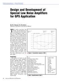
It is possible to use on-chip inductors to increase integration, decrease external component<br />
count, thus reducing the price of the overall LNA. Unfortunately, on-chip inductors have a series<br />
resistance, which reduces their Q to 3-5 at 1GHz. On-chip inductors were not used for the<br />
input-matching network to prevent a noise figure increase, but it is possible to use on-chip<br />
inductors for the load inductance without degradation of performance. A load inductance loss is<br />
already introduced to stability the amplifier at low frequencies. This resistance of the on-chip<br />
inductor can be subtracted from this loss to yield the same performance amplifier. Off-chip<br />
inductors manufactured by Toko, with Q values between 30 and 60 at around 2 GHz, were<br />
assumed for the input matching network. When compared with an on-chip inductor with a Q value<br />
of 3, the input-referred noise power increased by 20%, which would give a large 0.3dB increase<br />
in noise figure.<br />
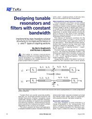
The input-matching network used is a first order high-pass filter. In our final version we used a<br />
series input capacitance of 2.5pF and a shunt inductance of 11nH (Q is assumed to be 50). DC<br />
coupling between the input and the LNA has been achieved by using a capacitance of 100pF.<br />
According to our simulations, this network provides a good compromise between the power and<br />
noise source input impedance.<br />
The output-matching network used is a 5.5nH shunt inductor and a series capacitance of<br />
800fF. The inductor is in series with a 10 ballast resistance and both of them are placed between<br />
the voltage supply and the output node. The capacitance also enables us to get DC coupling<br />
between the amplifier and the output.<br />
Conclusions<br />
A 2.7V 1.9 GHz low noise amplifier with a noise figure of 1.31 dB, transducer power gain of<br />
14.25 dB, an S11 of -14 dB and IIP3 of 7.75dBm has been presented. Unconditional stability at<br />
all frequencies with negligible loss in performance has been guaranteed with carefully placed<br />
resistances in the load matching networks. An automated LNA design procedure has been<br />
developed to optimize and enhance the speed of the designing low noise amplifiers. The design<br />
procedure includes a new method for trading the optimal noise and power source impedances of<br />
the amplifier.<br />
References<br />
[1] Microwave Engineering, 2nd edition, 1998, David M. Pozar, pg. 208.<br />
[2] "Analysis and Design of Monolithic Integrated Mixer," by Keng Fong, U.C. Berkeley Ph. D.<br />
thesis, 1997.<br />
[3] "The implementation of a High Speed Experimental Transceiver Module with an Emphasis on<br />
CDMA Applications," by Arya Reza Behzad, U.C. Berkeley Electronics Research Laboratory<br />
Memorandum No. UCB/ERL M95/40<br />
[4] "RF Circuit Design," by Chris Bowick, 1982, Butterworth Heinemann Publishers