Mathcad - ee217projtodonew2.mcd
Mathcad - ee217projtodonew2.mcd
Mathcad - ee217projtodonew2.mcd

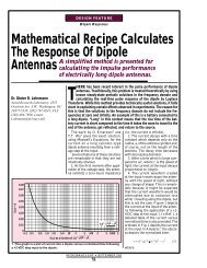
Create successful ePaper yourself
Turn your PDF publications into a flip-book with our unique Google optimized e-Paper software.
∆f: The frequency spacing of the undesired signals from the desired signals. This is used for<br />
distortion calculations.<br />
S11: The maximum desired S11 is determined by the external filter connected to the LNA.<br />
This external filter relies on the low noise amplifier to have a certain impedance to provide given<br />
filtering characteristics.<br />
Gain: The minimum and maxmium desired gain constraints are set by the noise of the<br />
system behind the amplifier.<br />
V DD : The supply voltage is set by the end-of life voltage of three Lithium Ion AA batteries<br />
plus some loss for a voltage regulator. Normally they are 1.5V each, which corresponds to a<br />
normal operating voltage of 4.5V. At end of life they are 1V each, which corresponds to a 3V<br />
supply. The voltage regulator output can vary up to 10%, which gives a minimum supply voltage<br />
of 2.7V.<br />
Temp: The normal operating temperature of the device is a room temperature of 27C plus<br />
some die heating of 15C to due nonideal heat sinking. The actual operating temperature in a<br />
worst case environment may vary between -30C and 105C, but was not added to the design<br />
routine, because of time constraints.<br />
Z bias : The bias impedance is chosen by the practical size limitation of an on-chip inductor to<br />
be used as a bias choke. A 50nH inductor is assumed with a Q of 3 at 1.9 GHz.<br />
K Factor: The desired minimum K factor is somewhat of a guess. In order to simultaneously<br />
conjugate match the input and output ports of the device, the K factor must be greater than one.<br />
If the K factor is set equal to one the real part of the conjugate matching impedance of the source<br />
becomes zero ohms, which is infeasible. For this reason the K factor is set to a value somewhat<br />
larger than one. Although the value was chosen with an educated guess, a real practical value<br />
for K can be calculated by setting a lower limit to the input impedance or an upper limit to the<br />
input matching network, and using it to solve for the K.<br />
NF: The noise figure is determined by the value of the received signal when the cellular<br />
phone is operated at it’s farthest distance from the base station. Here the noise level of the<br />
receiver must be a significant value below the small desired signal.<br />
IP 3 : The third order intercept point is a measure of the low noise amplifiers ability to reject<br />
unwanted signals, such as another cellular phone. When the cellular phone is being used at it’s<br />
greatest distance from base station the phone must be able distinguish the desired signal from<br />
another cellular phone.<br />
∆f 10 MHz Jammer Frequency Spacing<br />
f 1900 MHz ω 2. π . f s j. ω<br />
Frequency of Desired Signal<br />
S 11goaldB 15 dB Input Match Requirement<br />
IP 3goaldBm 10 dBm 3rd Order Intercept Point Requirement<br />
G goaldB 13.5 dB G min 12 dB G max 15 dB Available Power Gain Requirement<br />
Z bias 100 Ω j2 . . π . f 50<br />
. nH Bias Impedance<br />
K val 1.1 Desired In-band Stability Factor<br />
V DD 2.7 V Supply Voltage<br />
Temp 300 K Operating Temperature<br />
N 40 Number of Devices in Parallel<br />
10. mA<br />
Bias Current<br />
I C<br />
The optimizer will find the best value for current and area. The entered values are used for<br />
function testing purposes and graphing.<br />
C/(N+I) Optimization Inputs