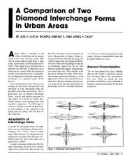
Controller - Institute of Transportation Engineers
Controller - Institute of Transportation Engineers
Controller - Institute of Transportation Engineers

You also want an ePaper? Increase the reach of your titles
YUMPU automatically turns print PDFs into web optimized ePapers that Google loves.
5.4.2.10<br />
A 22-line minimum HAR 2 Harness shall be provided between EX2 Connector and Type<br />
2070-6 Serial COMM Module in the 2070 UNIT. This provides two Modems or EIA-232<br />
Interfaces with the 2070 UNIT and the outside world.<br />
5.4.2.11 Fault and Voltage Monitor Circuitry<br />
NEMA TS1 and TS2 <strong>Controller</strong> FAULT and VOLTAGE MONITOR functions (outputs<br />
to cabinet monitor) shall be provided.<br />
5.4.2.11.1<br />
Two 3-input OR gates shall be provided. The gate 1 output shall be connected to<br />
Connector A, Pin A (FAULT MONITOR) and gate 2 output shall be connected to<br />
Connector A, Pin C. Any FALSE state input shall cause a gate output FALSE (+24VDC)<br />
state.<br />
5.4.2.11.2<br />
The FCU Port 10, Bit 7 output shall normally change its state every 100 ms. A MODULE<br />
Watchdog (WDT) circuit shall monitor the output. No state change for 2 ±0.1 seconds<br />
shall cause the circuit output to generate a FALSE (+24 VDC) output (input to gates 1<br />
and 2). Should the FCU begin changing state, the WDT output shall return to TRUE (0<br />
VDC) state.<br />
5.4.2.11.3<br />
The module shall have a +5 VDC monitoring circuit which monitors the module’s +5<br />
VDC (±0.25). If the voltage exceeds the limits, the circuit output shall generate a FALSE<br />
output (input to gates 1 and 2). Normal operation shall return the output state to TRUE<br />
state.<br />
5.4.2.11.4<br />
The FCU microprocessor output shall be assigned to FAULT Monitor (input to gate 1)<br />
and another output shall be assigned to VOLTAGE Monitor (input to gate 2).<br />
5.4.2.11.5<br />
CPU Port 5 SET OUTPUT COMMAND Message OUTPUTs O78 and O79 shall be<br />
assigned to FAULT (O78) and VOLTAGE (O79). The bit logic state “1” shall be FCU<br />
output FALSE.<br />
5.4.2.11.6<br />
Standard for the ATC – Type 2070 March 29, 2001<br />
91