- Page 1 and 2: PISCES-2ET and Its Application Subs
- Page 3 and 4: Table of Contents Table of Contents
- Page 5 and 6: Table of Contents DOPING . . . . .
- Page 7 and 8: Table of Contents 15 Use of Mixed-M
- Page 9: PART I PISCES-2ET 2D Device Simulat
- Page 12 and 13: Introduction and Acknowledgment Thi
- Page 14 and 15: Introduction and Acknowledgment 4 P
- Page 16 and 17: DUET Carrier Transport Model 2.1 Bo
- Page 18 and 19: DUET Carrier Transport Model genera
- Page 20 and 21: DUET Carrier Transport Model ∂w -
- Page 22 and 23: DUET Carrier Transport Model 2.3 Bo
- Page 24 and 25: Physical Models µ ( N, T L , E ⊥
- Page 26 and 27: Physical Models where α( N ) ( N
- Page 28 and 29: Physical Models 3.1.1.6 “Carrier-
- Page 30 and 31: Physical Models 3.1.2.2 Lombardi’
- Page 32 and 33: Physical Models 1 E ⊥, eff = ε s
- Page 34 and 35: Physical Models SiO 2 interface. To
- Page 36 and 37: Physical Models monotonically in a
- Page 38 and 39: Physical Models 3.3 Recombination a
- Page 40 and 41: Physical Models The third modeling
- Page 42 and 43: Physical Models 32 PISCES-2ET - 2D
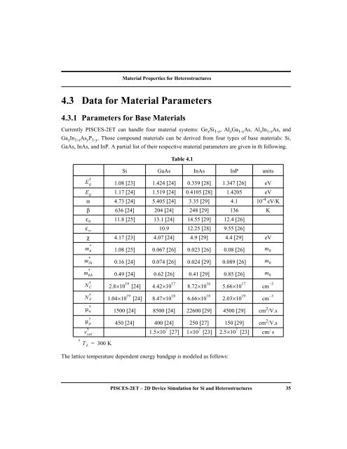
- Page 46 and 47: Material Properties for Heterostruc
- Page 48 and 49: Material Properties for Heterostruc
- Page 50 and 51: Material Properties for Heterostruc
- Page 52 and 53: Material Properties for Heterostruc
- Page 54 and 55: Numerical Techniques p has the dime
- Page 56 and 57: Numerical Techniques Instead of emp
- Page 58 and 59: Numerical Techniques needed during
- Page 60 and 61: Numerical Techniques be applied to
- Page 62 and 63: Numerical Techniques 1 s p, 1 → 2
- Page 64 and 65: Numerical Techniques c equal to 1,
- Page 66 and 67: Numerical Techniques 56 PISCES-2ET
- Page 68 and 69: Simulation Examples It can be clear
- Page 70 and 71: Simulation Examples 10 -1 10 -2 10
- Page 72 and 73: Simulation Examples plot.1d dop log
- Page 74 and 75: Simulation Examples guarantees the
- Page 76 and 77: Simulation Examples elec num=2 ix.l
- Page 78 and 79: Simulation Examples title LED Simul
- Page 80 and 81: Simulation Examples Figure 6.9 Simu
- Page 82 and 83: Simulation Examples $ doping region
- Page 84 and 85: Simulation Examples Figure 6.11 Reg
- Page 86 and 87: Simulation Examples 76 PISCES-2ET -
- Page 88 and 89: Fermi-Dirac Distribution and Hetero
- Page 90 and 91: Fermi-Dirac Distribution and Hetero
- Page 92 and 93: Fermi-Dirac Distribution and Hetero
- Page 94 and 95:
Fermi-Dirac Distribution and Hetero
- Page 96 and 97:
Fermi-Dirac Distribution and Hetero
- Page 98 and 99:
Mathematical Properties of Fermi In
- Page 100 and 101:
Mathematical Properties of Fermi In
- Page 102 and 103:
Formulations in Previous PISCES-II
- Page 104 and 105:
[13] H. Shin, G. M. Yeric, A. F. Ta
- Page 106 and 107:
[41] Z. Yu, R.W. Dutton, and M. Van
- Page 108 and 109:
string, indicates TRUE while a logi
- Page 110 and 111:
Table M.1 Abbreviation for units us
- Page 112 and 113:
CHECK Samemesh A logical flag indic
- Page 114 and 115:
CONTACT COMMAND CONTACT The CONTACT
- Page 116 and 117:
CONTACT MO.disilicide A logical fla
- Page 118 and 119:
CONTACT EXAMPLES CONTACT ALL NEUTRA
- Page 120 and 121:
CONTOUR J.Hole = | J.Displa = | J
- Page 122 and 123:
CONTOUR Flowlines A logical flag fo
- Page 124 and 125:
CONTOUR TEMP.Elec, TEMP.Hole, TEMP.
- Page 126 and 127:
DEEPIMPURITY EXAMPLES DEEPIMP UNIF
- Page 128 and 129:
DOPING DOSe = CHaracter = or COnc
- Page 130 and 131:
DOPING AScii without SUprem3 allows
- Page 132 and 133:
DOPING Lat.char A real number for t
- Page 134 and 135:
DOPING X.Left, X.Right, Y.Top, Y.Bo
- Page 136 and 137:
DOPING COM *** COLLECTOR *** DOP RE
- Page 138 and 139:
ELECTRODE the device structure. If
- Page 140 and 141:
ELIMINATE COMMAND ELIMINATE The ELI
- Page 142 and 143:
END (QUIT) COMMAND END (QUIT) The E
- Page 144 and 145:
EXTRACT bounded region designated b
- Page 146 and 147:
IMPACT COMMAND IMPACT The IMPACT ca
- Page 148 and 149:
INCLUDE COMMAND INCLUDE The INCLUDE
- Page 150 and 151:
INTERFACE Qf Real number for the in
- Page 152 and 153:
LOAD INFile or IN1file, IN2file Cha
- Page 154 and 155:
LOG COMMAND LOG The LOG card allows
- Page 156 and 157:
MATERIAL COMMAND MATERIAL The MATER
- Page 158 and 159:
MATERIAL ETrap Trap level = E t -E
- Page 160 and 161:
MATERIAL Table M.2 material paramet
- Page 162 and 163:
MESH smoothing key: SMooth.key = d
- Page 164 and 165:
MESH OUTFile Specifies the name of
- Page 166 and 167:
MESH MESH GEOM INF=mos.geom POLY.EL
- Page 168 and 169:
METHOD Gemmul iteration) SInglepois
- Page 170 and 171:
METHOD DVlimit Real number paramete
- Page 172 and 173:
METHOD continuity equation is only
- Page 174 and 175:
MOBILITY COMMAND MOBILITY The MOBIL
- Page 176 and 177:
MOBILITY CNPre, CPPre Real number p
- Page 178 and 179:
MOBILITY Qss.conc Real number param
- Page 180 and 181:
MODELS COMMAND MODELS The MODELS ca
- Page 182 and 183:
MODELS ARora A logical flag specify
- Page 184 and 185:
MODELS ENgy.mob) by field-temperatu
- Page 186 and 187:
MODELS IMP.TP A logical flag to ind
- Page 188 and 189:
MODELS TAU.WN, TAU.WP Real number p
- Page 190 and 191:
OPTIONS COMMAND OPTIONS The OPTIONS
- Page 192 and 193:
OPTIONS file will be in a format sp
- Page 194 and 195:
PLOT.1D or TEMP.Hol = | TEMP.Lat =
- Page 196 and 197:
PLOT.1D INFile Character string for
- Page 198 and 199:
PLOT.1D Spline, NSpline The Spline
- Page 200 and 201:
PLOT.1D X.Start, X.End, Y.Start, Y.
- Page 202 and 203:
PLOT.2D COMMAND PLOT.2D The PLOT.2D
- Page 204 and 205:
PLOT.2D L.Elect, L.Deple, L.Junct,
- Page 206 and 207:
PRINT COMMAND PRINT The PRINT card
- Page 208 and 209:
PRINT POints A logical flag to prin
- Page 210 and 211:
REGION COMMAND REGION The REGION ca
- Page 212 and 213:
REGION NItride or SI3n4 A logical f
- Page 214 and 215:
REGION EXAMPLES REGION NUM=1 IX.LO=
- Page 216 and 217:
REGRID COMMAND REGRID The REGRID ca
- Page 218 and 219:
REGRID DOPFile Character string for
- Page 220 and 221:
REGRID always generated to assist f
- Page 222 and 223:
SOLVE COMMAND SOLVE The SOLVE card
- Page 224 and 225:
SOLVE BAnd A logical flag to includ
- Page 226 and 227:
SOLVE MAx.inner Integer parameter f
- Page 228 and 229:
SOLVE TOlerance Real number paramet
- Page 230 and 231:
SOLVE SOLVE V1=0 V2=0 V3=1 VSTEP=.5
- Page 232 and 233:
SPREAD COMMAND SPREAD The SPREAD ca
- Page 234 and 235:
SPREAD Vol.ratio Real number parame
- Page 236 and 237:
SYMBOLIC COMMAND SYMBOLIC The SYMBO
- Page 238 and 239:
SYMBOLIC Min.degree A logical flag
- Page 240 and 241:
TITLE COMMAND TITLE The TITLE card
- Page 242 and 243:
VECTOR J.Conduc, J.Displa, J.Electr
- Page 244 and 245:
X.MESH, Y.MESH Ratio Real number pa
- Page 247 and 248:
Acknowledgment This project was sup
- Page 249 and 250:
SECTION 7 Introduction In Technolog
- Page 251 and 252:
SECTION 9 Trace File The trace spec
- Page 253 and 254:
Trace File which the curve tracing
- Page 255 and 256:
Trace File 9.3.2 Syntax Simulations
- Page 257 and 258:
Trace File none of the solutions is
- Page 259 and 260:
Trace File Tracer run in which volt
- Page 261 and 262:
Input Deck Specifications inputfile
- Page 263 and 264:
Data Format in Output Files with an
- Page 265 and 266:
SECTION 13 Examples In each of the
- Page 267 and 268:
Examples fixed num = 1 type=voltage
- Page 269 and 270:
Examples Collector Current / amps/
- Page 271 and 272:
Examples title mes.pis mesh nx=53 n
- Page 273 and 274:
Examples title mesvg.5.pis option n
- Page 275 and 276:
Examples #Soln #Vctrl Ictrl I2 1 0.
- Page 277:
PART III Mixed-Mode Device/Circuit
- Page 280 and 281:
266 Mixed-Mode Device/Circuit Simul
- Page 282 and 283:
Mixed-Mode Circuit and Device Simul
- Page 284 and 285:
Mixed-Mode Circuit and Device Simul
- Page 286 and 287:
Mixed-Mode Circuit and Device Simul
- Page 288 and 289:
Mixed-Mode Circuit and Device Simul
- Page 290 and 291:
Use of Mixed-Mode Simulation COMMAN
- Page 292 and 293:
Use of Mixed-Mode Simulation Electr
- Page 294 and 295:
Use of Mixed-Mode Simulation For th
- Page 296 and 297:
Use of Mixed-Mode Simulation vmax T
- Page 298 and 299:
Use of Mixed-Mode Simulation curren
- Page 300 and 301:
Use of Mixed-Mode Simulation 15.3 R
- Page 302 and 303:
Use of Mixed-Mode Simulation soluti
- Page 304 and 305:
Use of Mixed-Mode Simulation prl, n
- Page 306 and 307:
Examples V dd (1) * cmos inverter e
- Page 308 and 309:
Examples * S11 x S22 Figure 16.3 S-
- Page 310 and 311:
Examples * supply line Vdd 1 0 5 *
- Page 312 and 313:
Examples Data Lines 5 4 3 2 1 0 C C
- Page 314 and 315:
Examples +5 V Vcc 0.1 µF 10 µF 33
- Page 316 and 317:
Examples 120 100 80 60 I hp1 (mA) 4
- Page 318 and 319:
System Reconfiguration for a Differ
- Page 320 and 321:
System Reconfiguration for a Differ
- Page 322 and 323:
System Reconfiguration for a Differ
- Page 324 and 325:
System Reconfiguration for a Differ
- Page 326 and 327:
System Reconfiguration for a Differ
- Page 328 and 329:
System Reconfiguration for a Differ