
Create successful ePaper yourself
Turn your PDF publications into a flip-book with our unique Google optimized e-Paper software.
SMA<br />
SMA<br />
SMA<br />
SMA<br />
SMA<br />
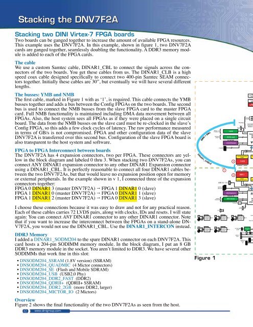
Stacking the DNV7F2A<br />
Stacking two DINI Virtex-7 <strong>FPGA</strong> boards<br />
Two boards can be ganged together to increase the amount of available <strong>FPGA</strong> resources.<br />
This example uses the DNV7F2A. In this example, shown in figure 1, two DNV7F2A<br />
cards are ganged together, seamlessly doubling the functionality. A DDR3 memory module<br />
is added to each of the <strong>FPGA</strong> cards.<br />
<strong>The</strong> cable<br />
We use a custom Samtec cable, DINAR1_CBL to connect the signals across the connectors<br />
of the two boards. You get these cables from us. <strong>The</strong> DINAR1_CLB is a high<br />
speed coax cable designed specifically to connect two 400-pin Samtec SEAM connectors<br />
together. Initially these cables are 30”, but eventually we will have several different<br />
lengths.<br />
<strong>The</strong> busses: YMB and NMB<br />
<strong>The</strong> first cable, marked in Figure 1 with as ‘1’, is required. This cable connects the YMB<br />
busses together and adds a bus between the Config <strong>FPGA</strong>s on the two boards. <strong>The</strong> second<br />
bus is used to connect the NMB busses from the slave <strong>FPGA</strong> card to the master <strong>FPGA</strong><br />
card. Full NMB functionality is maintained including DMA data movement between all<br />
<strong>FPGA</strong>s. Also, the host system sees all <strong>FPGA</strong>s as if they were placed on a single circuit<br />
board. <strong>The</strong> data from the NMB busses on the slave card must be re-clocked in the slave’s<br />
Config <strong>FPGA</strong>, so this adds a few clock cycles of latency. <strong>The</strong> raw performance measured<br />
in terms of GB/s is not compromised. <strong>FPGA</strong> and other configuration data of the slave<br />
DNV7F2A is transferred over this second bus. Configuration of the slave <strong>FPGA</strong> board is<br />
also transparent to the host system and software.<br />
<strong>FPGA</strong> to <strong>FPGA</strong> Interconnect between boards<br />
<strong>The</strong> DNV7F2A has 4 expansion connectors, two per <strong>FPGA</strong>. <strong>The</strong>se connectors are yellow<br />
in the block diagram and labeled 0 thru 3. When stacking two DNV7F2As, you can<br />
connect ANY DINAR1 expansion connector to any other DINAR1 Expansion connector<br />
using a DINAR1_CBL. It is perfectly reasonable to connect all four DINAR1 cables between<br />
the two DNV7F2As, but that would leave no expansion position open for memory<br />
or external peripherals. In the example shown in v 1, I connected three of the expansion<br />
connectors together:<br />
<strong>FPGA</strong> 0 DINAR1 3 (master DNV7F2A) → <strong>FPGA</strong> 1 DINAR1 0 (slave)<br />
<strong>FPGA</strong> 1 DINAR1 0 (master DNV7F2A) → <strong>FPGA</strong> 0 DINAR1 1 (slave)<br />
<strong>FPGA</strong> 1 DINAR1 2 (master DNV7F2A) → <strong>FPGA</strong> 0 DINAR1 3 (slave)<br />
I choose these connections because it was easy to draw and not for any practical reason.<br />
Each of these cables carries 72 LVDS pairs, along with clocks, IDs and resets. I will state<br />
again: You can connect ANY DINAR1 connector to any other DINAR1 connector. Note<br />
that if you want to increase the interconnect between the <strong>FPGA</strong>s on a stand-alone DN-<br />
V7F2A, you would not use the DINAR1_CBL. Use the DINAR1_INTERCON instead.<br />
DDR3 Memory<br />
I added a DINAR1_SODM204 to the spare DINAR1 connector on each DNV7F2A. This<br />
card hosts a 204-pin SODIMM memory module. In the block diagram, I put an 8 GB<br />
DDR3 memory module in the socket. You aren’t limited to DDR3. We have several other<br />
SODIMMs that work fine in this slot:<br />
• DNSODM204_SSRAM (1.8V version) (SSRAM)<br />
• DNSODM204_QUADMIC (4 Mictor connectors)<br />
• DNSODM204_SE (Flash and Mobile SDRAM)<br />
• DNSODM204_USB (USB2.0 Phy)<br />
• DNSODM204_DDR2_FAST (DDR2)<br />
• DNSODM204_QDRII+ (QDRII+ SSRAM)<br />
• DNSODM204_DDR2_2GB (more DDR2, larger)<br />
• DNSODM204_MICTOR_IO (2 Mictors)<br />
Overview<br />
Figure 2 shows the final functionality of the two DNV7F2As as seen from the host.<br />
12<br />
www.dinigroup.com<br />
DINAR1_CABLE<br />
24<br />
MHz<br />
24<br />
MHz<br />
YMB + NMB<br />
114.285 MHz<br />
Frequency<br />
Synthesizer<br />
(Si5326)<br />
114.285 MHz<br />
Frequency<br />
Synthesizer<br />
(Si5326)<br />
G0<br />
G3<br />
40 GbE or<br />
4, 10 GbE<br />
10GbE<br />
Ethernet<br />
24<br />
MHz<br />
24<br />
MHz<br />
Figure 1<br />
10GbE<br />
Ethernet<br />
USB 3.0 / 2.0<br />
SATA II<br />
(device)<br />
JTAG<br />
SATA II<br />
0<br />
1<br />
1<br />
114.285 MHz<br />
Frequency<br />
Synthesizer<br />
(Si5326)<br />
114.285 MHz<br />
Frequency<br />
Synthesizer<br />
(Si5326)<br />
QSFP+<br />
SFP+ Socket<br />
DNSEAM_NS<br />
GTX Expansion<br />
G1<br />
G4<br />
2<br />
4<br />
5<br />
6<br />
GTX Expansion<br />
DNSEAM_NS<br />
SFP+ Socket<br />
24<br />
MHz<br />
1<br />
Config Clk<br />
DINAR1_SODM204<br />
DINAR1_SODM204<br />
10/100/1000<br />
baseT<br />
USB 2.0<br />
(2X)<br />
Stacking<br />
PCIe<br />
(GEN2)<br />
iPASS<br />
4<br />
DINAR1<br />
Expansion Connector<br />
OSC<br />
114.285 MHz<br />
1<br />
8<br />
8<br />
1<br />
1<br />
PCIe<br />
(GEN2)<br />
iPASS<br />
Frequency<br />
Synthesizer<br />
(Si5326)<br />
4<br />
RJ45<br />
RS232<br />
SATA II<br />
(host)<br />
2x<br />
Global<br />
Clocks<br />
72<br />
72<br />
DINAR1<br />
Expansion Connector<br />
DDR 3<br />
DDR 3<br />
72<br />
72<br />
4<br />
G2<br />
3<br />
10/100/1000<br />
Phy<br />
6Mb<br />
FLASH<br />
oot<br />
8Mb<br />
SPI<br />
FLASH<br />
x 64<br />
DR2<br />
5<br />
5<br />
5<br />
DNNMB<br />
onnector<br />
400 pins)<br />
T<br />
T<br />
761]<br />
A<br />
0<br />
r<br />
Ex<br />
FP<br />
7V<br />
7V<br />
[F(F/H<br />
GEN1<br />
Step Clo<br />
RGM<br />
2<br />
R