
You also want an ePaper? Increase the reach of your titles
YUMPU automatically turns print PDFs into web optimized ePapers that Google loves.
DNBFC_S12_PCIe<br />
Expansion<br />
Cards<br />
/<br />
Board to Board<br />
Dataflow<br />
DDR3 - 800<br />
(128M x 16)<br />
DDR3 - 800<br />
(128M x 16)<br />
DDR3 - 800<br />
(128M x 16)<br />
DDR3 - 800<br />
(128M x 16)<br />
DDR3 - 800<br />
(128M x 16)<br />
DDR3 - 800<br />
(128M x 16)<br />
Top<br />
Bottom<br />
QSE<br />
QSE<br />
16<br />
data<br />
16<br />
data<br />
16<br />
data<br />
16<br />
data<br />
16<br />
data<br />
16<br />
data<br />
DDR3 - 800<br />
(128M x 16)<br />
DDR3 - 800<br />
(128M x 16)<br />
data<br />
16<br />
data<br />
16<br />
GTP<br />
GTP<br />
Spartan - 6<br />
LX150T<br />
User <strong>FPGA</strong><br />
Dataflow<br />
Manager<br />
GTP<br />
4 4 4 4<br />
DM<br />
77<br />
77<br />
Spartan - 6<br />
LX150<br />
<strong>FPGA</strong> 0<br />
(FGG484)<br />
64<br />
Spartan - 6<br />
LX150<br />
<strong>FPGA</strong> 11<br />
(FGG484)<br />
77<br />
MB (upper)<br />
MB (lower)<br />
77<br />
Spartan - 6<br />
LX150<br />
<strong>FPGA</strong> 1<br />
(FGG484)<br />
8<br />
8<br />
64<br />
Spartan - 6<br />
LX150<br />
<strong>FPGA</strong> 10<br />
(FGG484)<br />
77<br />
77<br />
Spartan - 6<br />
LX150<br />
<strong>FPGA</strong> 2<br />
(FGG484)<br />
64<br />
Spartan - 6<br />
LX150<br />
<strong>FPGA</strong> 9<br />
(FGG484)<br />
77<br />
77<br />
Spartan - 6<br />
LX150<br />
<strong>FPGA</strong> 3<br />
(FGG484)<br />
64<br />
Spartan - 6<br />
LX150<br />
<strong>FPGA</strong> 8<br />
(FGG484)<br />
77<br />
77<br />
Spartan - 6<br />
LX150<br />
<strong>FPGA</strong> 4<br />
(FGG484)<br />
64<br />
Spartan - 6<br />
LX150<br />
<strong>FPGA</strong> 7<br />
(FGG484)<br />
77<br />
77<br />
Spartan - 6<br />
LX150<br />
<strong>FPGA</strong> 5<br />
(FGG484)<br />
Spartan - 6<br />
LX150<br />
<strong>FPGA</strong> 6<br />
(FGG484)<br />
64 77<br />
32<br />
32<br />
16<br />
data<br />
16<br />
data<br />
16<br />
data<br />
16<br />
data<br />
16<br />
data<br />
16<br />
data<br />
Config<br />
EE<br />
User<br />
EEPROM<br />
PCIe<br />
Bridge<br />
Q<br />
4-lane PCIe (GEN1/GEN2)<br />
DDR3 - 800<br />
(128M x 16)<br />
100MHz Clock<br />
ALL <strong>FPGA</strong>s<br />
MB Clock<br />
DDR3 - 800<br />
(128M x 16)<br />
JTAG<br />
0<br />
DM<br />
1 2<br />
11<br />
10<br />
3<br />
9<br />
4<br />
5<br />
8<br />
6<br />
7<br />
DDR3 - 800<br />
(128M x 16)<br />
Frequency<br />
Synthesizer<br />
31.25 MHz-<br />
350 MHz<br />
DDR3 - 800<br />
(128M x 16)<br />
CLK A<br />
ALL <strong>FPGA</strong>s<br />
DDR3 - 800<br />
(128M x 16)<br />
Battery<br />
Bitstream<br />
Encryption<br />
DDR3 - 800<br />
(128M x 16)<br />
PCIe<br />
Features<br />
• PCI Express (4-lane) <strong>FPGA</strong>-based algorithm acceleration peripheral<br />
- 12 of the largest Xilinx Spartan-6 <strong>FPGA</strong>s: 6SLX150-2<br />
• 12, 128M x 16 (2Gb) DDR3-800 memories (1 per <strong>FPGA</strong>)<br />
- 1 Xilinx Spartan-6 <strong>FPGA</strong>s: 6SLX150T-2<br />
• 2, 128M x 16 (2Gb) DDR3-800 memories<br />
• Fixed 4-lane PCIe interface and controller<br />
- PCIe GEN1/GEN2<br />
- Full mastering DMA<br />
• 2 transmit (host memory -> card)<br />
• 2 receive (card -> host memory)<br />
• Xilinx <strong>FPGA</strong> Spartan-6 LX150-2 – 12 total<br />
- 184,464 flip-flops per <strong>FPGA</strong><br />
• 92K flips-flops with 6-input LUT<br />
- 180, 18x18 multipliers + 48-bit accumulator per <strong>FPGA</strong><br />
- 268, 18 Kbit block RAM (603 Kbytes) per <strong>FPGA</strong><br />
• Fully dual-ported<br />
• Each block RAM configurable as:<br />
- 16K×1, 8K×2, 4K×4, 2K×8/9, 1K×16/18, or 512 x 32/36<br />
- Options for LX150-1L (lower power) or LX150-3 (higher frequency)<br />
• Also LX150T-3,-4<br />
- Options for LX100, LX75, LX45, LX25 (lower cost)<br />
• <strong>FPGA</strong> to <strong>FPGA</strong> interconnect single-ended<br />
- Source synchronous <strong>FPGA</strong> -> <strong>FPGA</strong> frequency: 150MHz<br />
• 300 Mb/s per pin when using DDR<br />
• Main Bus (MB) connects all Spartan-6 <strong>FPGA</strong>s (8 signals)<br />
- 90MHz<br />
• 128Mb x 16 fixed external DDR3 memory dedicated to each field <strong>FPGA</strong> (12 total)<br />
• 2 – 128Mb x 16 fixed external DDR3 memories dedicated to USER<br />
Dataflow Manager <strong>FPGA</strong><br />
- DDR3-800 is stuffed. VCCINT is set to ‘Extended Performance’ operating range:<br />
• With LX150-2, LX150T-2: 667 Mbps (333.5 MHz)<br />
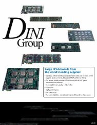
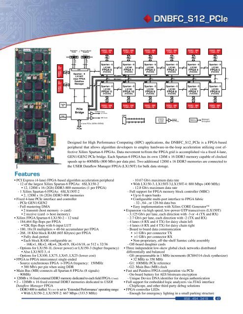
Designed for High Performance Computing (HPC) applications, the DNBFC_S12_PCIe is a <strong>FPGA</strong>-based<br />
peripheral that allows algorithm developers to employ hardware-in-the-loop acceleration utilizing cost effective<br />
Xilinx Spartan-6 <strong>FPGA</strong>s. Data movement to/from the <strong>FPGA</strong> grid is accomplished via a fixed 4-lane,<br />
GEN1/GEN2 PCIe bridge. Each Spartan-6 <strong>FPGA</strong> has its own 128M x 16 DDR3 memory capable of clocked<br />
speeds up to 400MHz (800 Mb/s per data pin). Two additional 128M x 16 DDR3 memories are connected to<br />
the USER Dataflow Manager <strong>FPGA</strong> (LX150T) for bulk data storage.<br />
- 10.67 Gb/s maximum data rate<br />
• With LX150-3, LX150T-3,LX150T-4: 800 Mbps (400 MHz)<br />
- 12.8 Gb/s maximum data rate<br />
- Full support for <strong>FPGA</strong> memory block controller (MBC)<br />
• Up to 8 open banks<br />
• Configurable multi-port interface to <strong>FPGA</strong> fabric<br />
- 32-, 64-, or 128-bit data bus<br />
• Easy implementation with Xilinx CORE Generator<br />
• Expansion via high speed, low-power GTP transceivers (LX150T)<br />
- 3.125 Gb/s per lane, each direction with -3 or -4 (TX and RX)<br />
- 2.7 Gb/s per lane, each direction with -2 (TX and RX)<br />
- 4 lanes (4 RX and 4 TX) for daisy chain left<br />
- 4 lanes (4 RX and 4 TX) for daisy chain right<br />
- Board to board data communication<br />
• >1 GB/s per connector TX<br />
• >1 GB/s per connector RX<br />
• Non-proprietary, off-the-shelf Samtec cable assembly<br />
- Off-board daughter cards<br />
• Three independent low-skew global clock networks distributed<br />
differentially and balanced<br />
- G0: programmable in 1 MHz increments (ICS84314 clock synthesizer)<br />
• 32 MHz to 350 MHz<br />
- G1: 100MHz PCIe reference<br />
- G2: Main Bus (MB) clock<br />
• Fast and Painless <strong>FPGA</strong> configuration via PCIe<br />
- On-board battery for AES bitstream encryption<br />
- Unique Device DNA identifier for design authentication<br />
• Full support for embedded logic analyzers via JTAG interface<br />
- ChipScope, and other third-party debug solutions<br />
• <strong>FPGA</strong>-controller LEDs<br />
- Enough for emergency lighting in a small parking structure<br />
858 . 454 . 3419 45