
Create successful ePaper yourself
Turn your PDF publications into a flip-book with our unique Google optimized e-Paper software.
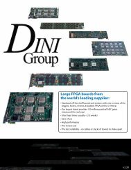
two Virtex-7 <strong>FPGA</strong>s | 7V2000T-1 | 28 million ASIC gates | stackable<br />
Features<br />
• Hosted via<br />
- 4-lane GEN2 PCIe via iPASS cable<br />
- USB2.0<br />
- 10/100/1000BASE-T Ethernet<br />
- Stand alone<br />
• Dual Xilinx Virtex-7 <strong>FPGA</strong>:<br />
- 7V2000T-2,-1 (fastest to slowest)<br />
- 7VX690T-3,-2,-1<br />
• 28+ million ASIC gates (ASIC measure) when<br />
stuffed with two 7V2000T<br />
• GTP low-powered transceivers (assumes -2 speed<br />
grade or faster for 10GbE):<br />
- <strong>FPGA</strong> 0:<br />
• 2 SFP+ sockets<br />
• 4 channels SATA II (device)<br />
• USB3.0<br />
• 2 channels using SMA connectors<br />
• 4-lane PCIe GEN1/GEN2 prototyping via<br />
iPASS cable<br />
• Dual SEARAY GTP Expansion headers,<br />
8-lanes each.<br />
• PCIe,CX4,4 SFP+ sockets or custom<br />
- <strong>FPGA</strong> 1:<br />
• QSFP+ socket<br />
• 4 lanes 10GbE or single lane 40 GbE Ethernet<br />
• 1 SFP+ socket<br />
• 2 channels SATA II (device)<br />
• 4-lane PCIe GEN1/GEN2 prototyping via<br />
iPASS cable<br />
• Dual SEARAY GTP Expansion headers,<br />
8-lanes each<br />
• PCIe,CX4,4 SFP+ sockets, SMA or custom<br />
- Marvel MV78200 Discovery Innovation Dual CPU<br />
• 1 GHz clock<br />
• Dual USB2.0 ports (Type B connector)<br />
• Dual Serial-ATA II connectors for 2 external<br />
hard drives (SATA II)<br />
• Gigabit Ethernet interface<br />
• 10/100/1000 GbE (RJ45 connector)<br />
• Sheeva CPU Core (ARM v5TE compliant)<br />
• Out-of-order execution<br />
• Single and double-precision IEEE compliant<br />
floating point<br />
• DSP instructions boosts performance for signal<br />
processing applications<br />
• MMU to support virtual memory features<br />
• Dual Cache: 32 KB for data and instruction,<br />
parity protected<br />
• L2 cache: 512 KB unified L2 cache per CPU<br />
(total of 1MB), ECC protected.<br />
• 1 GB external DDR2 SDRAM<br />
• Organized in a 128M x 64 configuration<br />
• 400 MHz (800 MHz data rate with DDR)<br />
• RS232 port for terminal-style observation<br />
• After configuration, both CPUs dedicated entirely<br />
to user application<br />
• Linux operating system<br />
• Source and examples provided via GPL license<br />
(no charge)<br />
• ~15 seconds to CPU boot<br />
- Five independent low-skew global clock networks<br />
• G0, G1, G2, G3, G4<br />
• Five, high-resolution, user-programmable syn<br />
thesizers for G0, G1, G2, G3 and G4<br />
• Silicon Labs Si5326: 2kHz to 945 MHz<br />
• User configurable via Marvell uP RS232, USB,<br />
PCIe, or Ethernet<br />
• Global clocks networks distributed differen<br />
tially and balanced<br />
- Flexible customization via 2 daughter cards positions<br />
per <strong>FPGA</strong><br />
• DINAR1 expansion connector<br />
• Connector is non-proprietary, readily available,<br />
and cheap<br />
• 72 LVDS pairs + clocks (or 150 single-ended)<br />
• 700 MHz on all signals with source synchronous<br />
LVDS<br />
• Signal voltage set by daughter card (+1.2V to +1.8V)<br />
• Reset<br />
• Supplied power rails (fused):<br />
• +12V (24W max)<br />
• +3.3V (10W max)<br />
• Pin multiplexing to/from daughter cards using<br />
LVDS (up to 10x)<br />
• Support FMC, logic analyzer, memory expansion<br />
- Fast and Painless <strong>FPGA</strong> configuration<br />
• USB, cabled PCIe, Ethernet, JTAG<br />
• Stand-alone configuration with USB stick<br />
• Configuration Error reporting<br />
• Accelerated configuration readback for advanced<br />
debug<br />
- RS232 port for embedded <strong>FPGA</strong>-based SOC µP debug<br />
• Accessible from all <strong>FPGA</strong>s via separate 2-signal bus<br />
- Full support for embedded logic analyzers via<br />
JTAG interface<br />
• ChipScope, Tektronix Veridae<br />
- Status <strong>FPGA</strong>-controlled LEDs<br />
• Enough multicolored LEDs to illuminate a<br />
medium sized dungeon<br />
858 . 454 . 3419 9