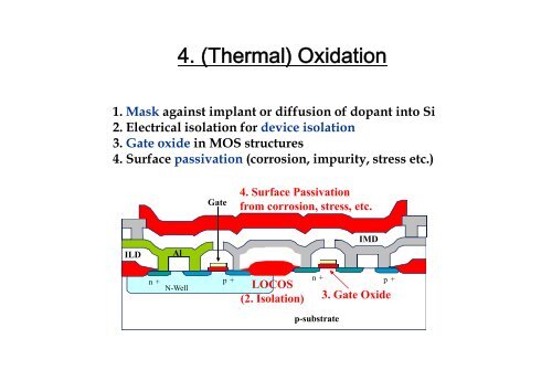
4. (Thermal) Oxidation
4. (Thermal) Oxidation
4. (Thermal) Oxidation
- No tags were found...

You also want an ePaper? Increase the reach of your titles
YUMPU automatically turns print PDFs into web optimized ePapers that Google loves.
<strong>4.</strong> (<strong>Thermal</strong>) <strong>Oxidation</strong><br />
1. Mask against implant or diffusion of dopant into Si<br />
2. Electrical isolation for device isolation<br />
3. Gate oxide in MOS structures<br />
<strong>4.</strong> Surface passivation (corrosion, impurity, stress etc.)<br />
Gate<br />
<strong>4.</strong> Surface Passivation<br />
from corrosion, stress, etc.<br />
ILD<br />
Al<br />
IMD<br />
n +<br />
n-well<br />
N-Well<br />
p + n +<br />
p +<br />
LOCOS<br />
(2. Isolation)<br />
p-substrate<br />
3. Gate Oxide
Applications of Oxide<br />
5. Diffusion Source<br />
6. Dielectric Materials for Capacitor in DRAM<br />
PSG on poly-Si → phosphorous drive-in<br />
PSG<br />
N-Well<br />
n-well<br />
poly-Si for Gate<br />
p-substrate
Prof. Nathan Cheung, U.C. Berkeley<br />
Properties of <strong>Thermal</strong> SiO 2
Prof. Nathan Cheung, U.C. Berkeley
Techniques for Oxide Formation<br />
• RT ~ 200 o C<br />
Ø wet anodization, sputtering<br />
• 250 ~ 600 o C<br />
Ø CVD (SiH 4 + O 2 → SiO 2 + 2H 2 )<br />
• 600 ~ 900 o C<br />
Ø CVD (pyrolysis of Si(OC 2 H 5 ) 4 , SiH 4 , SiCl 4 )<br />
• 900 ~ 1200 o C<br />
Ø THERMAL OXIDATION
<strong>Thermal</strong> <strong>Oxidation</strong> Process<br />
1. <strong>Thermal</strong> oxidation of silicon is achieved by heating the wafer to a high<br />
temperature, typically 800 to 1200 o C, in an atmosphere containing either<br />
pure oxygen or water vapor.<br />
- Dry <strong>Oxidation</strong> : Si(s) + O 2 (g) → SiO 2 (s)<br />
- Wet <strong>Oxidation</strong> : Si(s) + 2H 2 O(v) → SiO 2 (s) + H 2 (g)<br />
- Wet oxidation is used to grow thick oxides, and widely used for an impurity mask.<br />
- Dry oxidation occurs slowly but results in a higher-density oxide than wet oxidation.<br />
è Higher density results in a higher breakdown voltage (5-10 MV/cm)<br />
è Thin gate oxide (
How does oxidation occur<br />
1 st step: At high temperatures, both water vapor and oxygen move (diffuse)<br />
easily through SiO 2 .<br />
2 nd step: Oxygen arriving at the Si surface can combine with Si.<br />
3 rd step: Chemical reaction occurs at the Si surface to form SiO 2 .<br />
• Si is consumed as the oxide grows, and the resulting oxide expands<br />
during growth (Fig. 3.2).<br />
• The final oxide layer is approximately 54% above the original surface<br />
of the silicon and 46% below it.
2. Modeling <strong>Oxidation</strong><br />
1. <strong>Oxidation</strong> occurs at the Si-SiO 2 interface.<br />
2. As the oxide grows, oxygen must pass through more and more oxide.<br />
3. <strong>Oxidation</strong> rate decreases as time goes on.<br />
F 1 F 2 F 3<br />
F 1 = gas phase<br />
F 2 = through oxide<br />
F 3 = reaction flux<br />
Steady State Requires:<br />
F 1 = F 2 = F 3<br />
Figure 3.3<br />
Model for thermal oxidation of silicon. X 0 is the thickness of the silicon dioxide layer at any time t. J<br />
is the constant flux of oxygen diffusing through the layer, and N 0 and N i represent the oxygen<br />
concentration at the oxide surface and silicon dioxide-silicon interface, respectively. Note that the<br />
oxide growth occurs at the silicon interface.
1. Fick’s first law of diffusion : The particle flow per unit area, J (called<br />
particle flux), is directly proportional to concentration gradient of the<br />
particle.<br />
( x,<br />
t) ( N N )<br />
N<br />
i<br />
-<br />
J = F2<br />
= -D<br />
× = -D<br />
x<br />
X<br />
D : diffusion coefficient, N : particle concentration<br />
(-) : particles tend to move from a region of high concentration to<br />
a region of low concentration<br />
X 0 : thickness of the oxide at a given time<br />
N 0 , N i : concentration of the oxidizing species in the oxide at the<br />
oxide surface and SiO 2 -Si interface.<br />
0<br />
0<br />
J = F = k s<br />
× N<br />
3 i<br />
é<br />
ê<br />
ë<br />
number of particles<br />
2<br />
cm ×sec<br />
2. The oxidation rate at the SiO 2 -Si interface is proportional to the<br />
concentration of the oxidizing species.<br />
The flux at the interface:<br />
(3.5)<br />
k s : rate constant for the reaction at the SiO 2 -Si interface.<br />
ù<br />
ú<br />
û<br />
F 1 F 2 F 3
Eliminating N i using F 2 and F 3 ;<br />
\<br />
J<br />
=<br />
æ<br />
ç X<br />
è<br />
D × N<br />
0<br />
+<br />
0<br />
D ö<br />
÷<br />
k s ø<br />
(3.6)<br />
3. The rate of change of thickness of the oxide layer with time is given by the<br />
oxidizing flux divided by the number of molecules M of the oxidizing<br />
species that are incorporated into a unit volume of the resulting oxide:<br />
t<br />
dX<br />
dt<br />
o<br />
=<br />
J<br />
M<br />
=<br />
æ D × N0<br />
ö<br />
ç ÷<br />
è M ø<br />
æ D ö<br />
ç X<br />
0<br />
+<br />
÷<br />
è ks<br />
ø<br />
(3.7)<br />
This differential equation is easily solved by using separation of variables<br />
method with the boundary condition X 0 (t = 0) = X i , which yields<br />
=<br />
X<br />
B<br />
2<br />
o<br />
+<br />
æ<br />
ç<br />
è<br />
X<br />
B<br />
A<br />
o<br />
ö<br />
÷<br />
ø<br />
-t<br />
(3.8)<br />
M :<br />
A =<br />
2D<br />
k s<br />
number of molecules of oxidizing<br />
species in a unit volume of oxide<br />
2DN<br />
M<br />
0<br />
B =<br />
t =<br />
X<br />
B<br />
2<br />
i<br />
X<br />
i<br />
+<br />
æ B ö<br />
ç ÷<br />
è A ø
Solving eq. (3.8) for X 0 (t) yields:<br />
1 1<br />
é<br />
êì<br />
4×<br />
B ü<br />
\ t<br />
2<br />
X ( ) 1 ( ) 1 (3.9)<br />
2<br />
2<br />
ú ú o<br />
t = A í + t + ý -<br />
êî<br />
A þ<br />
ë<br />
û<br />
2<br />
A<br />
t + ><br />
4×<br />
B<br />
4<br />
æ B ö<br />
X o<br />
( t) = ç ÷× ( t +t )<br />
t = B × t<br />
Short Times: ( t )<br />
Long Times: ( t + t ) , t >> t<br />
è<br />
A ø<br />
X o<br />
ù<br />
2<br />
A<br />
× B<br />
( ) ( +t )<br />
•<strong>Oxidation</strong> growth is proportional to time.<br />
•The ratio B/A is called the linear<br />
(growth) rate constant.<br />
•In this region, growth rate is limited by<br />
the reaction at the Si interface.<br />
•<strong>Oxidation</strong> growth is proportional to the<br />
square root of time.<br />
•B is called the parabolic rate constant.<br />
•In this region, the oxidation rate is<br />
diffusion limited.
<strong>Oxidation</strong> Rate (summary)<br />
• Oxide thickness after an oxidizing time t is<br />
A æ t + t ö<br />
x ç<br />
÷<br />
0<br />
= 1+<br />
-1<br />
2<br />
2<br />
è A / 4B<br />
ø<br />
I. For short time (t + t ≪ A 2 /4B)<br />
x 0 = B/A (t + t) : Linear Growth Law<br />
linear rate constant B/A<br />
B/A = C * /N : independent of D<br />
II. For long time (t + t ≫ A 2 /4B)<br />
x 02 = B(t + t) : Parabolic Growth Law<br />
parabolic rate constant B<br />
B = 2DC * /N<br />
→ proportional to D<br />
(diffusion controlled)<br />
At initial stage of oxide growth, when surface reaction is the rate-limiting factor, the oxide<br />
thickness varies linearly with time. As the oxide layer becomes thicker, the oxidant must<br />
diffuse through the oxide layer to react at the Si-SiO 2 interface, and the reaction becomes<br />
diffusion limited. The oxide growth then becomes proportional to the square root of the<br />
oxidizing time, which results in a parabolic growth rate.
*******************************************************************************<br />
참고자료: Solution of differential equation dX 0<br />
/dt = J/M = (DN 0<br />
/M)/(X 0<br />
+ D/k s<br />
)<br />
*******************************************************************************<br />
- Si 표면에서 산화되는 속도는 표면에 존재하는 산소전자의 밀도에 비례 또한 산화가<br />
빨리 될수록 (산소가 빨리 소요될수록) flux도 증가<br />
- 두식으로부터<br />
.<br />
- 산화막 두께의 시간에 따른 변화는
- 변수 분리법에 의해 다음을 얻고,<br />
.<br />
- 양변을 각 변수에 관해 적분하면 다음을 얻는다.<br />
- 경계조건: t = 0에서 X o<br />
= X i<br />
이므로,<br />
∴ 원래의 식은 다음과 같이 된다.
- X o<br />
에 관한 이차 방정식의 근의 공식을 이용하면 다음을 얻는다.<br />
- 위의 최종 식을 oxide 두께의 계산에 사용<br />
경계조건: X o<br />
(t = 0) = X i<br />
: initial oxide thickness (native oxide 혹은 열산화 공정 이전의<br />
oxide 두께)
*******************************************************************************
3. Factors which affect oxidation rate<br />
- Temperature:<br />
is strongly proportional to the temperature during the oxidation process.<br />
- Oxidant species (wet and dry oxidation):<br />
Water vapor has a much higher solubility than O 2<br />
in SiO 2<br />
, which<br />
accounts for much higher oxide growth rate in a wet atmosphere. Slower<br />
growth results in a denser, higher-quality oxide and is usually used for MOS<br />
gate oxides.<br />
- Pressure:<br />
is proportional to the partial pressure of the oxidizing species, so<br />
pressure can be used to control oxide growth rate. High-pressure is being<br />
used to increase oxidation rates at low temperature (Fig. 3.8).<br />
- Crystal orientation:<br />
changes the number of Si bonds available at the Si surface, which<br />
influences the oxide growth rate and quality of the Si-SiO 2 interface.<br />
- Impurity doping:<br />
Heavy doping of Si changes its oxidation characteristics: i.e.,<br />
Phosphorus doping increases the linear rate constant without altering<br />
parabolic rate constant. Boron doping increases the parabolic constant but has<br />
little effect on the linear rate constant.<br />
(100)<br />
(111)<br />
(011)<br />
- Ambient gases:
7. Oxide Quality: Interface and Charges<br />
Oxide<br />
trapped<br />
charge<br />
Mobile ionic charge<br />
K + Na +<br />
+<br />
+<br />
- -<br />
+ + + +<br />
Fixed oxide charge<br />
Interface trapped charge<br />
SiO 2<br />
SiO x<br />
Si<br />
• Interfacial trapped charge:<br />
located at a SiO2-Si interface,<br />
-depends on chemical composition of interface,<br />
crystal orientation.<br />
-typical density ~10 10 /cm 2 for <br />
• Fixed oxide charge:<br />
located in the oxide within 10 -35 Å of interface<br />
-positive, depends on oxidation annealing<br />
conditions, and silicon orientation<br />
-typical density ~ 5x10 10 /cm 2 for <br />
• Oxide trapped charge:<br />
-distributed inside the oxide layer due to x-ray or<br />
high-energy ‘e’ bombardment, cured by low-temp.<br />
annealing<br />
• Mobile Ionic Charge (Q m )<br />
Ø due to contamination from ionized alkali metal atoms (Na + , Ka + )<br />
Ø Drifts from gate/SiO 2 interface to Si/SiO 2 interface under positive gate field<br />
Ø Changes threshold voltage V T in the device
8. Selective <strong>Oxidation</strong><br />
8.1 Local oxidation of silicon (LOCOS)<br />
Fig 3.12 (a)<br />
1 A thin layer of silicon dioxide is grown on the<br />
wafer to protect the silicon surface.<br />
2 A layer of silicon nitride is deposited over the<br />
surface and patterned using photolithography.<br />
3 The wafer goes through a thermal oxidation<br />
step.<br />
4 Some oxide growth occurs under the edges of<br />
the nitride and causes the nitride to bend up at<br />
the edges of the masked area.<br />
This process results in the so-called semirecessed<br />
oxide structure.<br />
Fig. 3.12 (b)<br />
1 A fully recessed oxide can be<br />
formed by etching the silicon<br />
prior to oxidation.<br />
2 This process can yield a very<br />
planer surface after the removal<br />
of the nitride mask.<br />
è subsequent processing reduces<br />
the advantage of this process<br />
over the semi-recessed version.
8.1.1 Deep Trench Isolation<br />
To solve the problem of LOCOS, both the deep and shallow trench techniques<br />
were developed.<br />
Figure 3.13 (a) Deep trench isolation.<br />
- Figure 3.13(a) depicts formation of deep trenches filled<br />
with poly-silicon in combination with a LOCOS field<br />
oxidation.<br />
- A thin oxide pad is grown on Si followed by deposition<br />
of a Si 3 N 4 layer.<br />
- Lithography is used to define openings in the nitride<br />
where trenches will be formed.<br />
- The trenches are etched using reactive-ion etching and<br />
can be deep with high aspect ratios.<br />
- The surface of the trench is passivated with a thin layer<br />
of thermally grown oxide, and then trench is refilled with<br />
deposited poly-silicon.<br />
- The final structure is produced by etching back any<br />
excess poly-silicon, using a lithography step to remove the<br />
nitride layer where oxidation is desired, and growing the<br />
semi-recessed oxide layer.<br />
- The poly-silicon may be doped, and similar structures<br />
are used to form trench capacitors for use as storage<br />
elements .<br />
- The trenches may be as much as 5~10um in depth.
8.1.2 Shallow Trench Isolation<br />
Shallow trench isolation is used to provide isolation between transistors in<br />
MOS & bipolar technology with feature sizes below 0.5um.<br />
- Figure 3.13(b) depicts one possible process flow for forming shallow trenches.<br />
- A shallow trench with tapered sidewalls is etched in the Si following patterning of the nitride layer.<br />
- The pad oxide may be etched away slightly to round the corners of the final structure.<br />
- A thin oxide layer is grown as a liner on the trench walls, and the trench is then filled with an oxide<br />
deposited using decomposition of TEOS or via a high-density plasma deposition.<br />
- A process called chemical mechanical polishing (CMP) is used to remove the excess oxide and create a<br />
highly planar surface.<br />
- Finally, the nitride may be removed, leaving the shallow trench isolation between two Si regions.
8.2 Chemical Mechanical Polishing (CMP)<br />
CMP is a technique to planarize the surface of the sample, and now widely used in both<br />
bipolar & MOS processors to achieve the highly planar topologies required in deep<br />
submicron lithography.<br />
- The wafer is mounted on a rotating pattern.<br />
- A liquid slurry is continuously dispensed onto the surface of the<br />
polishing pad.<br />
- A combination of the vertical force between the wafer and the<br />
abrasive pad as well as the chemical action of the slurry is used to<br />
polish the surface to a highly planar state.<br />
- In the case of formation of the shallow trenches, the nitride layer<br />
serves as a polishing stop. Polishing terminates when the nitride<br />
layer is fully exposed.<br />
Figure 3.15<br />
Chemical mechanical polishing technique<br />
Schematic drawing of a CMP polisher.
9. Oxide Thickness Characterization<br />
H.W<br />
One of the simplest methods for determining the thickness of an oxide:<br />
To compare the color of the wafer with the reference color chart in Table 3.2
When a wafer is illuminated with white light perpendicular to the<br />
surface, the light penetrates the oxide film and is reflected by the<br />
underlying silicon wafer.<br />
The color of the wafer correspond to the enhanced wavelength.<br />
Constructive interference occurs when the path length in the oxide<br />
(2X 0 ) is equal to an integer multiple of one wavelength of light in the<br />
oxide.<br />
2X 0<br />
= kλ / n<br />
k : any integer greater than zero<br />
n : refractive index of the oxide (n = 1.46 for SiO 2<br />
).
Accurate thickness measurement methods:<br />
1) Ellipsometer:<br />
- This instrument is often used to make an accurate reference color chart.<br />
- Polarized monochromatic light is used to illuminate the wafer at an angle to<br />
the surface.<br />
- Light is reflected from both the oxide and silicon surfaces.<br />
- The differences in polarization are measured and the oxide thickness can be<br />
calculated.<br />
2) A mechanical surface profiler can also be used to measure film thickness.<br />
- The oxide is partially etched from the surface of a test wafer to expose a step<br />
between the wafer and oxide surface.<br />
- A stylus is mechanically scanned over the surface of the wafer, and thickness<br />
variations are recorded on a strip-chart recorder. Measurable film thickness<br />
is between 0.01μm and 5μm.<br />
3) A light-interference effects in microscopy can also be used to measure film<br />
thickness accurately.
11. Summary<br />
1. Silicon dioxide provides a high-quality insulating barrier on the surface of silicon wafer.<br />
- This layer can serve as a barrier layer during subsequent impurity diffusion process steps.<br />
2. Thicker layers of silicon dioxide are conveniently grown in high-temperature oxidation<br />
furnaces using wet and dry oxygen.<br />
- <strong>Oxidation</strong> occurs much more rapidly in wet oxygen than in dry oxygen.<br />
- The dry-oxygen environment produces a higher quality oxide and is usually used for the growth<br />
of MOS gate oxides.<br />
- As the oxide becomes thicker, grow rate slows and becomes proportional to the square root of<br />
time.<br />
- These two growth regions are characterized by the linear and parabolic growth-rate constants.<br />
3. Oxide cleanness is extremely important for MOS processes, and great care<br />
is exercised to prevent sodium contamination of the oxide.<br />
- The addition of chlorine during oxidation improves oxide quality.<br />
- <strong>Oxidation</strong> alters the impurity distribution at the surface of the silicon wafer. Boron tends to be<br />
depleted from the silicon surface, whereas phosphorous tends to pile up at the silicon surface.<br />
<strong>4.</strong> <strong>Oxidation</strong> thickness can be accurately measured using ellipsometers,<br />
interference microscopes, and mechanical surface profilers or can be estimated from the<br />
apparent color of the oxide under vertical illumination with white light.
참고자료
<strong>Oxidation</strong> Rate: Temperature & Oxidant<br />
Parabolic B = C 1 exp(-E 1 /kT)<br />
Linear B/A = C 2 exp(-E 2 /kT)<br />
Dry O 2<br />
Wet H 2 O<br />
(640 Torr)<br />
C 1 = 7.72 x 10 2 mm 2 /h<br />
C 2 = 3.71 x 10 6 mm 2 /h<br />
C 1 = 3.86 x 10 2 mm 2 /h<br />
C 2 = 0.97 x 10 8 mm 8 /h<br />
E 1 = 1.23 eV<br />
E 2 = 2.00 eV<br />
E 1 = 0.78 eV<br />
E 2 = 1.96 eV<br />
- The rate-constant data follow straight line when plotted on a semilogarithmic scale vs. reciprocal T<br />
- This type of behavior is referred to as an Arrhenius relationship. D = D 0 exp(-E A /kT ) (3.12)<br />
The rate depends on the surface<br />
bond structure of Si atoms,<br />
à orientation dependence<br />
Independent of crystal<br />
orientation<br />
Temperature dependence of both linear- and parabolic-rate constant
<strong>Oxidation</strong> Rate: Pressure<br />
High pressure increases the oxide growth rate,<br />
by increasing the linear and parabolic rate constants.<br />
( The increase in the rate constants arises from the increased N o .)<br />
B<br />
A<br />
B<br />
kSC0<br />
=<br />
N<br />
DC<br />
=<br />
N<br />
kS<br />
*<br />
@ C<br />
N<br />
2D<br />
@ C<br />
N<br />
2<br />
0<br />
*<br />
kS<br />
= K<br />
H<br />
PG<br />
N<br />
2D<br />
= K<br />
H<br />
P<br />
N<br />
Trade off: DP = 1 atm Û DT = 30 o C<br />
Ø Low temperature oxidation can be<br />
achieved under high pressure for<br />
the same oxidation rate.<br />
G<br />
Method<br />
1. Pressurizing water-pumping<br />
2. Producing water by pyrogenic system
<strong>Oxidation</strong> Rate: Crystal Orientation<br />
(111)<br />
(011)<br />
(100)<br />
• The parabolic rate depends on the D of oxidants through SiO 2 .<br />
• On the other hand, the linear rate constant B/A depending on the reaction k S<br />
at SiO 2 /Si interface is strongly related to the crystallographic orientation of Si.<br />
• The growth rate ratio (v 111 /v 100 ) decreases at high temperatures and at long time<br />
since the parabolic rate constant is predominant. (diffusion-limited)<br />
Ø CO changes the # of Si bonds available at the surface<br />
(100) silicon: the smallest number of unsatisfied Si bonds at the Si-SiO2<br />
interface, and the choice of the (100) orientation yields the lowest number of<br />
interface traps, leading to lowest oxidation rate.
<strong>Oxidation</strong> of Poly-Si
<strong>Oxidation</strong> Rate: Doping<br />
• Heavy doping of silicon also changes its oxidation characteristics.<br />
(i.e., Group III and V dopants enhance the oxidation rate when heavily doped.)<br />
• Depending on the impurity redistributions, oxidation rate depends on<br />
Ø the C B at SiO 2 for diffusion controlled oxidation (B dominates).<br />
Ø the C B at Si surface for reaction controlled oxidation (B/A dominates).<br />
Boron segregated in SiO 2<br />
weakens the SiO 2 bond structures.<br />
ØRapid diffusion of O 2 and H 2 O<br />
Ø(B dominates the process)<br />
Phosphorus piles up at Si surface.<br />
Ø Enhanced oxidation rate in the<br />
reaction controlled regime<br />
(B/A dominates the process)
<strong>Oxidation</strong> Rate: Additional Gases<br />
• Halogenic <strong>Oxidation</strong>:<br />
The presence of chlorine mixed with O 2 gas during dry oxidation<br />
1. Enhances the oxidation rate.<br />
2. Improves device characteristics.<br />
Chlorine-containing gases: Cl 2 , HCl, TCE, TCA