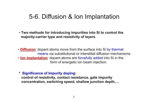
5-6. Diffusion & Ion Implantation
5-6. Diffusion & Ion Implantation
5-6. Diffusion & Ion Implantation

You also want an ePaper? Increase the reach of your titles
YUMPU automatically turns print PDFs into web optimized ePapers that Google loves.
5-<strong>6.</strong> <strong>Diffusion</strong> & <strong>Ion</strong> <strong>Implantation</strong><br />
• Two methods for introducing impurities into Si to control the<br />
majority-carrier type and resistivity of layers<br />
• <strong>Diffusion</strong>: dopant atoms move from the surface into Si by thermal<br />
means via substitutional or interstitial diffusion mechanisms.<br />
• <strong>Ion</strong> implantation: dopant atoms are forcefully added into Si in the<br />
form of energetic ion beam injection.<br />
* Significance of Impurity doping:<br />
control of resistivity, contact resistance, gate impurity<br />
concentration, switching speed, shallow junction depth,…<br />
1
Comparison I<br />
2
Comparison II – Doping Profiles<br />
Figure <strong>6.</strong>1 (p. 105)<br />
Comparison of (a)<br />
diffusion and (b) ionimplantation<br />
techniques<br />
for the selective<br />
introduction of dopants<br />
into the semiconductor<br />
substrate.<br />
3
C H A P T E R 4<br />
<strong>Diffusion</strong><br />
4.1 The <strong>Diffusion</strong> Process<br />
4.2 Mathematical Model for <strong>Diffusion</strong><br />
4.3 The <strong>Diffusion</strong> Coefficient<br />
4.4 Successive <strong>Diffusion</strong>s<br />
4.5 Solid-Solubility Limits<br />
4.6 Junction Formation and Characterization<br />
4.7 Sheet Resistance<br />
4.8 Junction-Depth and Impurity Profile Measurement<br />
4.9 <strong>Diffusion</strong> Simulation<br />
4.10 <strong>Diffusion</strong> Systems<br />
Summary<br />
4
4.1 The <strong>Diffusion</strong> Process<br />
o How does diffusion process occur ?<br />
1. The diffusion process begins with the deposition of a shallow<br />
high concentration of the desired impurity in the Si surface<br />
through windows etched in the protective barrier layer.<br />
2. At high temperature (900~1200 ℃), the impurity atoms move<br />
from the surface into the silicon crystal via the substitutional<br />
or interstitial diffusion mechanisms (Fig.4.1).<br />
5
Figure 4.1<br />
Atomic diffusion in a 2-dimensional lattice.<br />
(a) Substitutional diffusion, in which the impurity moves<br />
among vacancies in the lattice. Vacancies must be<br />
present in the Si lattice.<br />
(b)<br />
(c)<br />
Interstitialcy mechanism, in which the impurity atom<br />
replaces a Si atom in the lattice, and the Si atom is<br />
displaced to a interstitial site at high temperature.<br />
Interstitial diffusion, in which impurity atoms do not<br />
replace atoms in the crystal lattice. Considerable space<br />
exists between atoms in the Si lattice, and certain impurity<br />
atoms diffuse through the crystal by jumping from one<br />
interstitial site to another. Since this mechanism dose not<br />
require the presence of vacancies, interstitial diffusion<br />
proceeds much more rapidly than substitutional diffusion.<br />
The rapid diffusion rate makes interstitial diffusion<br />
difficult to control.<br />
Impurity atoms needs to occupy substitutional sites in the<br />
lattice in order to provide electrons or holes for<br />
conduction. Substitutional diffusion proceeds at a<br />
relatively low rate, because the supply of vacancies is<br />
limited. This slow diffusion rate is actually an advantage,<br />
because it permits good control of the diffusion process.<br />
6
4.2 Mathematical Model for <strong>Diffusion</strong><br />
o 1-D diffusion process follows Fick's first law of diffusion:<br />
J = - D ∂N / ∂x …(4.1)<br />
J : the particle flux of the donor or acceptor species.<br />
N : the concentration of the impurity.<br />
D : the diffusion coefficient.<br />
o Fick's second law of diffusion may be derived using the continuity equation for<br />
the particle flux:<br />
∂N / ∂t = -∂J / ∂x … (4.2)<br />
- The rate of increase of concentration with t is equal to the negative of the<br />
divergence of the particle flux.<br />
- By combining (4.1) and (4.2)<br />
∂N / ∂t = D ∂²N / ∂x² …(4.3)<br />
- The solution to this partial differential equation in Eq.(4.3) can be obtained by<br />
applying proper boundary conditions using variable separation or Laplace<br />
transform techniques.<br />
7
Boundary conditions<br />
- Two specific types of boundary conditions can be used to have a solution.<br />
1) The first one is the case for a constant-source diffusion, in which the surface<br />
concentration is held constant throughout the diffusion.<br />
2) The second one is the case for a limited-source diffusion, in which a fixed<br />
quantity of the impurity species is deposited in a thin layer in the surface of the Si.<br />
1) Constant-source<br />
2) Limited-source<br />
8
4.2.1 For the constant-source diffusion<br />
o The impurity concentration is held constant at the surface of the wafer.<br />
=> boundary conditions:<br />
a) N(0,t) = N 0 = constant<br />
b) N(¥,t) = 0<br />
c) N(x,0) = 0<br />
d) D = constant<br />
The solution to the equation (4.3) results in a complementary error function, as<br />
shown in (4.4), by using the above conditions;<br />
(4.4)<br />
N ( x,<br />
t)<br />
= N0erfc(<br />
x / 2 Dt )<br />
for a semi-infinite wafer where N 0 is the impurity concentration at the wafer<br />
surface (x = 0).<br />
Figure 4.2<br />
A constant-source diffusion results in a<br />
complementary error function impurity<br />
distribution. The surface concentration N 0<br />
remains constant, and the diffusion moves<br />
deeper into the Si wafer as a result of<br />
increasing diffusion time,<br />
increasingdiffusion temperature, or a<br />
combination of both.<br />
9
- The total # of impurity atoms per unit area in the Si, so-called the dose, Q,<br />
(unit: atoms/cm 2 ), increases with time, and in this condition, an external<br />
impurity source must supply a continual flow of impurity to the surface of the<br />
wafer.<br />
- The dose is found by integrating the diffused impurity concentration throughout<br />
the Si wafer.<br />
Q =<br />
¥<br />
ò<br />
0<br />
N( x,<br />
t)<br />
dx = 2N<br />
Dt p<br />
0<br />
/<br />
(4.5)<br />
10
4.2.2 For a limited-source diffusion<br />
o This is modeled mathematically using an impulse function at the Si surface as the<br />
initial boundary condition.<br />
=> Boundary conditions:<br />
a)<br />
b)<br />
N<br />
= 0<br />
x<br />
x= 0<br />
N( ¥ , t)<br />
= 0<br />
D = const.<br />
c)<br />
o The magnitude of the impulse is equal to the dose Q.<br />
- For a semi-infinite wafer, the solution to eq. (4.3) is given by the Gaussian<br />
distribution.<br />
∂N / ∂t = D ∂²N / ∂x² …(4.3)<br />
N( x,<br />
t)<br />
= ( Q / pDt<br />
)exp-<br />
( x / 2 Dt<br />
2<br />
)<br />
(4.6)<br />
Figure 4.3<br />
The Gaussian distribution results from a<br />
limited-source diffusion. As the Dt product<br />
increase, the diffusion front moves more<br />
deeply into the wafer, and the surface<br />
concentration decrease. The area (impurity<br />
dose) under each of the three curves is the<br />
same.<br />
11
4.2.3 Two-Step <strong>Diffusion</strong><br />
o A "two-step" diffusion process, which is composed of a short constant-source diffusion<br />
followed by a limited-source diffusion, is frequently employed in reality.<br />
- Predeposition (constant source diffusion) step:<br />
The constant-source diffusion step to establish a known dose in a shallow layer<br />
on the surface of the silicon. The fixed dose approximates an impulse and<br />
serves as the impurity source for the second diffusion step.<br />
- Drive-in step (limited source diffusion) step:<br />
Second diffusion is used to move the diffusion front to the desired depth. If the Dt<br />
product for the drive-in step is much greater than the Dt product for the<br />
predeposition step, the resulting impurity profile is closely approximated by a<br />
Gaussian distribution, Eq.(4.6).<br />
12
4.3 The <strong>Diffusion</strong> Coefficient:<br />
• Each diffusing species have different values<br />
= EA<br />
13
Figure 4.5<br />
Temperature dependence of diffusion constants D in Si for (a) substitutional<br />
diffusers and (b) interstitial diffusers.<br />
- Temperature in the range of 900 ~ 1200 ℃ are typically used to achieve reasonable diffusion times with<br />
substitutional diffusers. Interstitial diffusers are difficult to control because of their large diffusion<br />
coefficients. <strong>Diffusion</strong> coefficients depend exponentially on temperature and follow Arrhenius behavior:<br />
- Values for D 0 and E A can be determined from Fig. 4.5.<br />
D = D0 exp( -EA<br />
/ kT )<br />
14<br />
(4.7)
4.5 Solid-Solubility Limits<br />
o Solid-solubility limit : An upper limit of the impurity amount that can be<br />
absorbed by Si at a given temperature. In general, surface concentration achieved<br />
through solid-solubility-limited diffusions will be quite high; however, only a fraction of<br />
the impurities actually contribute to holes or electrons for conduction, as indicated<br />
below.<br />
Figure 4.6<br />
The solid-solubility and electrically active<br />
impurity-concentration limits in Si for<br />
antimony, arsenic, boron, & phosphorus.<br />
Reprinted with permission from Ref.[29].<br />
This paper was originally presented at the<br />
1977 spring Meeting of The lectrochemical<br />
S ociet y, I nc., hel d in P hiladel phi a,<br />
Pennsylvania.<br />
15
4.10 <strong>Diffusion</strong> Systems<br />
Open-furnace-tube diffusion systems.<br />
(a) Solid source, carrier gases (N₂or 0)<br />
flow at a controlled rate over a<br />
source boat placed in the furnace<br />
tube.<br />
(b) Liquid-source system, a carrier gas<br />
passes through a bubbler, where it<br />
picks up the vapor of the liquid<br />
source.<br />
(c) <strong>Diffusion</strong> system using gaseous<br />
impurity sources, supply the<br />
dopant species directly to the<br />
furnace tube in the gaseous state.<br />
How does it proceed?<br />
16<br />
- Wafers are placed in a quartz boat<br />
and positioned in the center zone of<br />
the furnace, where they are heated to a<br />
high temperature.<br />
- Impurities are transported to the Si<br />
surface, and then diffuse into the<br />
wafer.
4.11 Gettering<br />
o Gettering, which is a process used to improve the quality of the Si wafer by<br />
introducing oxygen into Si wafer during the crystal growth, is often employed as one<br />
of the first steps in the fabrication process.<br />
- Getting is used to remove unwanted impurities, typically heavy metals such as<br />
copper, gold, iron, and nickel, from the surface, by providing locations away from<br />
the active device regions where the undesired impurities can precipitate and be<br />
immobilized.<br />
- These unwanted impurities can reduce both lifetime and mobility in Si.<br />
- The heavy metals tend to be fast diffusers in Si, and have high solubility in heavily<br />
doped n-type Si.<br />
o Oxygen, at levels as high as 10 18 ⁄cm3, is incorporated into Si wafers during the<br />
crystal growth process.<br />
- This oxygen can combine with other undesired impurities to form precipitates,<br />
and this technique is commonly referred to as intrinsic gettering.<br />
- To be effective, the oxygen level must be controlled reasonably well during<br />
crystal growth, and a specific heat treatment cycle must be utilized.<br />
- Defects in the original crystal structure or those introduced by epitaxial growth<br />
can also provide gettering sites.<br />
17
Summary<br />
1. We have discussed the formation of pn junctions using high-temperature diffusion.<br />
Mathematical models for diffusion have been presented, and the behavior of the<br />
common n- and p- type dopants in silicon has been discussed.<br />
- A key parameter governing the diffusion process is the diffusion coefficient, which is<br />
h i g h l y t e m perature dependent, f o l l ow ing a n Arrhenuis r e l a tionship.<br />
2. Two types of diffusions are most often used.<br />
- If the surface concentration is maintained constant throughout the diffusion<br />
process, then a complementary error function (erfc) distribution is obtained. In the<br />
erfc case, the surface concentration is usually set by the solid-solubility limit of the<br />
impurity in silicon.<br />
- If a fixed dose of impurity is diffused into silicon, a Gaussian diffusion profile is<br />
achieved.<br />
-These two cases are often combined in a two-step process to obtain lower surface<br />
concentrations than those achievable with a solid-solubility-limited diffusion.<br />
3. The concept of sheet resistance has been introduced, and Irvin’s curves have been<br />
used to relate the sheet resistance, junction depth, and surface concentration of<br />
diffused layers.<br />
4. High-temperature open-furnace diffusion systems are routinely used for diffusion<br />
with solid, liquid, and gaseous impurity sources. Boron, phosphorus, and antimony<br />
are all easily introduced into silicon using high-temperature diffusion.<br />
18
4.7 Sheet Resistance<br />
(H.W)<br />
o In diffused layers, resistivity is a strong function of depth.<br />
- For circuit and device design, it is convenient to work with a new parameter,<br />
sheet resistance (Rs), which eliminates the need to know the details of the<br />
diffused-layer profile.<br />
4.7.1 Sheet-Resistance Definition<br />
o The resistance R of the rectangular block of uniformly doped material (Fig. 4.13):<br />
R = ρ L / A<br />
ρ : material's resistivity<br />
L, A : the length and cross-sectional area of the block.<br />
- Resistance is proportional to the material resistivity.<br />
- If the L of the block is made longer, the resistance increase, and the resistance is<br />
inversely proportional to the cross-sectional area.<br />
19
4.7.1 Sheet-Resistance Definition<br />
L 1<br />
R = r r =<br />
A s<br />
s = q( m n<br />
n + m p)<br />
p<br />
Figure 4.13<br />
Resistance of a block of material having uniform resistivity. A uniform current distribution is<br />
entering the material perpendicular to the end of the block. The ratio of resistivity to thickness is<br />
called the sheet resistance of the material.<br />
o Using W and t as the width and the thickness of the sample:<br />
R = ( ρ /t )(L /W ) = R s (L /W ).<br />
- R s = ( ρ /t ) : sheet resistance of the layer of material.<br />
- Given R s , a circuit designer need to specify only L and W of the reisistor to define<br />
its value.<br />
- The unit for R s is the ohm, since the ratio L/W is unitless. To avoid confusion<br />
between R and R s , R s is given the special descriptive unit of ohms per square.<br />
- The ratio L/W can be interpreted as the # of unit squares in the resistor.<br />
20
4.7.1 Sheet-Resistance Definition<br />
o Fig 4.14 shows top and side views of 2 typical dumbbell-shaped resistors with top<br />
contacts at the ends.<br />
- The body of each resistor is seven “squares” long.<br />
- If the sheet resistance of the diffusion were 50 ohms per square, each resistor<br />
would have a resistance of 350 ohms.<br />
- The portion of the resistor surrounding the contacts also contributes to the total<br />
resistance of the structure.<br />
Figure 4.14<br />
Top & side views of 2 diffused<br />
resistors of different physical<br />
size having equal values of<br />
resistance. Each resistor has a<br />
ratio L/W equal to 7 squares.<br />
Each end of the resistor<br />
contributes approximately 0.65<br />
additional squares.<br />
21
4.7.1 Sheet-Resistance Definition<br />
o Fig 4.15 presents the effective # of<br />
squares contributed by various end &<br />
corner configuration.<br />
- Lateral diffusion under the edges of the<br />
mask may change both the geometry of<br />
the contacts, as well as the number of<br />
squares in the body of the resister.<br />
Figure 4.15<br />
Effective square contributions of<br />
various resistor end & corner<br />
configuration.<br />
22
4.7.2 Irvin’s Curve<br />
o The diffused impurity concentration varies rapidly between the surface and the<br />
junction ( ρ : a function of depth for diffused resistors).<br />
1<br />
r = =<br />
s<br />
j<br />
x j<br />
1<br />
1<br />
òs<br />
( x)<br />
dx<br />
x 0<br />
R<br />
s<br />
x<br />
é j<br />
r<br />
ù<br />
= = êòs<br />
( x)<br />
dxú<br />
x<br />
j êë<br />
0 úû<br />
-1<br />
- In extrinsic material,<br />
Rs<br />
x<br />
é j<br />
ù<br />
= êò<br />
qmN<br />
( x)<br />
dxú<br />
êë<br />
0 úû<br />
-1<br />
(4.13)<br />
x j : the junction depth,<br />
μ : the majority-carrier mobility,<br />
N (x) : the net impurity concentration.<br />
- The depletion of charge carriers near the junction x j is neglected.<br />
23
4.7.2 Irvin’s Curve<br />
o For a given diffused profile, R s is uniquely related to the surface concentration<br />
of the diffused layer and the background doping concentration of the wafer.<br />
- Results of numerical evaluation of Eq.(4.13) by Irvin have been combined<br />
into Fig. 4.16(a)-(d).<br />
- These figures plot surface concentration versus the R s X j product and are<br />
used to find the sheet resistance and surface concentration of diffused layers.<br />
o Sheet resistance is an electrical quantity that depends on the majority-carrier<br />
concentration.<br />
- The electrically active impurity concentration for phosphorus & arsenic is<br />
considerably less than the total impurity concentration at high doping levels.<br />
- In order to use Irvin’s curves at high doping levels, the vertical axis, which is<br />
labeled “surface dopant density,” should be interpreted to be the electrically<br />
active dopant concentration at the surface.<br />
24
4.7.2 Irvin’s Curve<br />
Figure 4.16<br />
Surface impurity concentration versus the sheet resistance-junction depth product for different Si<br />
background concentration at 300 K. (a) n-type erfc distribution (b) n-type Gaussian distribution.<br />
25
4.7.2 Irvin’s Curve<br />
Figure 4.16<br />
(c) p-type erfc distribution (d) p-type Gaussian distribution After Ref.[2]. Reprinted from Ref.[5]<br />
with permission from the AT&T Technical Journal. Copyright 1962 AT&T.<br />
26
4.7.3 The Four-Point Probe<br />
o Four-point probe: a special instrument that is used to measure the bulk resistivity<br />
of starting wafers and the R s of shallow diffused layers.<br />
- A fixed current is injected into the wafer through the two outer probes, and the<br />
resulting voltage is measured between the two inner probes (Fig. 4.17).<br />
Figure 4.17<br />
Four-point probe with probe spacing s used for direct measurement of bulk wafer resistivity and<br />
the sheet resistance of thin diffused layers. A known current is forced through the outer probes,<br />
and the voltage developed is measured across the inner probes. (see Eq(4.14) through (4.16).)<br />
27
4.7.3 The Four-Point Probe<br />
- If probes with a uniform spacing s are placed on an infinite slab of material, then<br />
the resistivity is given by<br />
ρ= 2πsV / I ohm-meters for t >> s (4.14)<br />
ρ= (πt / ln 2)V / I ohm-meters for s >> t . (4.15)<br />
- For shallow layers, eq. (4.15) gives the sheet resistance as<br />
R s = ρ / t = (π / ln 2)V / I = 4.53 V / I ohm-meters for s >> t (4.16)<br />
- The approximation used in eqs. (4.15) and (4.16) is easily met for shallow diffused<br />
layers in Si.<br />
- Unfortunately, Si wafers are often thinner than s, and the approximation in eq. (4.14)<br />
is not valid. Correction factors are given in Fig. 4.18 for thin wafers and for<br />
small-diameter wafers.<br />
28
4.7.4 Van der Pauw's Method<br />
o R s of an arbitrarily shaped sample of material may be measured by placing four<br />
contacts on the periphery of the sample.<br />
- A current is injected through one pair of the contacts, and the voltage is<br />
measured across another pair of contacts.<br />
- Van der Pauw demonstrated that two of these measurements can be related by<br />
Eq. (4.17)<br />
exp( -ptR AB , CD<br />
/ r)<br />
+ exp( -ptRBC,<br />
DA<br />
/ r)<br />
= 1<br />
R<br />
AB, CD<br />
= VCD<br />
/ I<br />
AB<br />
R<br />
BC, DA<br />
= VDA<br />
/ I<br />
BC<br />
R<br />
AB, CD<br />
= RBC,<br />
DA<br />
Rs = r / t = ( p / ln 2) /<br />
- For a symmetrical structure like a square or a circle,<br />
V DC I AB<br />
(4.17)<br />
(4.18)<br />
- Specially designed R s test structures are often included on wafers. So that the R s<br />
of n-type & p-type diffusions can be measured after final processing of the<br />
wafer.<br />
29
4.7.4 Van der Pauw's Method<br />
Figure 4.18<br />
Four-point probe correction factors, F,<br />
used to correct for (a) wafers which are<br />
relatively thick compared to the probe<br />
spacing s and (b) wafers of finite<br />
diameter. In each case ρ = Fρ measured .<br />
30
4.8 Junction-Depth and Impurity profile Measurement<br />
o Test wafers are normally processed with the actual IC wafers.<br />
- <strong>Diffusion</strong> may take place across its full surface if no masking is done on the test<br />
wafer and this test wafer provides a large area for experimental characterization<br />
of junction depth.<br />
- Alternatively, special test dice replace a few of the normal die sites on each wafer.<br />
These test dice provide an array of test structure for monitoring process and<br />
device characteristics during the various phases of the process.<br />
4.8.1 Grove-and-Stain and Angle-Lap Methods<br />
o Commonly used two methods to measure the junction depth of diffused layers.<br />
1) Grove-and-stain method (Fig. 4.20)<br />
- A cylindrical groove is mechanically ground into the surface of the wafer.<br />
- If the radius R of the grinding tool is known, the junction depth x is easily found<br />
to be<br />
2 2<br />
2 2<br />
x ( R b ) ( R a ) (4.19)<br />
j<br />
= - - -<br />
- If the radius R >> a and v, then the junction depth is approximated by<br />
2 2<br />
x j<br />
= ( a - b ) / 2R<br />
= ( a + b)(<br />
a - b) / 2R<br />
(4.20)<br />
(H.W)<br />
31
4.8 Junction-Depth and Impurity profile Measurement<br />
- After grooving operation, the junction is delineated using a chemical etchant<br />
which stains the pn junction. Concentrated hydrofluoric acid with 0.1~0.5% nitric<br />
acid can be used as a stain. The distances a and b are measured through a<br />
microscope, and the x j is calculated using Eq(4.20).<br />
Figure 4.20<br />
Junction-depth measurement by the<br />
groove-and-stain technique. The<br />
distance a and b are measured through<br />
a microscope, and the junction depth is<br />
calculated using Eq.(4.20).<br />
32
2) Angle-lap method (Fig. 4.21)<br />
- A piece of wafer is mounted on a special fixture that permits the edge of the<br />
wafer to be lapped at the angle between 1° & 5°.<br />
- The junction depth is magnified so that the distance on the lapped surface is<br />
given by<br />
xj = d tan θ = N λ / 2 (4.21)<br />
θ : the angle of the fixture.<br />
- An optically flat piece of glass is placed over the lapped region, and the test<br />
structure is illuminated with a collimated monochromatic beam of light with λ,<br />
typically from a sodium vapor lamp.<br />
- The number of N of fringes is counted through a microscope, and the junction<br />
depth may be found using Eq.(4.21).<br />
- The usefulness of this method becomes limited for very shallow junctions.<br />
- The analytic techniques discussed in the next section provide more general<br />
characterization capability for shallow structures.<br />
33
Figure 4.21<br />
Junction-depth measurement by the<br />
a n g l e - l a p a n d s t a i n m e t h o d .<br />
Interference fringe lines are used to<br />
measure the distance d, which is<br />
related to the junction depth using<br />
Eq.(4.21).<br />
34
4.8.2 Impurity-profile Measurement<br />
o S preading-resistance measurements<br />
and Secondary ion Mass Spectroscopy (SIMS)<br />
are 2 techniques that are widely used for<br />
measurement of i mpurity profiles i n<br />
s e m i c o n d u c t o r s . B o t h m e t h o d s a r e<br />
destructive; that is, they modify or destroy<br />
the region being characterized.<br />
- Spreading-resistance method<br />
; a region of the semiconductor is anglelapped<br />
surface using a 2 point probe.<br />
; From this information, the impurity<br />
concentration and impurity type can be<br />
calculated.<br />
; impurity profile and junction depths<br />
determined from spreading resistance<br />
measurements.<br />
Fig 4.22<br />
Example of an impurity profiles<br />
measured using the spreading<br />
resistance method.<br />
35
- SIMS method<br />
; A low-energy(1~20keV) ion beam (cesium or oxygen) is used to remove (sputter)<br />
atoms from the surface, 1 or 2 atomic layers at a time.<br />
; A small percentage of the atoms that are removed from the surface are ionized,<br />
and these ions are collected and analyzed by a mass spectrometer, which<br />
identifies the atomic species.<br />
; The analysis is performed continuously during the sputtering process, and a<br />
profile of atomic distribution versus depth is produced as shown is Fig.4.23.<br />
; Mass removal proceeds at a rate of 2~5Å/sec, possibly down to a few microns.<br />
; The only surface analysis tool with the sensitivity needed to characterize impurity<br />
profiles in Si.<br />
Fig 4.23<br />
(a) Concept of a SIMS<br />
analysis system. (b)<br />
Example of an impurity<br />
profile measured using<br />
t h e S I M S a n a l y s i s .<br />
Copyright 1997 IEEE.<br />
R e p r i n t e d w i t h<br />
permission from Ref.[17].<br />
36
4.9 <strong>Diffusion</strong> Simulation<br />
o The SUPREM program include complete models for diffusion.<br />
- SUPREM can simulate simple 1-dimensional diffusion, as well as highly complex<br />
2-dimensional diffusion through a mask window.<br />
- As a simple example<br />
; A portion of the input description of the 2-step diffusion is given next, along<br />
with a plot of the corresponding output data (Fig.4.24).<br />
; The input file defines the starting material to be a phosphorus doped wafer<br />
with a resistivity of 0.18Ω-cm.<br />
; The predeposition takes place at 900°C for 15 minutes and the drive-in occurs<br />
at 1100°C for 300 minutes (output control statements are not included in the<br />
listing).<br />
; Following the predeposition step, the SUPREM simulation results predict that the<br />
surface concentration will be N 0 =3*10 20 /cm3 and that the junction depth will be<br />
xj=0.1µm. After the drive-in step, the final values of N 0 and xj are predicted to<br />
be 10 17 /cm3 and 2.0µm, respectively. The sheet resistance of the diffused layer is<br />
estimated to be approximately 500Ω/ᆷ<br />
; The simulation results show depletion of both boron and phosphorus near the<br />
wafer surface due to out-diffusion and indicate that the peak of the boron<br />
profile is actually below the Si surface.<br />
37
38<br />
Fig 4.24<br />
SUPREM simulation results<br />
for 2-step boron diffusion<br />
into the phosphorus doped<br />
wafer from Ex4.3.
Detailed description (reference)<br />
o In one type solid-source system, carrier gases (N₂or 0) flow at a controlled rate<br />
over a source boat placed in the furnace tube.<br />
- The carrier gas picks up the vapor from the source transports the dopant species<br />
to the wafer, where it is deposited on the surface of the wafer.<br />
- The temperature of the source is controlled to maintain the desired vapor pressure.<br />
- The source can be placed in a low-temperature section of the furnace or may be<br />
external to the furnace.<br />
- Solid boron & phosphorus impurity sources are also available in wafer form and are<br />
placed in the boat between adjacent pairs of Si wafers.<br />
o In liquid-source systems, a carrier gas passes through a bubbler, where it picks up<br />
the vapor of the liquid source.<br />
- The gas carries the vapor into the furnace tube, where it reacts with the surface of<br />
the Si wafer.<br />
39
o Gas-source systems supply the dopant species directly to the furnace tube in the<br />
gaseous state.<br />
- The common gas sources are extremely toxic, and additional input purging and<br />
trapping systems are required to ensure that all the source gas is removed from<br />
the system before wafer entry or removal.<br />
- In addition, most diffusion processes either do not use all of the source gas or<br />
produce undesirable reaction by-products.<br />
- Therefore, the output of diffusion systems must be processed by burning or by<br />
chemical or water scrubbing before being exhausted into the atmosphere.<br />
o Boron is the only commonly used p-type dopant.<br />
- The diffusion coefficients of aluminum and gallium are quite high in Si dioxide,<br />
and there elements cannot be masked effectively by SiO₂.<br />
- Indium is not used, because it is a relatively deep-level acceptor.<br />
o Antimony, phosphorus, and arsenic can all be masked by Si dioxide and are all<br />
routinely used as n-type dopants in Si processing.<br />
40
4.10.1 Boron <strong>Diffusion</strong><br />
참고<br />
o Boron has a high solid solubility in Si and can achieve active surface concentrations<br />
up to 4*10 20 /cm3 (Fig 4.6).<br />
- A surface reaction with boron trioxide (B 2 O 3 ) is used to introduce B to the Si<br />
surface:<br />
2B 2 O 3 + 3Si 4B + 3SiO 2 (4.22)<br />
- An excess amount of B 2 O 3 can cause a brown boron skin to form that very<br />
difficult to remove with most acids.<br />
- Boron skin formation can be minimized by performing the diffusions in an<br />
oxidizing atmosphere containing 3-10 % oxygen.<br />
1) Common solid sources of boron include trimethylborate (TMB) and boron nitride<br />
wafers.<br />
- TMB is a solid with high vapor pressure at room temperature.<br />
- The TMB source is normally placed outside the diffusion furnace and cooled<br />
below room temperature during use.<br />
41
-TMB vapor reacts in the furnace tube with oxygen to form boron trioxide, water,<br />
and carbon dioxide:<br />
2(CH 3 O) 3 B + 9O 2 à B 2 O 3 + 6CO 2 + 9H 2 O at 900 ℃ (4.23)<br />
- Unreacted TMB must be scrubbed from the exhaust stream.<br />
- Boron nitride is a solid source available in wafer form. Activated wafers are placed<br />
in every 3rd slot in the same quartz boat used to hold the Si wafers.<br />
- A Si wafer faces each side of the oxidized boron nitride wafer, and boron trioxide<br />
is transferred directly to the surface of the Si wafer during high temperature<br />
diffusion.<br />
- A small flow of inert gas such as nitrogen is used to keep contaminants out of the<br />
tube during diffusion.<br />
2) Liquid source system for boron is boron tribromide (BBr 3 )<br />
4BBr 3 + 3O 2 à 2B 2 O 3 + 6Br 2 (4.24)<br />
- Free bromine easily combines with metallic impurities and is useful in removing<br />
(gettering) metallic impurities during diffusion.<br />
- Bromine, as well as unused boron tribromide, is in the exhaust stream, so the<br />
outlet gases must be carefully cleaned.<br />
42
3) Gaseous source of boron is diborane (B 2 H 6 )<br />
- Diborane is a highly poisonous and explosive gas.<br />
- Extreme care must be taken in using these gases.<br />
- To reduce the risk of handling, diborane is usually diluted 99.9% argon or<br />
nitrogen by volume.<br />
- Diborane oxidizes in either oxygen or carbon dioxie to form boron trioxide<br />
B 2 H 6 + 3O 2 à B 2 O 3 + 3H 2 O at 300 ℃ (4.25)<br />
B 2 H 6 + 6CO 2 à B 2 O 3 + 6CO + 3H 2 O (4.26)<br />
- Both systems must provide a means for purging diborane from the input to the<br />
diffusion tube, and the output must be scrubbed to eliminate residual diborane<br />
and corbon monoxide.<br />
43
4.10.2 Phosphorus <strong>Diffusion</strong><br />
o Phosphorus has a higher solid solubility in Si than boron, and surface concentrations<br />
is in the low 10 21 /cm3 range can be achieved during high-temperature diffusion.<br />
- Phosphorus is introduced into Si through the reaction of phosphorus pentoxide at<br />
the wafer surface:<br />
1) Solid source system<br />
2P 2 O 5 + 5Si 4P + 5SiO 2 (4.27)<br />
- Solid P 2 O 5 : wafers can be used as a solid source for phosphorus as can<br />
ammonium monophosphate (NH 4 H 2 PO 4 ) and ammonium diphosphate<br />
[(NH 4 ) 2 H 2 PO 4 ] in wafer form.<br />
2) Liquid source system<br />
- Phosphorus oxychloride (POCl 3 ) is a liquid at room temperature.<br />
- A carrier gas is passed through a bubbler and brings the vapor into the<br />
diffusion furnace.<br />
44
- The gas stream also contains oxygen, and P 2 O 5 is deposited on the surface<br />
of the wafers.<br />
4POCl 3 + 3O 2 à 2P 2 O 5 + 6Cl 2 (4.28)<br />
- Liberated chlorine gas serves as a gettering agent, and Cl 2 and POCl 3 must<br />
be removed from the exhaust stream.<br />
3) Gaseous source system<br />
- Phosphine (PH 3 ) is a highly toxic, explosive gas used as the gaseous source<br />
for phosphorus.<br />
- It is supplied in dilute form with 99.9% argon of nitrogen.<br />
- Phosphine is oxidized with oxygen in the furnace:<br />
2PH 3 + 4O 2 à P 2 O 5 + 3H 2 O (4.29)<br />
- Unreacted phosphine must be cleaned from the exhaust gases, and the gas<br />
delivery system must be able to purge phosphine from the input to tube.<br />
45
4.10.3 Arsenic <strong>Diffusion</strong><br />
o Arsenic has the highest solubility of any of the common dopants in Si, with surface<br />
concentrations reaching 2*10 21 /cm3.<br />
- The surface reaction involves arsenic trioxide:<br />
2As 2 O 3 + 3Si 3SiO 2 + 4As (4.30)<br />
- Oxide vapors can be carried into the furnace tube from a solid diffusion source<br />
by a nitrogen carrier gas.<br />
- Evaporation of arsenic from the surface limits surface concentrations to below<br />
3*10 19 /cm3.<br />
- The exhaust must be carefully cleaned, because of the presence of arsenic.<br />
o Arsine gas may be used as a source, but it is extremely toxic and also produces<br />
relatively low surface concentrations.<br />
- The Problems with arsenic deposition and safety delayed its widespread use in Si<br />
processing until ion implantation was developed in the early 1970s.<br />
- <strong>Ion</strong> implantation is now the preferred technique for introducing arsenic into Si.<br />
46
4.10.4 Antimony <strong>Diffusion</strong><br />
o Antimony, like arsenic, has a low diffusion coefficient and has been used for a long<br />
time for buried layers in bipolar processes.<br />
- Antimony trioxide is a solid source that is placed in a two-zone furnace in which<br />
the source is maintained at a temperature of 600~650 ℃.<br />
- Antimony is introduced at the Si surface as in the other cases:<br />
2Sb 2 O 3 + 3Si 3SiO 2 + 4As (4.31)<br />
- A liquid source, antimony pentachloride (Sb 3 Cl 5 ) has been successfully used<br />
with oxygen as a carrier gas passing through a bubbler.<br />
- The gas stabine (SbH 3 ) is unstable and is not used for antimony diffusion.<br />
47
4.11 Gettering<br />
o Gettering is often used to improve the quality of the Si wafer as one of the first<br />
steps in the fabrication process.<br />
- Getting is used to remove unwanted impurities, typically heavy metals such as<br />
copper, gold, iron, and nickel, from the surface, by providing locations away from<br />
the active device regions where the undesired impurities can precipitate and be<br />
immobilized.<br />
- These unwanted impurities can reduce both lifetime and mobility in Si.<br />
- The heavy metals tend to be fast diffusers in Si, and have high solubility in heavily<br />
doped n-type Si.<br />
o Oxygen, at levels as high as 10 18 ⁄cm3, is incorporated into Si wafers during the<br />
crystal growth process.<br />
- This oxygen can combine with other undesired impurities to form precipitates,<br />
and this technique is commonly referred to as intrinsic gettering.<br />
- To be effective, the oxygen level must be controlled reasonably well during<br />
crystal growth, and a specific heat treatment cycle must be utilized.<br />
- Defects in the original crystal structure or those introduced by epitaxial growth<br />
can also provide gettering sites.<br />
- An Excellent introduction to gettering can be found in reference [31].<br />
48
Summary<br />
1. We have discussed the formation of pn junctions using high-temperature diffusion.<br />
Mathematical models for diffusion have been presented, and the behavior of the<br />
common n- and p- type dopants in silicon has been discussed.<br />
- A key parameter governing the diffusion process is the diffusion coefficient, which is<br />
h i g h l y t e m perature dependent, f o l l ow ing a n Arrhenuis r e l a tionship.<br />
2. Two types of diffusions are most often used.<br />
- If the surface concentration is maintained constant throughout the diffusion<br />
process, then a complementary error function (erfc) distribution is obtained. In the<br />
erfc case, the surface concentration is usually set by the solid-solubility limit of the<br />
impurity in silicon.<br />
- If a fixed dose of impurity is diffused into silicon, a Gaussian diffusion profile is<br />
achieved.<br />
-These two cases are often combined in a two-step process to obtain lower surface<br />
concentrations than those achievable with a solid-solubility-limited diffusion.<br />
3. The concept of sheet resistance has been introduced, and Irvin’s curves have been<br />
used to relate the sheet resistance, junction depth, and surface concentration of<br />
diffused layers.<br />
4. High-temperature open-furnace diffusion systems are routinely used for diffusion<br />
with solid, liquid, and gaseous impurity sources. Boron, phosphorus, and antimony<br />
are all easily introduced into silicon using high-temperature diffusion.<br />
49