Design and Applications of Delay Locked Loop
Design and Applications of Delay Locked Loop
Design and Applications of Delay Locked Loop

Create successful ePaper yourself
Turn your PDF publications into a flip-book with our unique Google optimized e-Paper software.
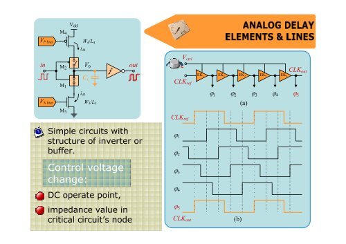
V P bias<br />
V dd<br />
M 4<br />
M 2<br />
V 0<br />
M 1<br />
i d3<br />
W 4 /L 4<br />
i d4<br />
V ctrl<br />
in<br />
out<br />
C L<br />
V N bias<br />
M 3<br />
W 3 /L 3<br />
CLK ref<br />
1 2 3 4 5<br />
CLK ref<br />
EK 1 EK 2 EK 3 EK 4 EK 5<br />
CLK out<br />
(a)<br />
Simple circuits with<br />
structure <strong>of</strong> inverter or<br />
buffer.<br />
Control voltage<br />
change:<br />
DC operate point,<br />
impedance value in<br />
critical circuit’s node<br />
1<br />
2<br />
3<br />
4<br />
5<br />
CLK out<br />
(b)