P89V51RB2/RC2/RD2 8-bit 80C51 5 V low power 16/32 ... - NetMedia
P89V51RB2/RC2/RD2 8-bit 80C51 5 V low power 16/32 ... - NetMedia
P89V51RB2/RC2/RD2 8-bit 80C51 5 V low power 16/32 ... - NetMedia

Create successful ePaper yourself
Turn your PDF publications into a flip-book with our unique Google optimized e-Paper software.
NXP Semiconductors<br />
<strong>P89V51RB2</strong>/<strong>RC2</strong>/<strong>RD2</strong><br />
8-<strong>bit</strong> microcontrollers with <strong>80C51</strong> core<br />
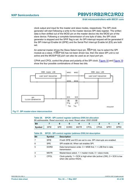
clock output and input for the master and slave modes, respectively. The SPI clock<br />
generator will start fol<strong>low</strong>ing a write to the master devices SPI data register. The written<br />
data is then shifted out of the MOSI pin on the master device into the MOSI pin of the<br />
slave device. Fol<strong>low</strong>ing a complete transmission of one byte of data, the SPI clock<br />
generator is stopped and the SPIF flag is set. An SPI interrupt request will be generated if<br />
the SPI Interrupt Enable <strong>bit</strong> (SPIE) and the Serial Port Interrupt Enable <strong>bit</strong> (ES) are both<br />
set.<br />
An external master drives the Slave Select input pin, SS/P1[4], <strong>low</strong> to select the SPI<br />
module as a slave. If SS/P1[4] has not been driven <strong>low</strong>, then the slave SPI unit is not<br />
active and the MOSI/P1[5] port can also be used as an input port pin.<br />
CPHA and CPOL control the phase and polarity of the SPI clock. Figure 18 and Figure 19<br />
show the four possible combinations of these two <strong>bit</strong>s.<br />
MSB master LSB<br />
MISO<br />
MISO<br />
MSB slave LSB<br />
8-BIT SHIFT REGISTER<br />
8-BIT SHIFT REGISTER<br />
MOSI<br />
MOSI<br />
SPI<br />
CLOCK GENERATOR<br />
SCK<br />
SS<br />
SCK<br />
SS<br />
V DD<br />
V SS<br />
002aaa528<br />
Fig 17. SPI master-slave interconnection<br />
Table 28. SPCR - SPI control register (address D5H) <strong>bit</strong> allocation<br />
Bit addressable; Reset source(s): any reset; Reset value: 0000 0000B<br />
Bit 7 6 5 4 3 2 1 0<br />
Symbol SPIE SPE DORD MSTR CPOL CPHA SPR1 SPR0<br />
Table 29. SPCR - SPI control register (address D5H) <strong>bit</strong> description<br />
Bit Symbol Description<br />
7 SPIE If both SPIE and ES are set to one, SPI interrupts are enabled.<br />
6 SPE SPI enable <strong>bit</strong>. When set enables SPI.<br />
5 DORD Data transmission order. 0 = MSB first; 1 = LSB first in data<br />
transmission.<br />
4 MSTR Master/slave select. 1 = master mode, 0 = slave mode.<br />
3 CPOL Clock polarity. 1 = SCK is high when idle (active LOW), 0 = SCK is <strong>low</strong><br />
when idle (active HIGH).<br />
<strong>P89V51RB2</strong>_<strong>RC2</strong>_<strong>RD2</strong>_4<br />
© NXP B.V. 2007. All rights reserved.<br />
Product data sheet Rev. 04 — 1 May 2007 43 of 80