P89V51RB2/RC2/RD2 8-bit 80C51 5 V low power 16/32 ... - NetMedia
P89V51RB2/RC2/RD2 8-bit 80C51 5 V low power 16/32 ... - NetMedia
P89V51RB2/RC2/RD2 8-bit 80C51 5 V low power 16/32 ... - NetMedia

You also want an ePaper? Increase the reach of your titles
YUMPU automatically turns print PDFs into web optimized ePapers that Google loves.
NXP Semiconductors<br />
<strong>P89V51RB2</strong>/<strong>RC2</strong>/<strong>RD2</strong><br />
8-<strong>bit</strong> microcontrollers with <strong>80C51</strong> core<br />
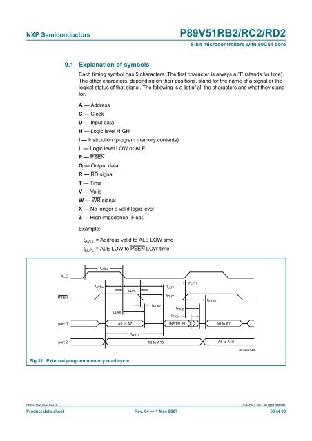
9.1 Explanation of symbols<br />
Each timing symbol has 5 characters. The first character is always a ‘T’ (stands for time).<br />
The other characters, depending on their positions, stand for the name of a signal or the<br />
logical status of that signal. The fol<strong>low</strong>ing is a list of all the characters and what they stand<br />
for.<br />
A — Address<br />
C — Clock<br />
D — Input data<br />
H — Logic level HIGH<br />
I — Instruction (program memory contents)<br />
L — Logic level LOW or ALE<br />
P — PSEN<br />
Q — Output data<br />
R — RD signal<br />
T — Time<br />
V — Valid<br />
W — WR signal<br />
X — No longer a valid logic level<br />
Z — High impedance (Float)<br />
Example:<br />
t AVLL = Address valid to ALE LOW time<br />
t LLPL = ALE LOW to PSEN LOW time<br />
ALE<br />
t LHLL<br />
t AVLL<br />
t LLPL<br />
tLLIV<br />
t PLPH<br />
PSEN<br />
t PLIV<br />
t PXAV<br />
t LLAX<br />
t PLAZ<br />
t PXIZ<br />
t PXIX<br />
port 0<br />
A0 to A7<br />
INSTR IN<br />
A0 to A7<br />
t AVIV<br />
port 2<br />
A8 to A15<br />
A8 to A15<br />
002aaa548<br />
Fig 31. External program memory read cycle<br />
<strong>P89V51RB2</strong>_<strong>RC2</strong>_<strong>RD2</strong>_4<br />
© NXP B.V. 2007. All rights reserved.<br />
Product data sheet Rev. 04 — 1 May 2007 66 of 80