NPN Darlington silicon power transistor - Futurlec
NPN Darlington silicon power transistor - Futurlec
NPN Darlington silicon power transistor - Futurlec

You also want an ePaper? Increase the reach of your titles
YUMPU automatically turns print PDFs into web optimized ePapers that Google loves.
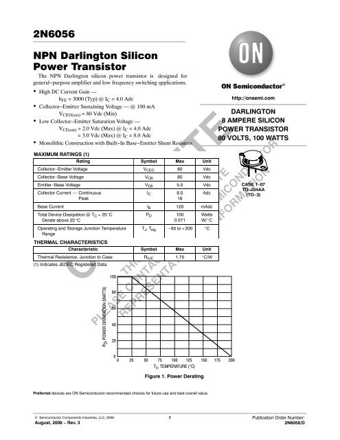
2N6056<br />
<strong>NPN</strong> <strong>Darlington</strong> Silicon<br />
Power Transistor<br />
The <strong>NPN</strong> <strong>Darlington</strong> <strong>silicon</strong> <strong>power</strong> <strong>transistor</strong> is designed for<br />
general−purpose amplifier and low frequency switching applications.<br />
• High DC Current Gain —<br />
h FE = 3000 (Typ) @ I C = 4.0 Adc<br />
• Collector−Emitter Sustaining Voltage — @ 100 mA<br />
V CEO(sus) = 80 Vdc (Min)<br />
• Low Collector−Emitter Saturation Voltage —<br />
V CE(sat) = 2.0 Vdc (Max) @ I C = 4.0 Adc<br />
= 3.0 Vdc (Max) @ I C = 8.0 Adc<br />
• Monolithic Construction with Built−In Base−Emitter Shunt Resistors<br />
http://onsemi.com<br />
DARLINGTON<br />
8 AMPERE SILICON<br />
POWER TRANSISTOR<br />
80 VOLTS, 100 WATTS<br />
MAXIMUM RATINGS (1)<br />
Rating<br />
Symbol<br />
ÎÎÎÎÎÎÎÎÎÎÎÎÎÎÎÎÎÎÎÎÎÎÎ<br />
ÎÎÎÎÎÎÎÎÎÎÎÎÎÎÎÎÎÎÎÎÎÎÎ<br />
Collector−Emitter Voltage ÎÎÎÎÎ<br />
V ÎÎÎÎÎÎÎÎÎÎÎÎÎ CEO ÎÎÎÎ 80 ÎÎÎÎ<br />
Vdc<br />
ÎÎÎÎÎÎÎÎÎÎÎÎÎ<br />
Collector−Base Voltage<br />
ÎÎÎÎÎÎÎÎ<br />
80 ÎÎÎÎ Vdc<br />
Emitter−Base Voltage<br />
ÎÎÎÎÎ<br />
V ÎÎÎÎÎÎÎÎÎÎÎÎÎ EB ÎÎÎÎ 5.0 ÎÎÎÎ<br />
Vdc<br />
ÎÎÎÎÎÎÎÎÎÎÎÎÎÎÎÎÎÎÎÎÎÎÎ<br />
Collector Current — Continuous<br />
Peak<br />
Base Current<br />
ÎÎÎÎÎ<br />
I ÎÎÎÎ<br />
ÎÎÎÎÎÎÎÎÎÎÎÎÎ<br />
B<br />
120 mAdc<br />
ÎÎÎÎ<br />
ÎÎÎÎÎÎÎÎÎÎÎÎÎÎÎÎÎÎÎÎÎÎÎ<br />
Total Device Dissipation @ T C = 25C<br />
Derate above 25C<br />
ÎÎÎÎÎÎÎÎÎÎÎÎÎ ÎÎÎÎ<br />
ÎÎÎÎÎ ÎÎÎÎ<br />
ÎÎÎÎÎÎÎÎÎÎÎÎÎÎÎÎÎ<br />
T J , T stg – 65 to 200ÎÎÎÎ<br />
+ C<br />
ÎÎÎÎ<br />
Operating and Storage Junction Temperature<br />
Range<br />
THERMAL CHARACTERISTICS<br />
Characteristic<br />
V CB<br />
I C<br />
P D<br />
Symbol<br />
Max<br />
8.0<br />
16<br />
100<br />
0.571<br />
Unit<br />
Adc<br />
Watts<br />
W/C<br />
ÎÎÎÎÎÎÎÎÎÎÎÎÎÎÎÎÎÎÎÎÎÎÎ<br />
ÎÎÎÎÎÎÎÎÎÎÎÎÎÎÎÎÎÎÎÎÎÎÎ<br />
Thermal Resistance, Junction to Case<br />
(1) Indicates JEDEC Registered Data<br />
ÎÎÎÎ<br />
ÎÎÎÎÎÎÎÎÎÎÎÎÎÎÎÎÎÎÎÎ<br />
R θJC<br />
Max<br />
Unit<br />
1.75 C/W<br />
ÎÎÎÎ<br />
CASE 1−07<br />
TO−204AA<br />
(TO−3)<br />
ÎÎÎÎÎÎÎÎÎÎÎÎÎ<br />
ÎÎÎÎ<br />
ÎÎÎÎÎ<br />
100<br />
ÎÎÎÎ<br />
PD, POWER DISSIPATION (WATTS)<br />
80<br />
60<br />
40<br />
20<br />
0<br />
0 25 50 75 100 125 150 175 200<br />
T C , TEMPERATURE (°C)<br />
Figure 1. Power Derating<br />
Preferred devices are ON Semiconductor recommended choices for future use and best overall value.<br />
© Semiconductor Components Industries, LLC, 2006<br />
August, 2006 − Rev. 3<br />
1 Publication Order Number:<br />
2N6056/D
2N6056<br />
*ELECTRICAL CHARACTERISTICS (T C = 25C unless otherwise noted)<br />
ÎÎÎÎÎÎÎÎÎÎÎÎÎÎÎÎÎÎÎÎÎÎÎÎÎÎÎÎÎÎÎÎÎ<br />
Characteristic<br />
Symbol<br />
Min Max Unit<br />
ÎÎÎÎÎÎÎÎÎÎÎÎÎÎÎÎÎÎÎÎÎÎÎÎÎÎÎÎÎÎÎÎÎ<br />
OFF CHARACTERISTICS<br />
Collector−Emitter Sustaining Voltage (2)<br />
(I C = 100 mAdc, I B = 0)<br />
V CEO(sus)<br />
ÎÎÎÎÎÎÎÎÎÎÎÎÎÎÎÎÎÎÎÎÎÎÎÎÎÎÎÎÎÎÎÎÎ<br />
ÎÎÎÎÎÎÎÎÎÎÎÎÎÎÎÎÎÎÎÎÎÎÎÎÎÎÎÎÎÎÎÎÎ<br />
Collector Cutoff Current<br />
(V CE = 40 Vdc, I B = 0)<br />
ÎÎÎÎÎÎÎÎÎÎÎÎÎÎÎÎÎÎÎÎÎÎ ÎÎÎÎÎÎÎÎ<br />
ÎÎÎÎÎ<br />
ÎÎÎÎÎÎÎÎÎÎÎÎÎÎÎÎÎÎÎÎÎÎÎÎÎÎÎÎÎÎÎÎÎ<br />
Collector Cutoff Current<br />
(V CE = Rated V CB , V BE(off) = 1.5 Vdc)<br />
(V CE = Rated V CB , V BE(off) = 1.5 Vdc, T C = 150C)<br />
ÎÎÎÎÎÎÎÎÎÎÎÎÎÎÎÎÎÎÎÎÎÎ ÎÎÎÎÎÎÎÎ<br />
ÎÎÎÎÎ<br />
ÎÎÎÎÎÎÎÎÎÎÎÎÎÎÎÎÎÎÎÎÎÎÎÎÎÎÎÎÎÎÎÎÎ<br />
ÎÎÎÎÎÎÎÎÎÎÎÎÎÎÎÎÎÎÎÎÎÎ ÎÎÎÎÎÎÎÎ<br />
ÎÎÎÎÎ<br />
ÎÎÎ<br />
ÎÎÎÎÎÎÎÎÎÎÎÎÎÎÎÎÎÎÎÎÎÎ<br />
Emitter Cutoff Current<br />
ÎÎÎÎÎÎÎ<br />
— ÎÎÎÎmAdc<br />
(V BE = 5.0 Vdc, I C = 0)<br />
ON CHARACTERISTICS (2)<br />
DC Current Gain<br />
(I C = 4.0 Adc, V CE = 3.0 Vdc)<br />
(I C = 8.0 Adc, V CE = 3.0 Vdc)<br />
ÎÎÎÎÎÎÎÎÎÎÎÎÎÎÎÎÎÎÎÎÎÎ ÎÎÎÎÎÎÎÎ<br />
ÎÎÎÎÎ<br />
ÎÎÎÎÎÎÎÎÎÎÎÎÎÎÎÎÎÎÎÎÎÎÎÎÎÎÎÎÎÎÎÎÎ<br />
I CEO<br />
I CEX<br />
I EBO<br />
80<br />
—<br />
—<br />
—<br />
—<br />
0.5<br />
0.5<br />
5.0<br />
Vdc<br />
mAdc<br />
mAdc<br />
2.0 ÎÎÎ<br />
ÎÎÎÎÎÎÎÎÎÎÎÎÎÎÎÎÎÎÎÎÎÎÎÎÎÎÎÎÎÎÎÎÎ<br />
ÎÎÎÎÎÎ<br />
ÎÎÎ<br />
ÎÎÎÎÎ<br />
ÎÎÎÎÎÎÎÎÎÎÎÎÎÎÎÎÎÎÎÎÎÎ<br />
Collector−Emitter Saturation Voltage<br />
(I C = 4.0 Adc, I B = 16 mAdc)<br />
(I C = 8.0 Adc, I B = 80 mAdc)<br />
ÎÎÎÎÎÎÎÎÎÎÎÎÎÎÎÎÎÎÎÎÎÎ<br />
ÎÎÎÎÎÎÎ<br />
ÎÎÎÎÎÎ<br />
ÎÎÎÎÎÎ<br />
ÎÎÎ<br />
ÎÎÎÎÎ<br />
ÎÎÎÎÎÎÎÎÎÎÎÎÎÎÎÎÎÎÎÎÎÎ<br />
h FE<br />
V CE(sat)<br />
750<br />
100<br />
18000<br />
—<br />
ÎÎÎÎÎÎÎÎÎÎÎÎÎÎÎÎÎÎÎÎÎÎ<br />
Base−Emitter Saturation Voltage<br />
ÎÎÎÎÎ<br />
V ÎÎÎ<br />
BE(sat) — 4.0<br />
ÎÎÎ<br />
Vdc<br />
ÎÎÎÎÎÎ<br />
ÎÎÎÎ<br />
ÎÎÎ<br />
ÎÎÎÎÎ<br />
ÎÎÎÎÎÎÎÎÎÎÎÎÎÎÎÎÎÎÎÎÎÎ<br />
(I C = 8.0 Adc, I B = 80 mAdc)<br />
ÎÎÎÎÎÎÎÎÎÎÎÎÎÎÎÎÎÎÎÎÎÎ<br />
Base−Emitter On ÎÎÎÎÎ<br />
Voltage<br />
V BE(on) ÎÎÎÎÎÎÎÎ<br />
— Vdc<br />
ÎÎÎÎÎÎÎÎÎÎÎÎÎÎÎÎÎÎÎÎÎÎ<br />
(I C = 4.0 Adc, V CE<br />
ÎÎÎ<br />
ÎÎÎÎ<br />
ÎÎÎ<br />
ÎÎÎÎÎ<br />
= 3.0 Vdc)<br />
DYNAMIC CHARACTERISTICS<br />
ÎÎÎÎÎÎÎÎÎÎÎÎÎÎÎÎÎÎÎÎÎÎÎÎÎÎÎÎÎÎÎÎÎ<br />
Magnitude of Common Emitter Small−Signal Short Circuit Current Transfer Ratio<br />
(I C = 3.0 Adc, V CE = 3.0 Vdc, f =<br />
ÎÎÎÎÎ<br />
|h fe |<br />
ÎÎÎ<br />
4.0 —<br />
ÎÎÎÎÎÎ<br />
—<br />
1.0 MHz)<br />
—<br />
—<br />
2.0<br />
3.0<br />
—<br />
Vdc<br />
2.8 ÎÎÎ<br />
ÎÎÎÎÎÎÎÎÎÎÎÎÎÎÎÎÎÎÎÎÎÎÎÎÎÎÎÎÎÎÎÎÎ<br />
ÎÎÎÎÎÎÎÎÎÎÎÎÎÎÎÎÎÎÎÎÎÎ<br />
Output Capacitance<br />
ÎÎÎÎÎ<br />
C ÎÎÎ ÎÎÎ<br />
ob — pF<br />
ÎÎÎÎ<br />
ÎÎÎÎÎÎ<br />
ÎÎÎ<br />
ÎÎÎÎÎ<br />
ÎÎÎÎÎÎÎÎÎÎÎÎÎÎÎÎÎÎÎÎÎÎ<br />
(V CB = 10 Vdc, I E = 0, f = 0.1 MHz)<br />
200 ÎÎÎ<br />
ÎÎÎÎÎÎÎÎÎÎÎÎÎÎÎÎÎÎÎÎÎÎ<br />
Small−Signal Current ÎÎÎÎÎ<br />
Gain<br />
h fe<br />
300 — ÎÎÎ<br />
ÎÎÎ<br />
— ÎÎÎÎ<br />
(I C = 3.0 Adc, V CE<br />
ÎÎÎÎÎÎ<br />
ÎÎÎ<br />
ÎÎÎÎÎ<br />
= 3.0 Vdc, f = 1.0 kHz)<br />
ÎÎÎÎÎÎÎÎÎÎÎÎÎÎÎÎÎÎÎÎÎÎ<br />
*Indicates JEDEC Registered Data.<br />
(2) Pulse Test: Pulse Width = 300 μs, Duty Cycle = 2.0%<br />
http://onsemi.com<br />
2
2N6056<br />
R B & R C VARIED TO OBTAIN DESIRED CURRENT LEVELS<br />
D 1 MUST BE FAST RECOVERY TYPE, e.g.,<br />
1N5825 USED ABOVE I B ≈ 100 mA<br />
MSD6100 USED BELOW I B ≈ 100 mA<br />
V 2<br />
approx<br />
+12 V<br />
0<br />
V 1<br />
approx<br />
−8.0 V<br />
t r , t f ≤ 10 ns<br />
DUTY CYCLE = 1.0%<br />
25 μs<br />
51<br />
Figure 2. Switching Times Test Circuit<br />
R B<br />
D 1<br />
+4.0 V<br />
R C<br />
TUT<br />
≈ 8.0 k ≈ 50<br />
for t d and t r , D 1 is disconnected<br />
and V 2 = 0<br />
V CC<br />
−30 V<br />
SCOPE<br />
For <strong>NPN</strong> test circuit reverse diode, polarities and input pulses.<br />
t, TIME (s) μ<br />
5.0<br />
3.0<br />
2.0<br />
1.0<br />
0.7<br />
0.5<br />
0.3<br />
0.2<br />
0.1<br />
0.07<br />
0.05<br />
0.1<br />
V CC = 30 V<br />
I C /I B = 250<br />
I B1 = I B2<br />
T J = 25°C<br />
t s<br />
t d @ V BE(off) = 0<br />
0.2 0.3 0.5 0.7 1.0 2.0 3.0 5.0 7.0 10<br />
I C , COLLECTOR CURRENT (AMP)<br />
Figure 3. Switching Times<br />
t f<br />
t r<br />
1.0<br />
0.7<br />
0.5<br />
D = 0.5<br />
r(t), TRANSIENT THERMAL<br />
RESISTANCE (NORMALIZED)<br />
0.3<br />
0.2<br />
0.1<br />
0.07<br />
0.05<br />
0.03<br />
0.02<br />
0.2<br />
0.1<br />
0.05<br />
0.02<br />
0.01<br />
SINGLE PULSE<br />
R θJC (t) = r(t) R θJC<br />
R θJC = 1.75°C/W 2N6056<br />
D CURVES APPLY FOR POWER<br />
PULSE TRAIN SHOWN<br />
READ TIME AT t 1<br />
T J(pk) − T C = P (pk) θ JC (t)<br />
P (pk)<br />
t 1<br />
t 2<br />
DUTY CYCLE, D = t 1 /t 2<br />
0.01 0.1<br />
0.2 0.3 0.5 0.7 1.0 2.0 3.0 5.0 7.0 10 20 30 50 70 100 200 300 500 700 1000<br />
t, TIME (ms)<br />
Figure 4. Thermal Response<br />
http://onsemi.com<br />
3
2N6056<br />
ACTIVE−REGION SAFE OPERATING AREA<br />
I C , COLLECTOR CURRENT (AMP)<br />
50<br />
20<br />
10<br />
5.0<br />
2.0<br />
1.0<br />
0.5<br />
0.2<br />
0.1<br />
0.05<br />
1.0<br />
T J = 200°C<br />
0.5 ms<br />
1.0 ms<br />
5.0 ms<br />
SECOND BREAKDOWN LIMIT<br />
BONDING WIRE LIMIT<br />
THERMALLY LIMITED<br />
@ T C = 25°C (SINGLE PULSE)<br />
2.0 3.0 5.0 7.0 10 20 30 50 70 100<br />
V CE , COLLECTOR−EMITTER VOLTAGE (VOLTS)<br />
dc<br />
Figure 5. Safe Operating Area<br />
0.1 ms<br />
There are two limitations on the <strong>power</strong> handling ability of<br />
a <strong>transistor</strong>: average junction temperature and second<br />
breakdown. Safe operating area curves indicate I C − V CE<br />
limits of the <strong>transistor</strong> that must be observed for reliable<br />
operation; i.e., the <strong>transistor</strong> must not be subjected to greater<br />
dissipation than the curves indicate.<br />
The data of Figure 5 is based on T J(pk) = 200C;<br />
T C is variable depending on conditions. Second breakdown<br />
pulse limits are valid for duty cycles to 10% provided T J(pk)<br />
200C. T J(pk) may be calculated from the data in<br />
Figure 4. At high case temperatures, thermal limitations will<br />
reduce the <strong>power</strong> that can be handled to values less than the<br />
limitations imposed by second breakdown.<br />
hfe , SMALL−SIGNAL CURRENT GAIN<br />
10,000<br />
5000<br />
3000<br />
2000<br />
1000<br />
500<br />
300<br />
200<br />
100<br />
50<br />
30<br />
20<br />
10<br />
1.0<br />
T C = 25°C<br />
V CE = 3.0 Vdc<br />
I C = 3.0 Adc<br />
300<br />
30<br />
2.0 5.0 10 20 50 100 200 500 1000 0.1 0.2 0.5 1.0 2.0 5.0 10 20 50 100<br />
f, FREQUENCY (kHz)<br />
V R , REVERSE VOLTAGE (VOLTS)<br />
Figure 6. Small−Signal Current Gain<br />
C, CAPACITANCE (pF)<br />
200<br />
100<br />
70<br />
50<br />
C ib<br />
C ob<br />
Figure 7. Capacitance<br />
T J = 25°C<br />
http://onsemi.com<br />
4
2N6056<br />
hFE, DC CURRENT GAIN<br />
20,000<br />
10,000<br />
5000<br />
3000<br />
2000<br />
1000<br />
500<br />
300<br />
200<br />
0.1<br />
T J = 150°C<br />
25°C<br />
−55 °C<br />
I C , COLLECTOR CURRENT (AMP)<br />
V CE = 3.0 V<br />
VCE, COLLECTOR−EMITTER VOLTAGE (VOLTS)<br />
3.0<br />
2.6<br />
2.2<br />
1.8<br />
1.4<br />
I C = 2.0 A 4.0 A 6.0 A<br />
I B , BASE CURRENT (mA)<br />
T J = 25°C<br />
1.0<br />
0.2 0.3 0.5 0.7 1.0 2.0 3.0 5.0 7.0 10 0.3 0.5 0.7 1.0 2.0 3.0 5.0 7.0 10 20 30<br />
Figure 8. DC Current Gain<br />
Figure 9. Collector Saturation Region<br />
3.0<br />
2.5<br />
T J = 25°C<br />
V, VOLTAGE (VOLTS)<br />
2.0<br />
1.5<br />
1.0<br />
V BE @ V CE = 3.0 V<br />
V BE(sat) @ I C /I B = 250<br />
V CE(sat) @ I C /I B = 250<br />
0.5<br />
0.1 0.2 0.3 0.5 0.7 1.0 2.0 3.0 5.0 7.0 10<br />
I C , COLLECTOR CURRENT (AMP)<br />
Figure 10. “On” Voltage<br />
http://onsemi.com<br />
5
2N6056<br />
PACKAGE DIMENSIONS<br />
CASE 1−07<br />
TO−204AA (TO−3)<br />
ISSUE Z<br />
V<br />
H<br />
E<br />
2<br />
1<br />
A<br />
N<br />
C<br />
−T− SEATING<br />
PLANE<br />
D 2 PL K<br />
0.13 (0.005) M T Q M Y M<br />
U<br />
L −Y−<br />
G B<br />
−Q−<br />
0.13 (0.005) M T<br />
Y<br />
M<br />
NOTES:<br />
1. DIMENSIONING AND TOLERANCING PER ANSI<br />
Y14.5M, 1982.<br />
2. CONTROLLING DIMENSION: INCH.<br />
3. ALL RULES AND NOTES ASSOCIATED WITH<br />
REFERENCED TO−204AA OUTLINE SHALL APPLY.<br />
INCHES MILLIMETERS<br />
DIM MIN MAX MIN MAX<br />
A 1.550 REF 39.37 REF<br />
B −−− 1.050 −−− 26.67<br />
C 0.250 0.335 6.35 8.51<br />
D 0.038 0.043 0.97 1.09<br />
E 0.055 0.070 1.40 1.77<br />
G 0.430 BSC 10.92 BSC<br />
H 0.215 BSC 5.46 BSC<br />
K 0.440 0.480 11.18 12.19<br />
L 0.665 BSC 16.89 BSC<br />
N −−− 0.830 −−− 21.08<br />
Q 0.151 0.165 3.84 4.19<br />
U 1.187 BSC 30.15 BSC<br />
V 0.131 0.188 3.33 4.77<br />
STYLE 1:<br />
PIN 1. BASE<br />
2. EMITTER<br />
CASE: COLLECTOR<br />
ON Semiconductor and are registered trademarks of Semiconductor Components Industries, LLC (SCILLC). SCILLC reserves the right to make changes without further notice<br />
to any products herein. SCILLC makes no warranty, representation or guarantee regarding the suitability of its products for any particular purpose, nor does SCILLC assume any liability<br />
arising out of the application or use of any product or circuit, and specifically disclaims any and all liability, including without limitation special, consequential or incidental damages.<br />
“Typical” parameters which may be provided in SCILLC data sheets and/or specifications can and do vary in different applications and actual performance may vary over time. All<br />
operating parameters, including “Typicals” must be validated for each customer application by customer’s technical experts. SCILLC does not convey any license under its patent rights<br />
nor the rights of others. SCILLC products are not designed, intended, or authorized for use as components in systems intended for surgical implant into the body, or other applications<br />
intended to support or sustain life, or for any other application in which the failure of the SCILLC product could create a situation where personal injury or death may occur. Should<br />
Buyer purchase or use SCILLC products for any such unintended or unauthorized application, Buyer shall indemnify and hold SCILLC and its officers, employees, subsidiaries, affiliates,<br />
and distributors harmless against all claims, costs, damages, and expenses, and reasonable attorney fees arising out of, directly or indirectly, any claim of personal injury or death<br />
associated with such unintended or unauthorized use, even if such claim alleges that SCILLC was negligent regarding the design or manufacture of the part. SCILLC is an Equal<br />
Opportunity/Affirmative Action Employer. This literature is subject to all applicable copyright laws and is not for resale in any manner.<br />
PUBLICATION ORDERING INFORMATION<br />
LITERATURE FULFILLMENT:<br />
Literature Distribution Center for ON Semiconductor<br />
P.O. Box 5163, Denver, Colorado 80217 USA<br />
Phone: 303−675−2175 or 800−344−3860 Toll Free USA/Canada<br />
Fax: 303−675−2176 or 800−344−3867 Toll Free USA/Canada<br />
Email: orderlit@onsemi.com<br />
N. American Technical Support: 800−282−9855 Toll Free<br />
USA/Canada<br />
Europe, Middle East and Africa Technical Support:<br />
Phone: 421 33 790 2910<br />
Japan Customer Focus Center<br />
Phone: 81−3−5773−3850<br />
http://onsemi.com<br />
6<br />
ON Semiconductor Website: www.onsemi.com<br />
Order Literature: http://www.onsemi.com/orderlit<br />
For additional information, please contact your local<br />
Sales Representative<br />
2N6056/D