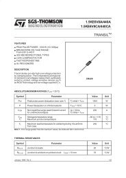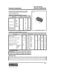
NPN Darlington silicon power transistor - Futurlec
NPN Darlington silicon power transistor - Futurlec
NPN Darlington silicon power transistor - Futurlec

You also want an ePaper? Increase the reach of your titles
YUMPU automatically turns print PDFs into web optimized ePapers that Google loves.
2N6056<br />
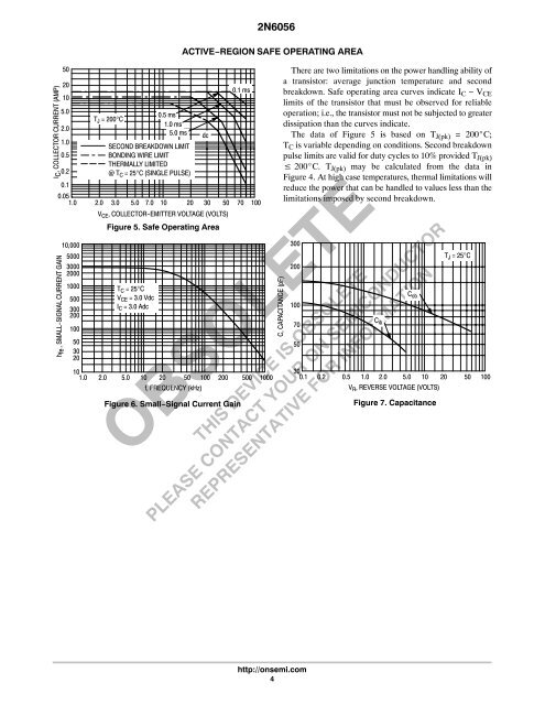
ACTIVE−REGION SAFE OPERATING AREA<br />
I C , COLLECTOR CURRENT (AMP)<br />
50<br />
20<br />
10<br />
5.0<br />
2.0<br />
1.0<br />
0.5<br />
0.2<br />
0.1<br />
0.05<br />
1.0<br />
T J = 200°C<br />
0.5 ms<br />
1.0 ms<br />
5.0 ms<br />
SECOND BREAKDOWN LIMIT<br />
BONDING WIRE LIMIT<br />
THERMALLY LIMITED<br />
@ T C = 25°C (SINGLE PULSE)<br />
2.0 3.0 5.0 7.0 10 20 30 50 70 100<br />
V CE , COLLECTOR−EMITTER VOLTAGE (VOLTS)<br />
dc<br />
Figure 5. Safe Operating Area<br />
0.1 ms<br />
There are two limitations on the <strong>power</strong> handling ability of<br />
a <strong>transistor</strong>: average junction temperature and second<br />
breakdown. Safe operating area curves indicate I C − V CE<br />
limits of the <strong>transistor</strong> that must be observed for reliable<br />
operation; i.e., the <strong>transistor</strong> must not be subjected to greater<br />
dissipation than the curves indicate.<br />
The data of Figure 5 is based on T J(pk) = 200C;<br />
T C is variable depending on conditions. Second breakdown<br />
pulse limits are valid for duty cycles to 10% provided T J(pk)<br />
200C. T J(pk) may be calculated from the data in<br />
Figure 4. At high case temperatures, thermal limitations will<br />
reduce the <strong>power</strong> that can be handled to values less than the<br />
limitations imposed by second breakdown.<br />
hfe , SMALL−SIGNAL CURRENT GAIN<br />
10,000<br />
5000<br />
3000<br />
2000<br />
1000<br />
500<br />
300<br />
200<br />
100<br />
50<br />
30<br />
20<br />
10<br />
1.0<br />
T C = 25°C<br />
V CE = 3.0 Vdc<br />
I C = 3.0 Adc<br />
300<br />
30<br />
2.0 5.0 10 20 50 100 200 500 1000 0.1 0.2 0.5 1.0 2.0 5.0 10 20 50 100<br />
f, FREQUENCY (kHz)<br />
V R , REVERSE VOLTAGE (VOLTS)<br />
Figure 6. Small−Signal Current Gain<br />
C, CAPACITANCE (pF)<br />
200<br />
100<br />
70<br />
50<br />
C ib<br />
C ob<br />
Figure 7. Capacitance<br />
T J = 25°C<br />
http://onsemi.com<br />
4