Towards 2020 – Photonics driving economic growth in Europe

Create successful ePaper yourself
Turn your PDF publications into a flip-book with our unique Google optimized e-Paper software.
2. <strong>Photonics</strong> Research and Innovation Challenges<br />
61<br />
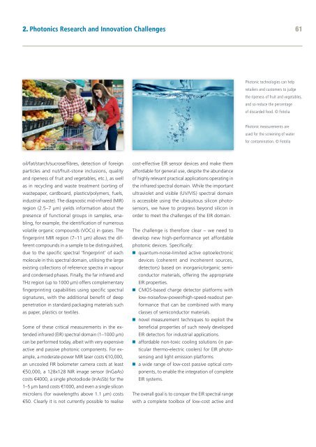
Photonic technologies can help<br />
retailers and customers to judge<br />
the ripeness of fruit and vegetables,<br />
and so reduce the percentage<br />
of discarded food. © Fotolia<br />
Photonic measurements are<br />
used for the screen<strong>in</strong>g of water<br />
for contam<strong>in</strong>ation. © Fotolia<br />
oil/fat/starch/sucrose/fibres, detection of foreign<br />
particles and nut/fruit-stone <strong>in</strong>clusions, quality<br />
and ripeness of fruit and vegetables, etc.), as well<br />
as <strong>in</strong> recycl<strong>in</strong>g and waste treatment (sort<strong>in</strong>g of<br />
wastepaper, cardboard, plastics/polymers, fuels,<br />
<strong>in</strong>dustrial waste). The diagnostic mid-<strong>in</strong>frared (MIR)<br />
region (2.5<strong>–</strong>7 µm) yields <strong>in</strong>formation about the<br />
presence of functional groups <strong>in</strong> samples, enabl<strong>in</strong>g,<br />
for example, the identification of numerous<br />
volatile organic compounds (VOCs) <strong>in</strong> gases. The<br />
f<strong>in</strong>gerpr<strong>in</strong>t MIR region (7<strong>–</strong>11 µm) allows the different<br />
compounds <strong>in</strong> a sample to be dist<strong>in</strong>guished,<br />
due to the specific spectral ‘f<strong>in</strong>gerpr<strong>in</strong>t’ of each<br />
molecule <strong>in</strong> this spectral doma<strong>in</strong>, utilis<strong>in</strong>g the large<br />
exist<strong>in</strong>g collections of reference spectra <strong>in</strong> vapour<br />
and condensed phases. F<strong>in</strong>ally, the far <strong>in</strong>frared and<br />
THz region (up to 1000 µm) offers complementary<br />
f<strong>in</strong>gerpr<strong>in</strong>t<strong>in</strong>g capabilities us<strong>in</strong>g specific spectral<br />
signatures, with the additional benefit of deep<br />
penetration <strong>in</strong> standard packag<strong>in</strong>g materials such<br />
as paper, plastics or textiles.<br />
Some of these critical measurements <strong>in</strong> the extended<br />
<strong>in</strong>frared (EIR) spectral doma<strong>in</strong> (1<strong>–</strong>1000 µm)<br />
can be performed today, albeit with very expensive<br />
active and passive photonic components. For example,<br />
a moderate-power MIR laser costs €10,000,<br />
an uncooled FIR bolometer camera costs at least<br />
€50,000, a 128x128 NIR image sensor (InGaAs)<br />
costs €4000, a s<strong>in</strong>gle photodiode (InAsSb) for the<br />
1<strong>–</strong>5 µm band costs €1000, and even a s<strong>in</strong>gle silicon<br />
microlens (for wavelengths above 1.1 µm) costs<br />
€50. Clearly it is not currently possible to realise<br />
cost-effective EIR sensor devices and make them<br />
affordable for general use, despite the abundance<br />
of highly relevant practical applications operat<strong>in</strong>g <strong>in</strong><br />
the <strong>in</strong>frared spectral doma<strong>in</strong>. While the important<br />
ultraviolet and visible (UV/VIS) spectral doma<strong>in</strong><br />
is accessible us<strong>in</strong>g the ubiquitous silicon photosensors,<br />
we have to progress beyond silicon <strong>in</strong><br />
order to meet the challenges of the EIR doma<strong>in</strong>.<br />
The challenge is therefore clear <strong>–</strong> we need to<br />
develop new high-performance yet affordable<br />
photonic devices. Specifically:<br />
n quantum-noise-limited active optoelectronic<br />
devices (coherent and <strong>in</strong>coherent sources,<br />
detectors) based on <strong>in</strong>organic/organic semiconductor<br />
materials, offer<strong>in</strong>g the appropriate<br />
EIR properties.<br />
n CMOS-based charge detector platforms with<br />
low-noise/low-power/high-speed-readout performance<br />
that can be comb<strong>in</strong>ed with many<br />
classes of semiconductor materials.<br />
n novel measurement techniques to exploit the<br />
beneficial properties of such newly developed<br />
EIR detectors for <strong>in</strong>dustrial applications.<br />
n affordable non-toxic cool<strong>in</strong>g solutions (<strong>in</strong> particular<br />
thermo-electric coolers) for EIR photosens<strong>in</strong>g<br />
and light emission platforms<br />
n a wide range of low-cost passive optical components,<br />
to enable the <strong>in</strong>tegration of complete<br />
EIR systems.<br />
The overall goal is to conquer the EIR spectral range<br />
with a complete toolbox of low-cost active and