Towards 2020 – Photonics driving economic growth in Europe

Create successful ePaper yourself
Turn your PDF publications into a flip-book with our unique Google optimized e-Paper software.
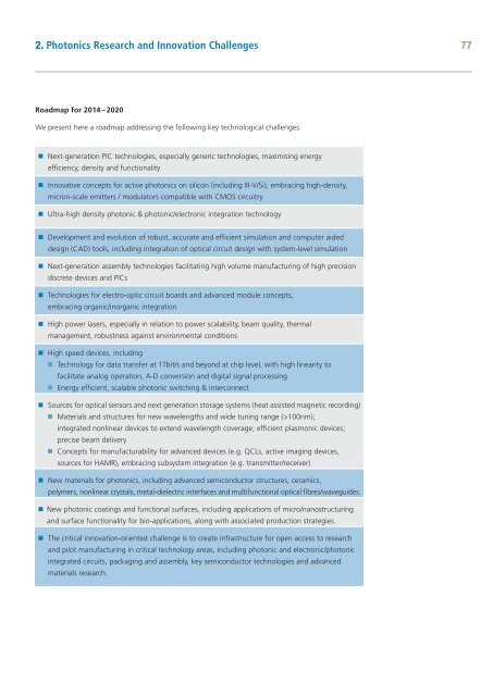
2. <strong>Photonics</strong> Research and Innovation Challenges<br />
77<br />
Roadmap for 2014 <strong>–</strong> <strong>2020</strong><br />
We present here a roadmap address<strong>in</strong>g the follow<strong>in</strong>g key technological challenges:<br />
n Next-generation PIC technologies, especially generic technologies, maximis<strong>in</strong>g energy<br />
efficiency, density and functionality<br />
n Innovative concepts for active photonics on silicon (<strong>in</strong>clud<strong>in</strong>g III-V/Si), embrac<strong>in</strong>g high-density,<br />
micron-scale emitters / modulators compatible with CMOS circuitry<br />
n Ultra-high density photonic & photonic/electronic <strong>in</strong>tegration technology<br />
n Development and evolution of robust, accurate and efficient simulation and computer aided<br />
design (CAD) tools, <strong>in</strong>clud<strong>in</strong>g <strong>in</strong>tegration of optical circuit design with system-level simulation<br />
n Next-generation assembly technologies facilitat<strong>in</strong>g high volume manufactur<strong>in</strong>g of high precision<br />
discrete devices and PICs<br />
n Technologies for electro-optic circuit boards and advanced module concepts,<br />
embrac<strong>in</strong>g organic/<strong>in</strong>organic <strong>in</strong>tegration<br />
n High power lasers, especially <strong>in</strong> relation to power scalability, beam quality, thermal<br />
management, robustness aga<strong>in</strong>st environmental conditions<br />
n High speed devices, <strong>in</strong>clud<strong>in</strong>g<br />
n Technology for data transfer at 1Tbit/s and beyond at chip level, with high l<strong>in</strong>earity to<br />
facilitate analog operation, A-D conversion and digital signal process<strong>in</strong>g<br />
n Energy efficient, scalable photonic switch<strong>in</strong>g & <strong>in</strong>terconnect<br />
n Sources for optical sensors and next generation storage systems (heat assisted magnetic record<strong>in</strong>g)<br />
n Materials and structures for new wavelengths and wide tun<strong>in</strong>g range (>100nm);<br />
<strong>in</strong>tegrated nonl<strong>in</strong>ear devices to extend wavelength coverage; efficient plasmonic devices;<br />
precise beam delivery<br />
n Concepts for manufacturability for advanced devices (e.g. QCLs, active imag<strong>in</strong>g devices,<br />
sources for HAMR), embrac<strong>in</strong>g subsystem <strong>in</strong>tegration (e.g. transmitter/receiver)<br />
n New materials for photonics, <strong>in</strong>clud<strong>in</strong>g advanced semiconductor structures, ceramics,<br />
polymers, nonl<strong>in</strong>ear crystals, metal-dielectric <strong>in</strong>terfaces and multifunctional optical fibres/waveguides.<br />
n New photonic coat<strong>in</strong>gs and functional surfaces, <strong>in</strong>clud<strong>in</strong>g applications of micro/nanostructur<strong>in</strong>g<br />
and surface functionality for bio-applications, along with associated production strategies.<br />
n The critical <strong>in</strong>novation-oriented challenge is to create <strong>in</strong>frastructure for open access to research<br />
and pilot manufactur<strong>in</strong>g <strong>in</strong> critical technology areas, <strong>in</strong>clud<strong>in</strong>g photonic and electronic/photonic<br />
<strong>in</strong>tegrated circuits, packag<strong>in</strong>g and assembly, key semiconductor technologies and advanced<br />
materials research.