- Page 1 and 2:
SDZD001B TheTTL ,Data Book Volume 4
- Page 4:
General Information Functional Inde
- Page 7 and 8:
IMPORTANT NOTICE Texas Instruments
- Page 9 and 10:
G) CD ::::s CD ... ~ ::::s ..... o
- Page 11 and 12:
A new Field Programmable Logic Appl
- Page 13 and 14:
ALPHANUMERIC INDEX RAMs and Memory-
- Page 15 and 16:
GLOSSARY Output-Enable Input A gati
- Page 17 and 18:
GLOSSARY C) CD :::J CD ... ~ .... 5
- Page 19 and 20:
EXPLANATION OF FUNCTION TABLES The
- Page 21 and 22:
SERIES 1 AND 2 PROMs, RAMs, MEMORY
- Page 23 and 24:
SERIES TIBPAL', PAL', TIFPLA DEVICE
- Page 25 and 26:
ORDERING INFORMATION II PROM NUMBER
- Page 27 and 28:
::J -o 3 Q) .-+ o· ::J 1-20
- Page 29 and 30:
HARDWARE/SOFTWARE MANUFACTURERS ADD
- Page 31 and 32:
'T1 c: ::J n ... o· ::J ~ ::J Q, C
- Page 33 and 34:
FUNCTIONAL Ir~DEX GATES, EXPANDERS,
- Page 35 and 36:
FUNCTIONAL INDEX BUFFERS, DRIVERS,
- Page 37 and 38:
FUNCTIONAL INDEX LATCHES AND MUL TI
- Page 39 and 40:
FUNCTIONAL INDEX COUNTERS II "T1 r:
- Page 41 and 42:
FUNCTIONAL INDEX DISPLAY DECODERS/D
- Page 43 and 44:
FUNCTIONAL INDEX ARITHMETIC CIRCUIT
- Page 45 and 46:
FUNCTIONAL INDEX PROGRAMMABLE LOGIC
- Page 47 and 48:
"T1 m· c: ." ""I o cc ""I Q) 3 3 Q
- Page 49 and 50:
PAL16R4A, PAL16R6A, PAL16R8A STANDA
- Page 51 and 52:
PAL 16R6A, PAL 16R8A STANDARD HIGH
- Page 53 and 54:
~ PAL16R4A STANDARD HIGH,SPEED PAL
- Page 55 and 56:
PAL16RBA STANDARD HIGH·SPEED PAL C
- Page 57 and 58:
PAL 16L8A, PAL 16R4A, PAL 16R6A, PA
- Page 59 and 60:
PAL 16L8A, PAL 16R4A, PAL 16R6A, PA
- Page 61 and 62:
3-16
- Page 63 and 64:
PAL20R4A. PAL20R6A. PAL20R8A STANDA
- Page 65 and 66:
PAL20R6A. PAL20R8A STANDARD HIGH SP
- Page 67 and 68:
PAL20R4A STANDARD HIGH SPEED PAL CI
- Page 69 and 70:
PAL20R8A STANDARD HIGH SPEED PAL CI
- Page 71 and 72:
PAL20L8A, PAL20R4A, PAL20R6A, PAL20
- Page 73 and 74:
PAL20L8A, PAL20R4A, PAL20R6A, PAL20
- Page 75 and 76:
PAL20L8A, PAL20R4A, PAL20R6A, PAL20
- Page 77 and 78:
TIBPAL 16R4, TIBPAL 16R6, TIBPAL 16
- Page 79 and 80:
TIBPAL 16R6, TIBPAL 16R8 HIGH·PERF
- Page 81 and 82:
TIBPAL16R4 HIGH·PERFORMANCE IMPACT
- Page 83 and 84:
TIBPAL 16R8 HIGH·PERFORMANCE IMPAC
- Page 85 and 86:
TIBPAL 16LH, TIBPAL 16R4, TIBPAL 16
- Page 87 and 88:
TIBPAL 16L8, TIBPAL 16R4, TIBPAL 16
- Page 89 and 90:
"T1 [ Co ""I o cc ""I Q) 3 3 Q) C"
- Page 91 and 92:
TIBPAL 16R4·12, TIBPAL 16R6·12, T
- Page 93 and 94:
TIBPAL 16R6·12, TIBPAL 16R8·12 12
- Page 95 and 96:
~ TIBPAL 16R4·12 12·NS IMPAcr M P
- Page 97 and 98:
~ TIBPAL 16R8,12 12,NS IMPACr M PAL
- Page 99 and 100:
TIBPAL 16L8·12, TIBPAL 16R4·12, T
- Page 101 and 102:
TIBPAL 16L8·12, TIBPAL 16R4·12, T
- Page 103 and 104:
"T1 [ Co I ""0 ... o cc ... D.l 3 3
- Page 105 and 106:
THCTPAL16L8, THCTPAL16R4, THCTPAL16
- Page 107 and 108:
TIBPAL20R4·15, TIBPAL20R6·15, TIB
- Page 109 and 110:
TIBPAL20R6·15, TIBPAL20R8·15 TIBP
- Page 111 and 112:
'"T1 (1). e: ... -a o cc ... Q) 3 3
- Page 113 and 114: TIBPAL20R8·15 TIBPAL20R8·20 HIGH
- Page 115 and 116: TIBPAL20L8·15, TIBPAL20R4·15, TIB
- Page 117 and 118: TIBPAL20L8·15, TIBPAL20R4·15, TIB
- Page 119 and 120: TIBPAL20X4, TIBPAL20X8, TIBPAL20X10
- Page 121 and 122: TIBPAL20X8, TIBPAL20X10 HIGH·PERFO
- Page 123 and 124: ~ TIBPAL20X4 HIGH·PERFORMANCE EXCL
- Page 125 and 126: TIBPAL20X10 HIGH·PERFORMANCE EXCLU
- Page 127 and 128: TIBPAL20L 10, TIBPAL20X4, TIBPAL20X
- Page 129 and 130: TIBPAL20L 10, TIBPAL20X4, TIBPAL20X
- Page 131 and 132: TlBPAL20L 10, TIBPAL20X4, TlBPAL20X
- Page 133 and 134: TIBPAL20L 10, TIBPAL20X4, TIBPAL20X
- Page 135 and 136: TIBPALR19R4, TIBPALR19R6, TIBPALR19
- Page 137 and 138: TIBPALR19R6, TIBPALR19R8 HIGH·PERF
- Page 139 and 140: TIBPALR19R4 HIGH·PERFORMANCE REGIS
- Page 141 and 142: TIBPALR 19R8 HIGH-PERFORMANCE REGIS
- Page 143 and 144: TIBPALR19L8, TIBPALR19R4, TIBPALR19
- Page 145 and 146: TIBPALR19L8, TIBPALR19R4, TIBPALR19
- Page 147 and 148: TIBPALR19L8, TIBPALR19R4, TIBPALR19
- Page 149 and 150: TIBPALR19L8, TIBPALR19R4, TlBPALR19
- Page 151 and 152: TIBPALT19R4, TIBPALT19R6, TIBPALT19
- Page 153 and 154: TIBPALT19R6, TIBPALT19R8 HIGH·PERF
- Page 155 and 156: TIBPAL T1 9R4 HIGH·PERFORMANCE LAT
- Page 157 and 158: TIBPALT19RB HIGH·PERFORMANCE LATCH
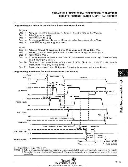
- Page 159 and 160: TIBPALT19L8. TIBPAL T19R4. TIBPAL T
- Page 161 and 162: TIBPALT19L8, TIBPALT19R4, TIBPALT19
- Page 163: TIBPAL T19L8. TIBPALT19R4. TIBPALT1
- Page 167 and 168: TIB82S105B 16 x 48 x 8 FIELD·PROGR
- Page 169 and 170: TIB82S105B 16 x 48 x 8 FIELD·PROGR
- Page 171 and 172: TIB82S105B 16 x 48 x 8 FIELD·PROGR
- Page 173 and 174: TIB82S105B 16 x 48 x 8 FIELD·PROGR
- Page 175 and 176: TIB82S105B 16 x 48 x 8 FIELD·PROGR
- Page 177 and 178: TIB82S1058 16 x 48 x 8 FIELD·PROGR
- Page 179 and 180: TIB82S105B 16 x 48 x 8 FIELD·PROGR
- Page 181 and 182: TIB82S167B 14 >< 48 x 6 FIELD·PROG
- Page 183 and 184: TIB82S167B 14 x 48 x 6 FIELD·PROGR
- Page 185 and 186: TIB82S167B 14 x 48 x 6 FIELD·PROGR
- Page 187 and 188: TIB82S167B 14 x 48 x 6 FIELD·PROGR
- Page 189 and 190: TIB82S167B 14 X 48 X 6 FIELD·PROGR
- Page 191 and 192: TIB82S167B 14 x 48 x 6 FIELD-PROGRA
- Page 193 and 194: ." [ 9- "'C ~ o CC ~ Q) 3 3 Q) C" m
- Page 195 and 196: ." (ii' c: ... -c o cc ... Q) 3 3 Q
- Page 197 and 198: TIFPGA529 FIELD·PROGRAMMABLE GATE
- Page 199 and 200: TIFPGA529 FIELD·PROGRAMMABLE GATE
- Page 201 and 202: TIFPGA529 FIELD·PROGRAMMABLE GATE
- Page 203 and 204: TIFPLA839. TIFPLA840 14 x 32 x 6 FI
- Page 205 and 206: TIFPLA839, TIFPLA840 14 x 32 x 6 FI
- Page 207 and 208: TIFPLA839, TIFPLA840 14 x 32 x 6 FI
- Page 209 and 210: TIFPLA839, TIFPLA840 14 x 32 x 6 FI
- Page 211 and 212: 82S105A 16 x 48 X 8 FIELD·PROGRAMM
- Page 213 and 214: -n m' e: .!a ... o cc ... Q) 3 3 Q)
- Page 215 and 216:
82S105A 16 x 48 x 8 FIELD·PROGRAMM
- Page 217 and 218:
82S105A 16 x 48 x 8 FIELD·PROGRAMM
- Page 219 and 220:
82S105A . 16 x 48 x 8 FIELD·PROGRA
- Page 221 and 222:
82S105A 16 x 48 x 8 FIELD·PROGRAMM
- Page 223 and 224:
82S167A 14 x 48x 6 FIELD·PROGRAMMA
- Page 225 and 226:
82S167A 14 x 48 x 6 FIELD·PROGRAMM
- Page 227 and 228:
82S167A 14 x 48 x 6 FIELD·PROGRAMM
- Page 229 and 230:
82S167A 14 X 48 X 6 FIELD·PROGRAMM
- Page 231 and 232:
82S167A 14 x 48 x 6 FIELD-PROGRAMMA
- Page 233 and 234:
82S167A 14 x 48 x 6 FIELD·PROGRAMM
- Page 235 and 236:
"T1 ~ c. .!g ... o cc ... Q) 3 3 Q)
- Page 237 and 238:
." ::JJ o S en 4-2
- Page 239 and 240:
BIPOLAR PROM CROSS·REFERENCE GUIDE
- Page 241 and 242:
TBP18S030, TBP18SA030 256 BITS (32
- Page 243 and 244:
TBP18S030 256 BITS (32 WORDS BY 8 B
- Page 245 and 246:
4-10
- Page 247 and 248:
SERIES 24 AND 28 STANDARD AND LOW·
- Page 249 and 250:
TBP24SA10 1024 BITS (256 WORDS BY 4
- Page 251 and 252:
TBP28SA42 4096 BITS (512 WORDS BY 8
- Page 253 and 254:
TBP28SA46 4096 BITS (512 WORDS BY 8
- Page 255 and 256:
TBP24SA41 4096 BITS (1024 WORDS BY
- Page 257 and 258:
TBP24SA81 8192 BITS (2048 WORDS BY
- Page 259 and 260:
TBP28SA86A 8192 BITS (1024 WORDS BY
- Page 261 and 262:
TBP28S166 16,384 BITS (2084 WORDS B
- Page 263 and 264:
TBP28LA22 2048 BITS (256 WORDS BY 8
- Page 265 and 266:
TBP28L46 4096 BITS (512 WORDS BY 8
- Page 267 and 268:
TBP28L166 16,384 BITS (2084 WORDS B
- Page 269 and 270:
SERIES 24 AND 28 PROGRAMMABLE READ
- Page 271 and 272:
TBP34R162, TBP34R16X 16,384-BIT (40
- Page 273 and 274:
TBP34R162, TBP34R16X 16,384-BIT (40
- Page 275 and 276:
TBP34R162, TBP34R16X 16,384-BIT (40
- Page 277 and 278:
TBP34S10, TBP34L10, TBP34SA10 TBP34
- Page 279 and 280:
II "tJ :D o S C/) TBP34L10, TBP34L1
- Page 281 and 282:
TBP34S10, TBP34L10, TBP34A10 TBP34S
- Page 283 and 284:
"'C ::c o S en 4-48
- Page 285 and 286:
TBP34S162, TBP34L162, TBP34SA162 TB
- Page 287 and 288:
II "tJ jJ o s: C/) TBP34L162, TBP34
- Page 289 and 290:
TBP34S162, TBP34L162, TBP34SA162 TB
- Page 291 and 292:
II 4-56
- Page 293 and 294:
TBP34SR165, TBP34SR16X 16,384·BIT
- Page 295 and 296:
TBP34SR165, TBP34SR16X 16,384·811
- Page 297 and 298:
TBP34SR165, TBP34SR16X 16,384·BIT
- Page 299 and 300:
TBP34SR165, TBP34SR16X 16,384·BIT
- Page 301 and 302:
TBP34SR165, TBP34SR16X 16,384·BIT
- Page 303 and 304:
TBP38S030, TBP38L030, TBP38SA030 TB
- Page 305 and 306:
TBP38L030, TBP38L03X 256·BIT (32 W
- Page 307 and 308:
TBP38S030, TBP38L030, TBP38SA030 TB
- Page 309 and 310:
"'C :c o s: (J) 4-74
- Page 311 and 312:
TBP38S8, TBP38L8, TBP38SA8 8,192·B
- Page 313 and 314:
TBP38L165, TBP38L166, TBP38L16X 16,
- Page 315 and 316:
TBP38L165, TBP38L166, TBP38L16X 16,
- Page 317 and 318:
TBP38L165, TBP38L166, TBP38L16X 16,
- Page 319 and 320:
TBP38R165, TBP38R16X 16,384-BI1 (20
- Page 321 and 322:
TBP38R165, TBP38R16X 16,384·BIT (2
- Page 323 and 324:
11 "'C :c o S UI TBP38R165, TBP38R1
- Page 325 and 326:
TBP38S165, TBP38S166, TBP38S16X 16,
- Page 327 and 328:
TBP38S165, TBP38S166, TBP38S16X 16,
- Page 329 and 330:
II 4-94
- Page 331 and 332:
TBP38SA165, TBP38SA166, TBP38SA16X
- Page 333 and 334:
TBP38SA165. TBP38SA166. TBP38SA16X
- Page 335 and 336:
"'C :0 o S rJ) 4-100
- Page 337 and 338:
TBP38S22, TBP38L22, TBP38SA22 TBP38
- Page 339 and 340:
TBP38S22, TBP38S2X 2,048-BIT (256 W
- Page 341 and 342:
TBP38SA22, TBP38SA2X 2,048·BI1 (25
- Page 343 and 344:
TBP38S22, TBP38L22, TBP38SA22 TBP38
- Page 345 and 346:
5-2
- Page 347 and 348:
SN7489 64·BIT RANDOM·ACCESS READ/
- Page 349 and 350:
SN7489 64·BIT RANDOM·ACCESS READ/
- Page 351 and 352:
SN7489 64·BIT RANDOM·ACCESS READ/
- Page 353 and 354:
SN54184, SN74184 BCD·TO·BINARY AN
- Page 355 and 356:
SN54184,SN54185A, SN74184, SN74185A
- Page 357 and 358:
SN54184, SN74184 BCD·TO·BINARY CO
- Page 359 and 360:
SN54185, SN74185A BCD·TO·BINARY C
- Page 361 and 362:
5-18
- Page 363 and 364:
SN54LS189A. SN54LS219A. SN54LS289A.
- Page 365 and 366:
SN54LS189A, SN54LS219A, SN74LS189A,
- Page 367 and 368:
5-24
- Page 369 and 370:
SN54S1890, SN54S2890, SN74S1890, SN
- Page 371 and 372:
SN54S189B, SN54S289B, SN74S189B, SN
- Page 373 and 374:
SN74S201, SN74S301 256·811 HIGH·P
- Page 375 and 376:
SN74S201, SN74S301 256·811 HIGH·P
- Page 377 and 378:
SN54284, SN54285, SN74274, SN74285
- Page 379 and 380:
SN54284, SN54285, SN74284, SN74285
- Page 381 and 382:
SN54S484A, SN54S485A, SN74S484A, SN
- Page 383 and 384:
SN54S484A, SN54S485A, SN74S484A, SN
- Page 385 and 386:
SN54S484A, SN74S484A BCD·TO·BINAR
- Page 387 and 388:
SN54S484A, SN54S485A,SN74S484A, SN7
- Page 389 and 390:
SN54S485A, SN74S485A BCD·TO·BINAR
- Page 391 and 392:
SN54S485A. SN74S485A BCD·TO·BINAR
- Page 393 and 394:
SN54S485A, SN74S485A BCD-lO-BINARY
- Page 395 and 396:
SN54S485A, SN74S485A BCD·IO·BINAR
- Page 397 and 398:
SN54S485A, SN74S485A BCD·TO·BINAR
- Page 399 and 400:
5-56
- Page 401 and 402:
6-2
- Page 403 and 404:
IMPORTANT NOTICE Texas Instruments
- Page 405 and 406:
List of Illustrations Figure 1 2 3
- Page 407 and 408:
FAMILY ARCHITECTURES As stated befo
- Page 409 and 410:
~ ~ ~ INPUT LINES RODUCT, . LINES 0
- Page 411 and 412:
ENABLE .10 INPUTS o In PO o o D--+-
- Page 413 and 414:
'LS253 'LS162 PAL SELECTION SELO SE
- Page 415 and 416:
lEI [e111 It is important to notice
- Page 417 and 418:
~ ~ » 'C "2- ri' Q) .... ClK (1) ~
- Page 419 and 420:
0000 0000 0011 1111 1111 2222 2222
- Page 421 and 422:
modulQ BO_80UNT flao /-r2/ titl~ '4
- Page 423 and 424:
ADDRESS FOR PROGRAMMING AND SOFTWAR
- Page 425 and 426:
7-2
- Page 427 and 428:
MECHANICAL DATA OW plastic "small o
- Page 429 and 430:
MECHANICAL DATA FN plastic chip car
- Page 431 and 432:
MECHANICAL DATA J ceramic dual-in-l
- Page 433 and 434:
MECHANICAL DATA J ceramic dual-in-l
- Page 435 and 436:
MECHANICAL DATA N plastic dual-in-l
- Page 437 and 438:
MECHANICAL DATA N plastic dual-in-l
- Page 439:
MECHANICAL DATA N plastic dual-in-I
- Page 443:
TI Worldwide Sales Offices ALABAMA: