Nhng tin b trong Quang hc, Quang ph và ng dng VI ISSN 1859 - 4271
Nhng tin b trong Quang hc, Quang ph và ng dng VI ISSN 1859 - 4271
Nhng tin b trong Quang hc, Quang ph và ng dng VI ISSN 1859 - 4271

Create successful ePaper yourself
Turn your PDF publications into a flip-book with our unique Google optimized e-Paper software.
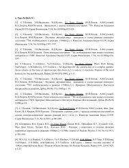
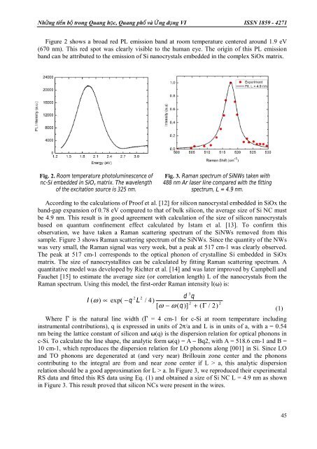
Nhữ<strong>ng</strong> tiến bộ <stro<strong>ng</strong>>tro<strong>ng</strong></stro<strong>ng</strong>> <stro<strong>ng</strong>>Qua<strong>ng</strong></stro<strong>ng</strong>> học, <stro<strong>ng</strong>>Qua<strong>ng</strong></stro<strong>ng</strong>> <stro<strong>ng</strong>>ph</stro<strong>ng</strong>>ổ và Ứ<strong>ng</strong> dụ<strong>ng</strong> <strong>VI</strong> <strong>ISSN</strong> <strong>1859</strong> - <strong>4271</strong>Figure 2 shows a broad red PL emission band at room temperature centered around 1.9 eV(670 nm). This red spot was clearly visible to the human eye. The origin of this PL emissionband can be attributed to the emission of Si nanocrystals embedded in the complex SiOx matrix.Fig. 2. Room temperature <stro<strong>ng</strong>>ph</stro<strong>ng</strong>>otoluminescence ofnc-Si embedded in SiO x matrix. The wavele<strong>ng</strong>thof the excitation source is 325 nm.Fig. 3. Raman spectrum of SiNWs taken with488 nm Ar laser line compared with the fit<s<stro<strong>ng</strong>>tro<strong>ng</strong></stro<strong>ng</strong>>>tin</s<stro<strong>ng</strong>>tro<strong>ng</strong></stro<strong>ng</strong>>>gspectrum, L = 4.9 nm.Accordi<strong>ng</strong> to the calculations of Proof et al. [12] for silicon nanocrystal embedded in SiOx theband-gap expansion of 0.78 eV compared to that of bulk silicon, the average size of Si NC mustbe 4.9 nm. This result is in good agreement with calculation of the size of silicon nanocrystalsbased on quantum confinement effect calculated by Istam et al. [13]. To confirm thisobservation, we have taken a Raman scatteri<strong>ng</strong> spectrum of the SiNWs removed from thissample. Figure 3 shows Raman scatteri<strong>ng</strong> spectrum of the SiNWs. Since the quantity of the NWswas very small, the Raman signal was very week, but a peak at 517 cm-1 was clearly observed.The peak at 517 cm-1 corresponds to the optical <stro<strong>ng</strong>>ph</stro<strong>ng</strong>>onon of crystalline Si embedded in SiOxmatrix. The size of nanocrystallites can be calculated by fit<s<stro<strong>ng</strong>>tro<strong>ng</strong></stro<strong>ng</strong>>>tin</s<stro<strong>ng</strong>>tro<strong>ng</strong></stro<strong>ng</strong>>>g Raman scatteri<strong>ng</strong> spectrum. Aquantitative model was developed by Richter et al. [14] and was later improved by Campbell andFauchet [15] to estimate the average size (or correlation le<strong>ng</strong>th) L of the nanocrystals from theRaman spectrum. Usi<strong>ng</strong> this model, the first-order Raman intensity I(ω) is:I ( ω ) ∝exp( −q2L23d q/ 4)2[ ω − ω ( q)]+ ( Γ / 2)Where Γ is the natural line width (Γ = 4 cm-1 for c-Si at room temperature includi<strong>ng</strong>instrumental contributions), q is expressed in units of 2π/a and L is in units of a, with a = 0.54nm bei<strong>ng</strong> the lattice constant of silicon and ω(q) is the dispersion relation for optical <stro<strong>ng</strong>>ph</stro<strong>ng</strong>>onons inc-Si. To calculate the line shape, the analytic form ω(q) = A – Bq2, with A = 518.6 cm-1 and B =10 cm-1, which reproduces the dispersion relation for LO <stro<strong>ng</strong>>ph</stro<strong>ng</strong>>onons alo<strong>ng</strong> [001] in Si. Since LOand TO <stro<strong>ng</strong>>ph</stro<strong>ng</strong>>onons are degenerated at (and very near) Brillouin zone center and the <stro<strong>ng</strong>>ph</stro<strong>ng</strong>>ononscontribu<s<stro<strong>ng</strong>>tro<strong>ng</strong></stro<strong>ng</strong>>>tin</s<stro<strong>ng</strong>>tro<strong>ng</strong></stro<strong>ng</strong>>>g to the integral are from and near zone center if L > a, this analytic dispersionrelation should be a good approximation for L > a. In Figure 3, we reproduced their experimentalRS data and fitted this RS data usi<strong>ng</strong> Eq. (1) and obtained a size of Si NC L = 4.9 nm as shownin Figure 3. This result proved that silicon NCs were present in the wires.2(1)45