1. Basic Concepts in Reliability Design - nl3prc
1. Basic Concepts in Reliability Design - nl3prc
1. Basic Concepts in Reliability Design - nl3prc

Create successful ePaper yourself
Turn your PDF publications into a flip-book with our unique Google optimized e-Paper software.
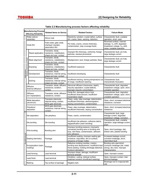
[2] <strong>Design</strong><strong>in</strong>g for <strong>Reliability</strong>Table 2.2 Manufactur<strong>in</strong>g process factors affect<strong>in</strong>g reliabilityManufactur<strong>in</strong>g ProcessRelated Items on Device Related Factors Failure ModeAffect<strong>in</strong>g <strong>Reliability</strong>Wafer processAssembly processWafer (siliconsubstrate)Oxide filmPhotoengrav<strong>in</strong>g process (PEP)Resist applicationMask alignmentExpos<strong>in</strong>gDevelopmentEtch<strong>in</strong>gDiffusion(thermal diffusion)Diffusion(ion implantation)Metal deposition(alum<strong>in</strong>um)PolysilicondepositionSilicon bulkField oxide, gate oxide,<strong>in</strong>terlayer <strong>in</strong>sulator,passivation filmTransistor, diode,resistance, metallization,shape and size, contactTransistor, diode,resistance, metallization,shape and size, contactTransistor, diode,resistance, metallization,shape and size, contactTransistor, diode,resistance, <strong>in</strong>ternal wir<strong>in</strong>g,shape and size, contactTransistor, diode,resistance, <strong>in</strong>ternal wir<strong>in</strong>g,shape and size, contactTransistor, diode, diffusionresistance, isolation,contactTransistor, diode, diffusionresistance, contactTransistor electrode,<strong>in</strong>ternal wir<strong>in</strong>g, contact,MOS gate electrodeMOS gate electrode,resistance, <strong>in</strong>ternal wir<strong>in</strong>g,contactResistivity variation, crystal defect, surfacedirt, cracks, flaws, warp<strong>in</strong>g, distortionP<strong>in</strong> holes, cracks, uneven thickness,contam<strong>in</strong>ation, step coverage faultsImproper film thickness, uniformity, foreignparticles, residual photoresistMisalignment, dust, foreign particles, flawsInsufficient exposureInsufficient develop<strong>in</strong>gInsufficient etch<strong>in</strong>g, etch<strong>in</strong>g temperature outof range, <strong>in</strong>sufficient wash<strong>in</strong>gAbnormal diffusion (transverse, depth),impurity separation, crystal defects,improper impurity concentrationOxide film, damaged silicon bulk,<strong>in</strong>sufficient dose amount, <strong>in</strong>sufficientimplantation depthFlaws, voids, step coverage, delam<strong>in</strong>ation,<strong>in</strong>sufficient thickness, electromigration,dop<strong>in</strong>g concentration, contam<strong>in</strong>ationFlaws, step coverage, delam<strong>in</strong>ation,<strong>in</strong>sufficient thickness, dop<strong>in</strong>g concentrationDie separation Die periphery Flaws, cracks, contam<strong>in</strong>ationDie bond<strong>in</strong>gWire bond<strong>in</strong>gSeal<strong>in</strong>g (hermetic)Encapsulation (res<strong>in</strong>mold<strong>in</strong>g)Lead form<strong>in</strong>gLead f<strong>in</strong>ishDie bond<strong>in</strong>gBond<strong>in</strong>g wirePackagePackageLead term<strong>in</strong>alLead term<strong>in</strong>alMark<strong>in</strong>g Top surface of package Illegible markInsufficient die adhesion, adhesive debris,degassification (res<strong>in</strong> bond<strong>in</strong>g)Improper bond<strong>in</strong>g pressure, improperlyconnected bond<strong>in</strong>g wire or bond<strong>in</strong>g wireloop, wire flaws, contam<strong>in</strong>ation, deficientwire adhesionInsufficient seal<strong>in</strong>g, improper seal<strong>in</strong>g gas(moisture, impurities), dirt on surface,presence of foreign matterCharacteristic fault, unstableoperation, short, openReversed surface, channelleakage, V th shift, degradedbreakdown voltage, h FE shift,noise, unstable operationCharacteristic fault, p<strong>in</strong> hole,large leakage currentCharacteristic fault, p<strong>in</strong> hole,large leakage currentCharacteristic faultCharacteristic faultCharacteristic fault,characteristic fluctuationCharacteristic fault, degradedbreakdown voltage, open, short,unstable operationCharacteristic fault, degradedbreakdown voltage, open, short,unstable operationOpen, short, <strong>in</strong>creased electricalresistance, corrosionOpen, short, <strong>in</strong>creased electricalresistanceCharacteristic fault, largeleakage current, degradedbreakdown voltage, corrosionCharacteristic fault, unstableoperation, large leakage current,shortOpen, short (package, die),broken wire, peeled bond<strong>in</strong>gIncreased leakage current,corrosion breakage, short,<strong>in</strong>termittent faultDefective mold<strong>in</strong>g (cavities, cracks), Bond<strong>in</strong>g wire open/short,bond<strong>in</strong>g wire displacement, <strong>in</strong>sufficient lead corrosion breakage (die, metalframe seal<strong>in</strong>g, mold<strong>in</strong>g shr<strong>in</strong>kage distortion, wir<strong>in</strong>g), die crack, impropermoisture absorptioncharacteristicsImproper shape, damage, <strong>in</strong>sufficientOpen, improper contactterm<strong>in</strong>al strengthOxidation, rust<strong>in</strong>g, residual surface Open, improper contact, <strong>in</strong>terterm<strong>in</strong>alleakagetreatment solution (<strong>in</strong>sufficient wash<strong>in</strong>g)Breakage due to <strong>in</strong>appropriateuse2-11