1. Basic Concepts in Reliability Design - nl3prc
1. Basic Concepts in Reliability Design - nl3prc
1. Basic Concepts in Reliability Design - nl3prc
You also want an ePaper? Increase the reach of your titles
YUMPU automatically turns print PDFs into web optimized ePapers that Google loves.
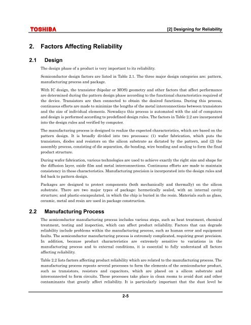
[2] <strong>Design</strong><strong>in</strong>g for <strong>Reliability</strong>2. Factors Affect<strong>in</strong>g <strong>Reliability</strong>2.1 <strong>Design</strong>The design phase of a product is very important to its reliability.Semiconductor design factors are listed <strong>in</strong> Table 2.<strong>1.</strong> The three major design categories are: pattern,manufactur<strong>in</strong>g process and package.With IC design, the transistor (bipolar or MOS) geometry and other factors that affect performanceare determ<strong>in</strong>ed dur<strong>in</strong>g the pattern design phase accord<strong>in</strong>g to the functional characteristics required ofthe device. Transistors are then connected to obta<strong>in</strong> the desired functions. Dur<strong>in</strong>g this process,cont<strong>in</strong>uous efforts are made to m<strong>in</strong>imize the lengths of the metal <strong>in</strong>terconnections between transistorsand the size of <strong>in</strong>dividual elements. Nowadays this process is automated with the aid of computersand design is performed accord<strong>in</strong>g to predef<strong>in</strong>ed design rules. The factors <strong>in</strong> Table 2.2 are <strong>in</strong>corporated<strong>in</strong>to the design rules and verified by computer.The manufactur<strong>in</strong>g process is designed to realize the expected characteristics, which are based on thepattern design. It is broadly divided <strong>in</strong>to two processes: (1) wafer fabrication, which puts thetransistors, diodes and resistors on the silicon substrate as dictated by the pattern, and (2) theassembly process, consist<strong>in</strong>g of die separation, die bond<strong>in</strong>g, wire bond<strong>in</strong>g and seal<strong>in</strong>g to form the f<strong>in</strong>alproduct structure.Dur<strong>in</strong>g wafer fabrication, various technologies are used to achieve exactly the right size and shape forthe diffusion layer, oxide film and metal <strong>in</strong>terconnections. Cont<strong>in</strong>uous efforts are made to ma<strong>in</strong>ta<strong>in</strong>consistency <strong>in</strong> these characteristics. Manufactur<strong>in</strong>g precision is <strong>in</strong>corporated <strong>in</strong>to the design rules andfed back to pattern design.Packages are designed to protect components (both mechanically and thermally) on the siliconsubstrate. There are two major types of package: hermetically sealed, with an <strong>in</strong>ternal cavitystructure; and plastic-encapsulated, <strong>in</strong> which the chip is buried <strong>in</strong> the res<strong>in</strong>. Materials such as glass,ceramic, metal and res<strong>in</strong> are used <strong>in</strong> package construction.2.2 Manufactur<strong>in</strong>g ProcessThe semiconductor manufactur<strong>in</strong>g process <strong>in</strong>cludes various steps, such as heat treatment, chemicaltreatment, test<strong>in</strong>g and <strong>in</strong>spection, which can affect product reliability. Factors that can degradereliability <strong>in</strong>clude problems with<strong>in</strong> the manufactur<strong>in</strong>g process, such as human error and equipmentfaults. The semiconductor manufactur<strong>in</strong>g process is extremely complicated, requir<strong>in</strong>g great precision.In addition, because product characteristics are extremely sensitive to variations <strong>in</strong> themanufactur<strong>in</strong>g process and to external conditions, it is essential to fully understand all factorsaffect<strong>in</strong>g reliability.Table 2.2 lists factors affect<strong>in</strong>g product reliability which are related to the manufactur<strong>in</strong>g process. Themanufactur<strong>in</strong>g process repeats several processes to form the elements of the semiconductor product,such as transistors, resistors and capacitors, which are placed on a silicon substrate and<strong>in</strong>terconnected to form circuits. These processes take place <strong>in</strong> clean rooms to avoid dust and othercontam<strong>in</strong>ants that greatly affect reliability. It is particularly important that the dust level be2-5


