1. Basic Concepts in Reliability Design - nl3prc
1. Basic Concepts in Reliability Design - nl3prc
1. Basic Concepts in Reliability Design - nl3prc

Create successful ePaper yourself
Turn your PDF publications into a flip-book with our unique Google optimized e-Paper software.
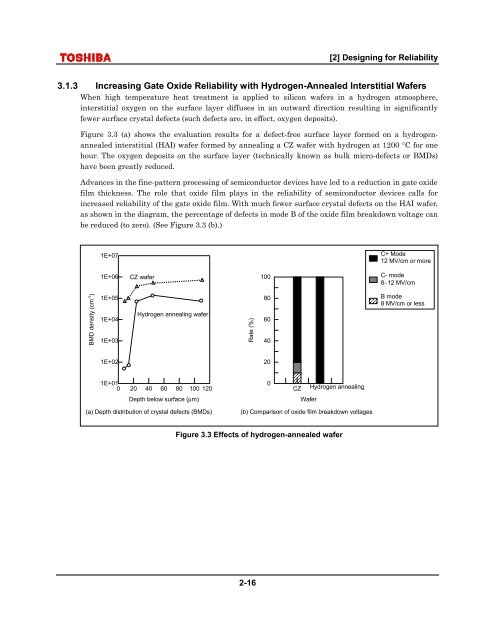
[2] <strong>Design</strong><strong>in</strong>g for <strong>Reliability</strong>3.<strong>1.</strong>3 Increas<strong>in</strong>g Gate Oxide <strong>Reliability</strong> with Hydrogen-Annealed Interstitial WafersWhen high temperature heat treatment is applied to silicon wafers <strong>in</strong> a hydrogen atmosphere,<strong>in</strong>terstitial oxygen on the surface layer diffuses <strong>in</strong> an outward direction result<strong>in</strong>g <strong>in</strong> significantlyfewer surface crystal defects (such defects are, <strong>in</strong> effect, oxygen deposits).Figure 3.3 (a) shows the evaluation results for a defect-free surface layer formed on a hydrogenannealed<strong>in</strong>terstitial (HAI) wafer formed by anneal<strong>in</strong>g a CZ wafer with hydrogen at 1200 °C for onehour. The oxygen deposits on the surface layer (technically known as bulk micro-defects or BMDs)have been greatly reduced.Advances <strong>in</strong> the f<strong>in</strong>e-pattern process<strong>in</strong>g of semiconductor devices have led to a reduction <strong>in</strong> gate oxidefilm thickness. The role that oxide film plays <strong>in</strong> the reliability of semiconductor devices calls for<strong>in</strong>creased reliability of the gate oxide film. With much fewer surface crystal defects on the HAI wafer,as shown <strong>in</strong> the diagram, the percentage of defects <strong>in</strong> mode B of the oxide film breakdown voltage canbe reduced (to zero). (See Figure 3.3 (b).)1E+07C+ Mode12 MV/cm or more1E+06CZ wafer100C- mode8∼12 MV/cmBMD density (cm -2 )1E+051E+041E+03Hydrogen anneal<strong>in</strong>g waferRate (%)806040B mode8 MV/cm or less1E+02201E+010 20 40 60 80 100 120Depth below surface (µm)0CZ Hydrogen anneal<strong>in</strong>gWafer(a) Depth distribution of crystal defects (BMDs)(b) Comparison of oxide film breakdown voltagesFigure 3.3 Effects of hydrogen-annealed wafer2-16