1. Basic Concepts in Reliability Design - nl3prc
1. Basic Concepts in Reliability Design - nl3prc
1. Basic Concepts in Reliability Design - nl3prc

Create successful ePaper yourself
Turn your PDF publications into a flip-book with our unique Google optimized e-Paper software.
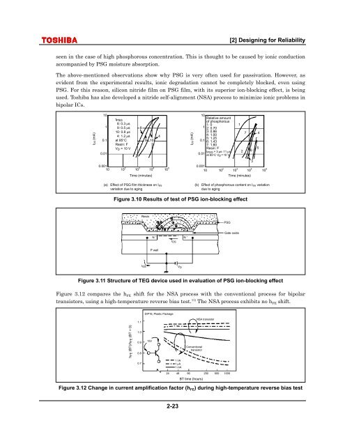
[2] <strong>Design</strong><strong>in</strong>g for <strong>Reliability</strong>seen <strong>in</strong> the case of high phosphorous concentration. This is thought to be caused by ionic conductionaccompanied by PSG moisture absorption.The above-mentioned observations show why PSG is very often used for passivation. However, asevident from the experimental results, ionic degradation cannot be completely blocked, even us<strong>in</strong>gPSG. For this reason, silicon nitride film on PSG film, with its superior ion-block<strong>in</strong>g effect, is be<strong>in</strong>gused. Toshiba has also developed a nitride self-alignment (NSA) process to m<strong>in</strong>imize ionic problems <strong>in</strong>bipolar ICs.IDS (mA)1010.10.01t PSG8: 0.3 µs9: 0.5 µs10: 0.8 µs4: <strong>1.</strong>2 µsat 85°CRes<strong>in</strong>: FV D = 10 V89104IDS (mA)1010.10.01Relative amountof phosphorous1: 02: 0.703: 0.864: <strong>1.</strong>005: <strong>1.</strong>256: <strong>1.</strong>437: <strong>1.</strong>60Res<strong>in</strong>: Ft PSG = 3 µs∼11 µsat 85°C V D = 10 V1276450.0011010 210 3Time (m<strong>in</strong>utes)10 50.0011010 210 4 (b) Effect of phosphorous content on I DS variation10 310 4Time (m<strong>in</strong>utes)310 5(a)Effect of PSG film thickness on I DSvariation due to ag<strong>in</strong>gdue to ag<strong>in</strong>gFigure 3.10 Results of test of PSG ion-block<strong>in</strong>g effectRes<strong>in</strong>PSGN +I DSN +Gate oxideP wellI DSV DFigure 3.11 Structure of TEG device used <strong>in</strong> evaluation of PSG ion-block<strong>in</strong>g effectFigure 3.12 compares the h FE shift for the NSA process with the conventional process for bipolartransistors, us<strong>in</strong>g a high-temperature reverse bias test. 11) The NSA process exhibits no h FE shift.DIP16, Plastic Package<strong>1.</strong>1NSA transistorhFE (BT)/hFE (BT = 0)<strong>1.</strong>00.90.80.715V1 nA1 µA1 mAConventionaltransistor24 48 96250 500 1000BT time (hours)Figure 3.12 Change <strong>in</strong> current amplification factor (h FE ) dur<strong>in</strong>g high-temperature reverse bias test2-23