1. Basic Concepts in Reliability Design - nl3prc
1. Basic Concepts in Reliability Design - nl3prc
1. Basic Concepts in Reliability Design - nl3prc

Create successful ePaper yourself
Turn your PDF publications into a flip-book with our unique Google optimized e-Paper software.
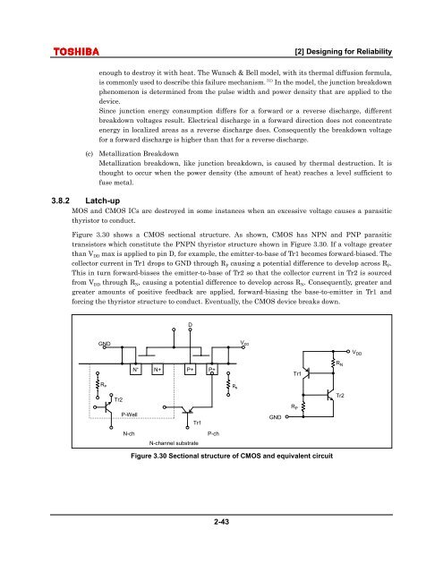
[2] <strong>Design</strong><strong>in</strong>g for <strong>Reliability</strong>enough to destroy it with heat. The Wunsch & Bell model, with its thermal diffusion formula,is commonly used to describe this failure mechanism. 31) In the model, the junction breakdownphenomenon is determ<strong>in</strong>ed from the pulse width and power density that are applied to thedevice.S<strong>in</strong>ce junction energy consumption differs for a forward or a reverse discharge, differentbreakdown voltages result. Electrical discharge <strong>in</strong> a forward direction does not concentrateenergy <strong>in</strong> localized areas as a reverse discharge does. Consequently the breakdown voltagefor a forward discharge is higher than that for a reverse discharge.(c) Metallization BreakdownMetallization breakdown, like junction breakdown, is caused by thermal destruction. It isthought to occur when the power density (the amount of heat) reaches a level sufficient tofuse metal.3.8.2 Latch-upMOS and CMOS ICs are destroyed <strong>in</strong> some <strong>in</strong>stances when an excessive voltage causes a parasiticthyristor to conduct.Figure 3.30 shows a CMOS sectional structure. As shown, CMOS has NPN and PNP parasitictransistors which constitute the PNPN thyristor structure shown <strong>in</strong> Figure 3.30. If a voltage greaterthan V DD max is applied to p<strong>in</strong> D, for example, the emitter-to-base of Tr1 becomes forward-biased. Thecollector current <strong>in</strong> Tr1 drops to GND through R P caus<strong>in</strong>g a potential difference to develop across R P .This <strong>in</strong> turn forward-biases the emitter-to-base of Tr2 so that the collector current <strong>in</strong> Tr2 is sourcedfrom V DD through R N , caus<strong>in</strong>g a potential difference to develop across R N . Consequently, greater andgreater amounts of positive feedback are applied, forward-bias<strong>in</strong>g the base-to-emitter <strong>in</strong> Tr1 andforc<strong>in</strong>g the thyristor structure to conduct. Eventually, the CMOS device breaks down.DGNDV DDV DDN + N+P+ P+Tr1R NR PR NTr2Tr2P-WellTr1GNDR PN-chP-chN-channel substrateFigure 3.30 Sectional structure of CMOS and equivalent circuit2-43