1. Basic Concepts in Reliability Design - nl3prc
1. Basic Concepts in Reliability Design - nl3prc
1. Basic Concepts in Reliability Design - nl3prc

Create successful ePaper yourself
Turn your PDF publications into a flip-book with our unique Google optimized e-Paper software.
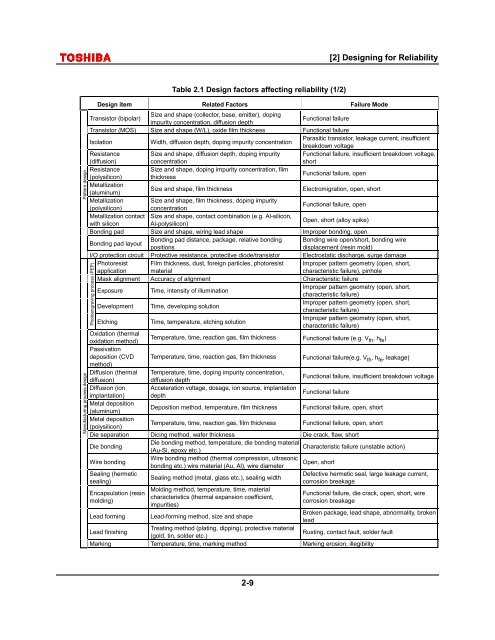
[2] <strong>Design</strong><strong>in</strong>g for <strong>Reliability</strong>Pattern designManufactur<strong>in</strong>g process designPhotoengrav<strong>in</strong>g process (PEP)Table 2.1 <strong>Design</strong> factors affect<strong>in</strong>g reliability (1/2)<strong>Design</strong> item Related Factors Failure ModeTransistor (bipolar)Size and shape (collector, base, emitter), dop<strong>in</strong>gimpurity concentration, diffusion depthFunctional failureTransistor (MOS) Size and shape (W/L), oxide film thickness Functional failureIsolationWidth, diffusion depth, dop<strong>in</strong>g impurity concentrationParasitic transistor, leakage current, <strong>in</strong>sufficientbreakdown voltageResistance(diffusion)Size and shape, diffusion depth, dop<strong>in</strong>g impurityconcentrationFunctional failure, <strong>in</strong>sufficient breakdown voltage,shortResistanceSize and shape, dop<strong>in</strong>g impurity concentration, film(polysilicon) thicknessFunctional failure, openMetallization(alum<strong>in</strong>um)Size and shape, film thicknessElectromigration, open, shortMetallization Size and shape, film thickness, dop<strong>in</strong>g impurity(polysilicon) concentrationFunctional failure, openMetallization contact Size and shape, contact comb<strong>in</strong>ation (e.g. Al-silicon,with siliconAl-polysilicon)Open, short (alloy spike)Bond<strong>in</strong>g pad Size and shape, wir<strong>in</strong>g lead shape Improper bond<strong>in</strong>g, openBond<strong>in</strong>g pad layoutBond<strong>in</strong>g pad distance, package, relative bond<strong>in</strong>g Bond<strong>in</strong>g wire open/short, bond<strong>in</strong>g wirepositionsdisplacement (res<strong>in</strong> mold)I/O protection circuit Protective resistance, protective diode/transistor Electrostatic discharge, surge damagePhotoresist Film thickness, dust, foreign particles, photoresist Improper pattern geometry (open, short,application materialcharacteristic failure), p<strong>in</strong>holeMask alignment Accuracy of alignment Characteristic failureExposure Time, <strong>in</strong>tensity of illum<strong>in</strong>ationImproper pattern geometry (open, short,characteristic failure)Development Time, develop<strong>in</strong>g solutionImproper pattern geometry (open, short,characteristic failure)Etch<strong>in</strong>gTime, temperature, etch<strong>in</strong>g solutionImproper pattern geometry (open, short,characteristic failure)Oxidation (thermaloxidation method)Temperature, time, reaction gas, film thickness Functional failure (e.g. V th , h fe )Passivationdeposition (CVD Temperature, time, reaction gas, film thickness Functional failure(e.g. V th , h fe , leakage)method)Diffusion (thermal Temperature, time, dop<strong>in</strong>g impurity concentration,diffusion)diffusion depthFunctional failure, <strong>in</strong>sufficient breakdown voltageDiffusion (ion Acceleration voltage, dosage, ion source, implantationimplantation) depthFunctional failureMetal deposition(alum<strong>in</strong>um)Deposition method, temperature, film thickness Functional failure, open, shortMetal deposition(polysilicon)Temperature, time, reaction gas, film thickness Functional failure, open, shortDie separation Dic<strong>in</strong>g method, wafer thickness Die crack, flaw, shortDie bond<strong>in</strong>gDie bond<strong>in</strong>g method, temperature, die bond<strong>in</strong>g material(Au-Si, epoxy etc.)Characteristic failure (unstable action)Wire bond<strong>in</strong>gWire bond<strong>in</strong>g method (thermal compression, ultrasonicbond<strong>in</strong>g etc.) wire material (Au, Al), wire diameterOpen, shortSeal<strong>in</strong>g (hermeticDefective hermetic seal, large leakage current,Seal<strong>in</strong>g method (metal, glass etc.), seal<strong>in</strong>g widthseal<strong>in</strong>g)corrosion breakageEncapsulation (res<strong>in</strong>mold<strong>in</strong>g)Mold<strong>in</strong>g method, temperature, time, materialcharacteristics (thermal expansion coefficient,impurities)Functional failure, die crack, open, short, wirecorrosion breakageLead form<strong>in</strong>g Lead-form<strong>in</strong>g method, size and shapeBroken package, lead shape, abnormality, brokenleadLead f<strong>in</strong>ish<strong>in</strong>gTreat<strong>in</strong>g method (plat<strong>in</strong>g, dipp<strong>in</strong>g), protective material(gold, t<strong>in</strong>, solder etc.)Rust<strong>in</strong>g, contact fault, solder faultMark<strong>in</strong>g Temperature, time, mark<strong>in</strong>g method Mark<strong>in</strong>g erosion, illegibility2-9