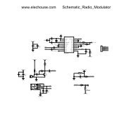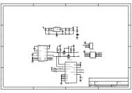
Clike here to get datasheet of CC1101 - Elechouse
Clike here to get datasheet of CC1101 - Elechouse
Clike here to get datasheet of CC1101 - Elechouse

You also want an ePaper? Increase the reach of your titles
YUMPU automatically turns print PDFs into web optimized ePapers that Google loves.
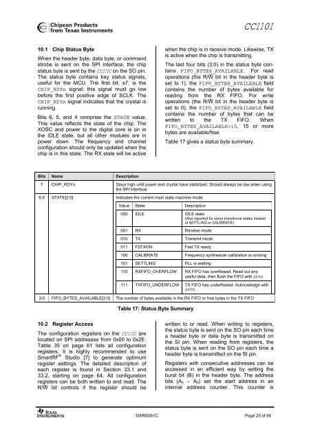
<strong>CC1101</strong>10.1 Chip Status ByteWhen the header byte, data byte, or commandstrobe is sent on the SPI interface, the chipstatus byte is sent by the <strong>CC1101</strong> on the SO pin.The status byte contains key status signals,useful for the MCU. The first bit, s7, is theCHIP_RDYn signal; this signal must go lowbefore the first positive edge <strong>of</strong> SCLK. TheCHIP_RDYn signal indicates that the crystal isrunning.Bits 6, 5, and 4 comprise the STATE value.This value reflects the state <strong>of</strong> the chip. TheXOSC and power <strong>to</strong> the digital core is on inthe IDLE state, but all other modules are inpower down. The frequency and channelconfiguration should only be updated when thechip is in this state. The RX state will be activewhen the chip is in receive mode. Likewise, TXis active when the chip is transmitting.The last four bits (3:0) in the status byte containsFIFO_BYTES_AVAILABLE. For readoperations (the R/W¯ bit in the header byte isset <strong>to</strong> 1), the FIFO_BYTES_AVAILABLE fieldcontains the number <strong>of</strong> bytes available forreading from the RX FIFO. For writeoperations (the R/W¯ bit in the header byte isset <strong>to</strong> 0), the FIFO_BYTES_AVAILABLE fieldcontains the number <strong>of</strong> bytes that can bewritten <strong>to</strong> the TX FIFO. WhenFIFO_BYTES_AVAILABLE=15, 15 or morebytes are available/free.Table 17 gives a status byte summary.Bits Name Description7 CHIP_RDYn Stays high until power and crystal have stabilized. Should always be low when usingthe SPI interface.6:4 STATE[2:0] Indicates the current main state machine modeValue State Description000 IDLE IDLE state(Also reported for some transitional states instead<strong>of</strong> SETTLING or CALIBRATE)001 RX Receive mode010 TX Transmit mode011 FSTXON Fast TX ready100 CALIBRATE Frequency synthesizer calibration is running101 SETTLING PLL is settling110 RXFIFO_OVERFLOW RX FIFO has overflowed. Read out anyuseful data, then flush the FIFO with SFRX111 TXFIFO_UNDERFLOW TX FIFO has underflowed. Acknowledge withSFTX3:0 FIFO_BYTES_AVAILABLE[3:0] The number <strong>of</strong> bytes available in the RX FIFO or free bytes in the TX FIFOTable 17: Status Byte Summary10.2 Register AccessThe configuration registers on the <strong>CC1101</strong> arelocated on SPI addresses from 0x00 <strong>to</strong> 0x2E.Table 35 on page 61 lists all configurationregisters. It is highly recommended <strong>to</strong> useSmartRF ® Studio [7] <strong>to</strong> generate optimumregister settings. The detailed description <strong>of</strong>each register is found in Section 33.1 and33.2, starting on page 64. All configurationregisters can be both written <strong>to</strong> and read. TheR/W¯ bit controls if the register should bewritten <strong>to</strong> or read. When writing <strong>to</strong> registers,the status byte is sent on the SO pin each timea header byte or data byte is transmitted onthe SI pin. When reading from registers, thestatus byte is sent on the SO pin each time aheader byte is transmitted on the SI pin.Registers with consecutive addresses can beaccessed in an efficient way by setting theburst bit (B) in the header byte. The addressbits (A 5 – A 0 ) set the start address in aninternal address counter. This counter isSWRS061C Page 25 <strong>of</strong> 94