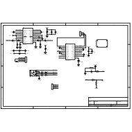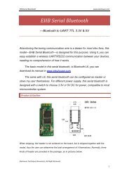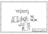
Clike here to get datasheet of CC1101 - Elechouse
Clike here to get datasheet of CC1101 - Elechouse
Clike here to get datasheet of CC1101 - Elechouse

Create successful ePaper yourself
Turn your PDF publications into a flip-book with our unique Google optimized e-Paper software.
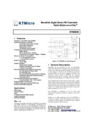
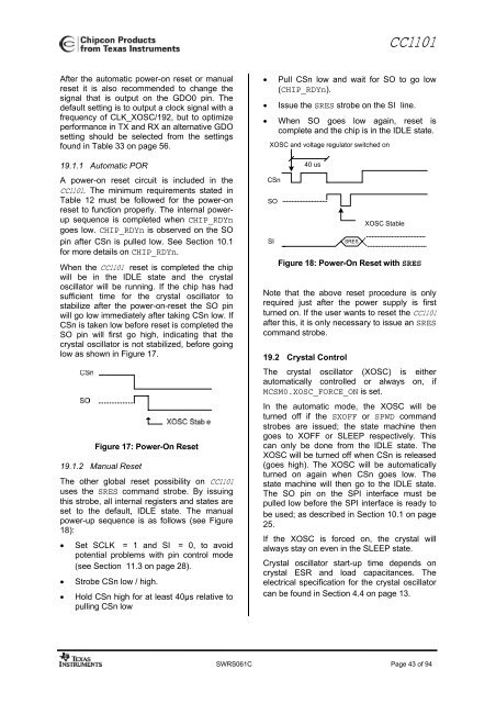
<strong>CC1101</strong>After the au<strong>to</strong>matic power-on reset or manualreset it is also recommended <strong>to</strong> change thesignal that is output on the GDO0 pin. Thedefault setting is <strong>to</strong> output a clock signal with afrequency <strong>of</strong> CLK_XOSC/192, but <strong>to</strong> optimizeperformance in TX and RX an alternative GDOsetting should be selected from the settingsfound in Table 33 on page 56.19.1.1 Au<strong>to</strong>matic PORA power-on reset circuit is included in the<strong>CC1101</strong>. The minimum requirements stated inTable 12 must be followed for the power-onreset <strong>to</strong> function properly. The internal powerupsequence is completed when CHIP_RDYngoes low. CHIP_RDYn is observed on the SOpin after CSn is pulled low. See Section 10.1for more details on CHIP_RDYn.When the <strong>CC1101</strong> reset is completed the chipwill be in the IDLE state and the crystaloscilla<strong>to</strong>r will be running. If the chip has hadsufficient time for the crystal oscilla<strong>to</strong>r <strong>to</strong>stabilize after the power-on-reset the SO pinwill go low immediately after taking CSn low. IfCSn is taken low before reset is completed theSO pin will first go high, indicating that thecrystal oscilla<strong>to</strong>r is not stabilized, before goinglow as shown in Figure 17.Figure 17: Power-On Reset19.1.2 Manual ResetThe other global reset possibility on <strong>CC1101</strong>uses the SRES command strobe. By issuingthis strobe, all internal registers and states areset <strong>to</strong> the default, IDLE state. The manualpower-up sequence is as follows (see Figure18):• Set SCLK = 1 and SI = 0, <strong>to</strong> avoidpotential problems with pin control mode(see Section 11.3 on page 28).• Strobe CSn low / high.• Hold CSn high for at least 40µs relative <strong>to</strong>pulling CSn low• Pull CSn low and wait for SO <strong>to</strong> go low(CHIP_RDYn).• Issue the SRES strobe on the SI line.• When SO goes low again, reset iscomplete and the chip is in the IDLE state.XOSC and voltage regula<strong>to</strong>r switched onCSnSOSI40 usSRESXOSC StableFigure 18: Power-On Reset with SRESNote that the above reset procedure is onlyrequired just after the power supply is firstturned on. If the user wants <strong>to</strong> reset the <strong>CC1101</strong>after this, it is only necessary <strong>to</strong> issue an SREScommand strobe.19.2 Crystal ControlThe crystal oscilla<strong>to</strong>r (XOSC) is eitherau<strong>to</strong>matically controlled or always on, ifMCSM0.XOSC_FORCE_ON is set.In the au<strong>to</strong>matic mode, the XOSC will beturned <strong>of</strong>f if the SXOFF or SPWD commandstrobes are issued; the state machine thengoes <strong>to</strong> XOFF or SLEEP respectively. Thiscan only be done from the IDLE state. TheXOSC will be turned <strong>of</strong>f when CSn is released(goes high). The XOSC will be au<strong>to</strong>maticallyturned on again when CSn goes low. Thestate machine will then go <strong>to</strong> the IDLE state.The SO pin on the SPI interface must bepulled low before the SPI interface is ready <strong>to</strong>be used; as described in Section 10.1 on page25.If the XOSC is forced on, the crystal willalways stay on even in the SLEEP state.Crystal oscilla<strong>to</strong>r start-up time depends oncrystal ESR and load capacitances. Theelectrical specification for the crystal oscilla<strong>to</strong>rcan be found in Section 4.4 on page 13.SWRS061C Page 43 <strong>of</strong> 94