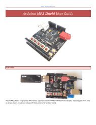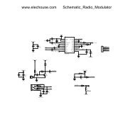
Clike here to get datasheet of CC1101 - Elechouse
Clike here to get datasheet of CC1101 - Elechouse
Clike here to get datasheet of CC1101 - Elechouse

You also want an ePaper? Increase the reach of your titles
YUMPU automatically turns print PDFs into web optimized ePapers that Google loves.
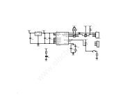
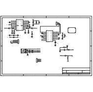
<strong>CC1101</strong>23 Voltage Regula<strong>to</strong>rs<strong>CC1101</strong> contains several on-chip linear voltageregula<strong>to</strong>rs, which generate the supply voltageneeded by low-voltage modules. Thesevoltage regula<strong>to</strong>rs are invisible <strong>to</strong> the user, andcan be viewed as integral parts <strong>of</strong> the variousmodules. The user must however make surethat the absolute maximum ratings andrequired pin voltages in Table 1 and Table 13are not exceeded. The voltage regula<strong>to</strong>r forthe digital core requires one externaldecoupling capaci<strong>to</strong>r.24 Output Power ProgrammingThe RF output power level from the devicehas two levels <strong>of</strong> programmability, asillustrated in Figure 22. Firstly, the specialPATABLE register can hold up <strong>to</strong> eight userselected output power settings. Secondly, the3-bit FREND0.PA_POWER value selects thePATABLE entry <strong>to</strong> use. This two-levelfunctionality provides flexible PA power rampup and ramp down at the start and end <strong>of</strong>transmission, as well as ASK modulationshaping. All the PA power settings in thePATABLE from index 0 up <strong>to</strong> theFREND0.PA_POWER value are used.The power ramping at the start and at the end<strong>of</strong> a packet can be turned <strong>of</strong>f by settingFREND0.PA_POWER <strong>to</strong> zero and thenprogram the desired output power <strong>to</strong> index 0 inthe PATABLE.Setting the CSn pin low turns on the voltageregula<strong>to</strong>r <strong>to</strong> the digital core and starts thecrystal oscilla<strong>to</strong>r. The SO pin on the SPIinterface must go low before the first positiveedge <strong>of</strong> SCLK. (setup time is given in Table16).If the chip is programmed <strong>to</strong> enter power-downmode, (SPWD strobe issued), the power will beturned <strong>of</strong>f after CSn goes high. The power andcrystal oscilla<strong>to</strong>r will be turned on again whenCSn goes low.The voltage regula<strong>to</strong>r output should only beused for driving the <strong>CC1101</strong>.If OOK modulation is used, the logic 0 andlogic 1 power levels shall be programmed <strong>to</strong>index 0 and 1 respectively.Table 30 contains recommended PATABLEsettings for various output levels andfrequency bands. Using PA settings from 0x61<strong>to</strong> 0x6F is not recommended. See Section10.6 on page 27 for PATABLE programmingdetails.Table 31 contains output power and currentconsumption for default PATABLE setting(0xC6). PATABLE must be programmed inburst mode if you want <strong>to</strong> write <strong>to</strong> other entriesthan PATABLE[0].Note that all content <strong>of</strong> the PATABLE, exceptfor the first byte (index 0) is lost when enteringthe SLEEP state.SWRS061C Page 49 <strong>of</strong> 94