<strong>CC1101</strong>incremented by one each new byte (every 8clock pulses). The burst access is either aread or a write access and must be terminatedby setting CSn high.For register addresses in the range 0x30-0x3D, the burst bit is used <strong>to</strong> select betweenstatus registers, burst bit is one, and commandstrobes, burst bit is zero (see 10.4 below).Because <strong>of</strong> this, burst access is not availablefor status registers and they must be accessesone at a time. The status registers can only beread.10.3 SPI ReadWhen reading register fields over the SPIinterface while the register fields are updatedby the radio hardware (e.g. MARCSTATE orTXBYTES), t<strong>here</strong> is a small, but finite,probability that a single read from the registeris being corrupt. As an example, theprobability <strong>of</strong> any single read from TXBYTESbeing corrupt, assuming the maximum datarate is used, is approximately 80 ppm. Refer <strong>to</strong>the <strong>CC1101</strong> Errata Notes [1] for more details.10.4 Command StrobesCommand Strobes may be viewed as singlebyte instructions <strong>to</strong> <strong>CC1101</strong>. By addressing acommand strobe register, internal sequenceswill be started. These commands are used <strong>to</strong>disable the crystal oscilla<strong>to</strong>r, enable receivemode, enable wake-on-radio etc. The 13command strobes are listed in Table 34 onpage 60.The command strobe registers are accessedby transferring a single header byte (no data isbeing transferred). That is, only the R/W¯ bit,the burst access bit (set <strong>to</strong> 0), and the sixaddress bits (in the range 0x30 through 0x3D)are written. The R/W¯ bit can be either one orzero and will determine how theFIFO_BYTES_AVAILABLE field in the statusbyte should be interpreted.When writing command strobes, the statusbyte is sent on the SO pin.A command strobe may be followed by anyother SPI access without pulling CSn high.However, if an SRES strobe is being issued,one will have <strong>to</strong> waith for SO <strong>to</strong> go low againbefore the next header byte can be issued asshown in Figure 8. The command strobes areexecuted immediately, with the exception <strong>of</strong>the SPWD and the SXOFF strobes that areexecuted when CSn goes high.Figure 8: SRES Command Strobe10.5 FIFO AccessThe 64-byte TX FIFO and the 64-byte RXFIFO are accessed through the 0x3F address.When the R/W¯ bit is zero, the TX FIFO isaccessed, and the RX FIFO is accessed whenthe R/W¯ bit is one.The TX FIFO is write-only, while the RX FIFOis read-only.The burst bit is used <strong>to</strong> determine if the FIFOaccess is a single byte access or a burstaccess. The single byte access methodexpects a header byte with the burst bit set <strong>to</strong>zero and one data byte. After the data byte anew header byte is expected; hence, CSn canremain low. The burst access method expectsone header byte and then consecutive databytes until terminating the access by settingCSn high.The following header bytes access the FIFOs:• 0x3F: Single byte access <strong>to</strong> TX FIFO• 0x7F: Burst access <strong>to</strong> TX FIFO• 0xBF: Single byte access <strong>to</strong> RX FIFO• 0xFF: Burst access <strong>to</strong> RX FIFOWhen writing <strong>to</strong> the TX FIFO, the status byte(see Section 10.1) is output for each new databyte on SO, as shown in Figure 7. This statusbyte can be used <strong>to</strong> detect TX FIFO underflowwhile writing data <strong>to</strong> the TX FIFO. Note thatthe status byte contains the number <strong>of</strong> bytesfree before writing the byte in progress <strong>to</strong> theTX FIFO. When the last byte that fits in the TXFIFO is transmitted on SI, the status bytereceived concurrently on SO will indicate tha<strong>to</strong>ne byte is free in the TX FIFO.The TX FIFO may be flushed by issuing aSFTX command strobe. Similarly, a SFRXcommand strobe will flush the RX FIFO. ASFTX or SFRX command strobe can only beissued in the IDLE, TXFIFO_UNDERLOW, orRXFIFO_OVERFLOW states. Both FIFOs areflushed when going <strong>to</strong> the SLEEP state.SWRS061C Page 26 <strong>of</strong> 94
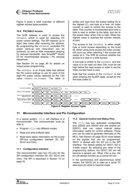
<strong>CC1101</strong>Figure 9 gives a brief overview <strong>of</strong> differentregister access types possible.10.6 PATABLE AccessThe 0x3E address is used <strong>to</strong> access thePATABLE, which is used for selecting PApower control settings. The SPI expects up <strong>to</strong>eight data bytes after receiving the address.By programming the PATABLE, controlled PApower ramp-up and ramp-down can beachieved, as well as ASK modulation shapingfor reduced bandwidth. See SmartRF ® Studio[7] for recommended shaping / PA rampingsequences.See Section 24 on page 49 for details onoutput power programming.The PATABLE is an 8-byte table that definesthe PA control settings <strong>to</strong> use for each <strong>of</strong> theeight PA power values (selected by the 3-bitvalue FREND0.PA_POWER). The table iswritten and read from the lowest setting (0) <strong>to</strong>the highest (7), one byte at a time. An indexcounter is used <strong>to</strong> control the access <strong>to</strong> thetable. This counter is incremented each time abyte is read or written <strong>to</strong> the table, and set <strong>to</strong>the lowest index when CSn is high. When thehighest value is reached the counter restartsat zero.The access <strong>to</strong> the PATABLE is either singlebyte or burst access depending on the burstbit. When using burst access the index counterwill count up; when reaching 7 the counter willrestart at 0. The R/W¯ bit controls whether theaccess is a read or a write access.If one byte is written <strong>to</strong> the PATABLE and thisvalue is <strong>to</strong> be read out then CSn must be sethigh before the read access in order <strong>to</strong> set theindex counter back <strong>to</strong> zero.Note that the content <strong>of</strong> the PATABLE is lostwhen entering the SLEEP state, except for thefirst byte (index 0).Figure 9: Register Access Types11 Microcontroller Interface and Pin ConfigurationIn a typical system, <strong>CC1101</strong> will interface <strong>to</strong> amicrocontroller. This microcontroller must beable <strong>to</strong>:• Program <strong>CC1101</strong> in<strong>to</strong> different modes• Read and write buffered data• Read back status information via the 4-wireSPI-bus configuration interface (SI, SO,SCLK and CSn).11.1 Configuration InterfaceThe microcontroller uses four I/O pins for theSPI configuration interface (SI, SO, SCLK andCSn). The SPI is described in Section 10 onpage 23.11.2 General Control and Status PinsThe <strong>CC1101</strong> has two dedicated configurablepins (GDO0 and GDO2) and one shared pin(GDO1) that can output internal statusinformation useful for control s<strong>of</strong>tware. Thesepins can be used <strong>to</strong> generate interrupts on theMCU. See Section 30 page 55 for more detailson the signals that can be programmed.GDO1 is shared with the SO pin in the SPIinterface. The default setting for GDO1/SO is3-state output. By selecting any other <strong>of</strong> theprogramming options, the GDO1/SO pin willbecome a generic pin. When CSn is low, thepin will always function as a normal SO pin.In the synchronous and asynchronous serialmodes, the GDO0 pin is used as a serial TXdata input pin while in transmit mode.SWRS061C Page 27 <strong>of</strong> 94