PHYSIOLOGICAL-READOUT
ISSCC2017AdvanceProgram
ISSCC2017AdvanceProgram

Create successful ePaper yourself
Turn your PDF publications into a flip-book with our unique Google optimized e-Paper software.
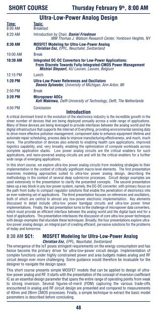
SHORT COURSE<br />
Thursday February 9 th , 8:00 AM<br />
Ultra-Low-Power Analog Design<br />
Time: Topic:<br />
8:00 AM Breakfast<br />
8:20 AM Introduction by Chair, Daniel Friedman<br />
IBM Thomas J. Watson Research Center, Yorktown Heights, NY<br />
8:30 AM MOSFET Modeling for Ultra-Low-Power Analog<br />
Christian Enz, EPFL, Neuchatel, Switzerland<br />
10:00 AM Break<br />
10:30 AM Integrated DC-DC Converters for Low-Power Applications:<br />
From Discrete Towards Fully-Integrated-CMOS Power Management<br />
Michiel Steyaert, KU Leuven, Leuven, Belgium<br />
12:15 PM Lunch<br />
1:20 PM Ultra-Low-Power References and Oscillators<br />
Dennis Sylvester, University of Michigan, Ann Arbor, MI<br />
2:50 PM Break<br />
3:20 PM Micropower ADCs<br />
Kofi Makinwa, Delft University of Technology, Delft, The Netherlands<br />
4:50 PM Conclusion<br />
Introduction<br />
A critical dominant trend in the evolution of the electronics industry is the incredible growth in the<br />
sheer number of devices that are being deployed annually across a wide range of applications.<br />
Many of these devices are being leveraged to provide interfaces between the analog world and the<br />
digital infrastructure that supports the Internet of Everything, providing environmental sensing data<br />
to drive more effective pollution management, component data to enhance equipment lifetime and<br />
automate repair scheduling, process data to improve manufacturing effectiveness, and much, much<br />
more. The proliferation of devices also extends to enabling health care applications, improved<br />
logistics capability, and, very broadly, enabling the optimization of compute workloads across<br />
complete application stacks. Low power analog circuits are the critical enablers for such<br />
applications, and nano-powered analog circuits are and will be the critical enablers for a further<br />
wide range of emerging applications.<br />
In this short course, we explore ultra-low power analog circuits from modeling strategies to their<br />
implementation in the context of critically significant macro-level elements. The first presentation<br />
examines modeling approaches suited to ultra-low power analog design, describing the<br />
methodology in the context of several deep submicron processes. Circuit design examples are<br />
used extensively in the presentation to clarify the presented concepts. The second presentation<br />
takes up a key block in any low power system, namely, the DC-DC converter, with primary focus on<br />
the path from bulky to compact regulator solutions that enable the penetration of electronics into<br />
an ever-widening set of applications. The third presentation focuses on references and oscillators,<br />
both of which are central to almost any low-power electronic implementation. Key elements<br />
discussed in detail include ultra-low power bandgap circuits and ultra-low power timer<br />
implementations. Finally, the last presentation turns to the challenge of micropower data converters,<br />
which must provide an efficient interface between the analog world and the digital back end for a<br />
host of applications. The presentation interleaves the discussion of core ultra-low power techniques<br />
with design examples that elucidate these techniques. Broadly, the four presentations explore ultralow<br />
power analog design, an integral part of creating efficient, pervasive solutions for the problems<br />
of today and tomorrow.<br />
8:30 AM SC1: MOSFET Modeling for Ultra-Low-Power Analog<br />
Christian Enz, EPFL, Neuchatel, Switzerland<br />
The emergence of the IoT poses stringent requirements on the energy consumption and has<br />
hence become the primary driver for ultra-low-power circuit design. Implementation of<br />
complex functions under highly constrained power and area budgets makes analog and RF<br />
circuit design ever more challenging. Some guidance would therefore be invaluable for the<br />
designer to navigate the design space.<br />
This short course presents simple MOSFET models that can be applied to design of ultralow-power<br />
analog and RF. It starts with the presentation of the concept of inversion coefficient<br />
IC as an essential design parameter that spans the entire range of operating points from weak<br />
to strong inversion. Several figures-of-merit (FOM) capturing the various trade-offs<br />
encountered in analog and RF circuit design are presented and compared to measurements<br />
of 40nm and 28nm CMOS processes. Finally, a simple technique to extract the basic model<br />
parameters is described before concluding.<br />
48