2.2 BSP Rel. 1.0 for PPMC-275 Programmer's Guide
2.2 BSP Rel. 1.0 for PPMC-275 Programmer's Guide
2.2 BSP Rel. 1.0 for PPMC-275 Programmer's Guide

You also want an ePaper? Increase the reach of your titles
YUMPU automatically turns print PDFs into web optimized ePapers that Google loves.
List of APIs API Call Reference<br />
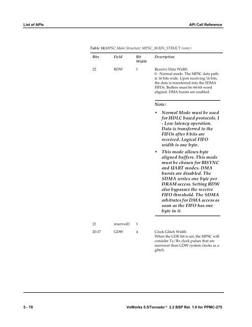
Table 14:MPSC Main Structure: MPSC_MAIN_STRUCT (cont.)<br />
Bits Field Bit<br />
Width<br />
22 RDW 1 Receive Data Width<br />
0 - Normal mode. The MPSC data path<br />
is 16 bits wide. Upon receiving 16 bits,<br />
the data is transferred into the SDMA<br />
FIFOs. Buffers must be 64-bit word<br />
aligned. DMA bursts are enabled.<br />
21 reserved1 1<br />
Description<br />
Note:<br />
• Normal Mode must be used<br />
<strong>for</strong> HDLC based protocols. 1<br />
- Low latency operation.<br />
Data is transferred to the<br />
FIFOs after 8 bits are<br />
received. Logical FIFO<br />
width is one byte.<br />
• This mode allows byte<br />
aligned buffers. This mode<br />
must be chosen <strong>for</strong> BISYNC<br />
and UART modes. DMA<br />
bursts are disabled. The<br />
SDMA writes one byte per<br />
DRAM access. Setting RDW<br />
also bypasses the receive<br />
FIFO threshold. The SDMA<br />
arbitrates <strong>for</strong> DMA access as<br />
soon as the FIFO has one<br />
byte in it.<br />
20:17 GDW 4 Clock Glitch Width<br />
When the GDE bit is set, the MPSC will<br />
consider Tx/Rx clock pulses that are<br />
narrower than GDW system clocks as a<br />
glitch.<br />
5 - 78 VxWorks 5.5/Tornado <strong>2.2</strong> <strong>BSP</strong> <strong>Rel</strong>. <strong>1.0</strong> <strong>for</strong> <strong>PPMC</strong>-<strong>275</strong>