2.2 BSP Rel. 1.0 for PPMC-275 Programmer's Guide
2.2 BSP Rel. 1.0 for PPMC-275 Programmer's Guide
2.2 BSP Rel. 1.0 for PPMC-275 Programmer's Guide
You also want an ePaper? Increase the reach of your titles
YUMPU automatically turns print PDFs into web optimized ePapers that Google loves.
List of APIs API Call Reference<br />
use the value of 0 by default <strong>for</strong> this parameter), Device number on<br />
the bus, Function number within the device (will be combined<br />
with the register offset) and Configuration register offset within<br />
the device/function being accessed. A subsequent read to the PCI<br />
Configuration Data register causes the GT to translate that Configuration<br />
Address value to the requested cycle on the PCI bus (in<br />
this case - read) or internal configuration space. This function<br />
reads from an agent’s configuration register at any of the eight<br />
possible function in its Configuration Space Header.<br />
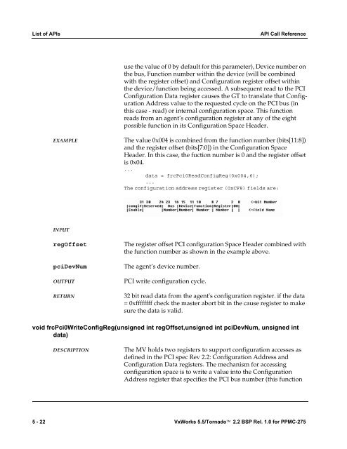
EXAMPLE The value 0x004 is combined from the function number (bits[11:8])<br />
and the register offset (bits[7:0]) in the Configuration Space<br />
Header. In this case, the fuction number is 0 and the register offset<br />
is 0x04.<br />
...<br />
data = frcPci0ReadConfigReg(0x004,6);<br />
...<br />
The configuration address register (0xCF8) fields are:<br />
INPUT<br />
regOffset The register offset PCI configuration Space Header combined with<br />
the function number as shown in the example above.<br />
pciDevNum The agent’s device number.<br />
OUTPUT PCI write configuration cycle.<br />
RETURN 32 bit read data from the agent's configuration register. if the data<br />
= 0xffffffff check the master abort bit in the cause register to make<br />
sure the data is valid.<br />
void frcPci0WriteConfigReg(unsigned int regOffset,unsigned int pciDevNum, unsigned int<br />
data)<br />
DESCRIPTION The MV holds two registers to support configuration accesses as<br />
defined in the PCI spec Rev <strong>2.2</strong>: Configuration Address and<br />
Configuration Data registers. The mechanism <strong>for</strong> accessing<br />
configuration space is to write a value into the Configuration<br />
Address register that specifies the PCI bus number (this function<br />
5 - 22 VxWorks 5.5/Tornado <strong>2.2</strong> <strong>BSP</strong> <strong>Rel</strong>. <strong>1.0</strong> <strong>for</strong> <strong>PPMC</strong>-<strong>275</strong>


