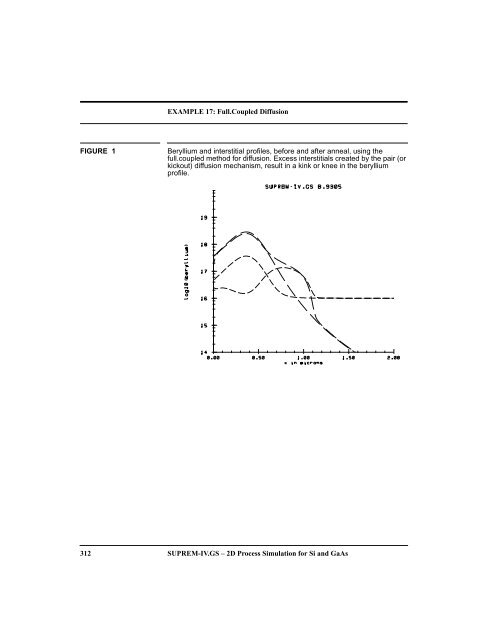
EXAMPLE 17: Full.Coupled Diffusion 312 SUPREM-IV.GS – 2D ...
EXAMPLE 17: Full.Coupled Diffusion 312 SUPREM-IV.GS – 2D ...
EXAMPLE 17: Full.Coupled Diffusion 312 SUPREM-IV.GS – 2D ...

Create successful ePaper yourself
Turn your PDF publications into a flip-book with our unique Google optimized e-Paper software.
<strong>EXAMPLE</strong> <strong>17</strong>: <strong>Full</strong>.<strong>Coupled</strong> <strong>Diffusion</strong><br />
FIGURE 1 Beryllium and interstitial profiles, before and after anneal, using the<br />
full.coupled method for diffusion. Excess interstitials created by the pair (or<br />
kickout) diffusion mechanism, result in a kink or knee in the beryllium<br />
profile.<br />
<strong>312</strong> <strong>SUPREM</strong>-<strong>IV</strong>.<strong>GS</strong> <strong>–</strong> <strong>2D</strong> Process Simulation for Si and GaAs
<strong>EXAMPLE</strong> <strong>17</strong>: <strong>Full</strong>.<strong>Coupled</strong> <strong>Diffusion</strong><br />
diffuse time=.00001 temp=800 argon<br />
In this first diffusion step, a short time anneal is done to establish the equi-<br />
librium defect concentrations in case you want to plot the initial values of<br />
these (since they are temperature dependent). In the second diffuse state-<br />
ment:<br />
diffuse time=15 temp=800 continue argon<br />
the continue parameter is used to maintain the initial defect values. There-<br />
fore, the initial diffuse uses the fermi method, and the defect levels are ini-<br />
tially set at their equilibrium values. (Since the interstitials are set at the +1<br />
charge state, the equilibrium interstitial concentration is fermi level depen-<br />
dent and therefore the initial interstitial profile follows the beryllium pro-<br />
file). The main diffusion step uses the full.cpl method. The dopant/defect<br />
pairing parameters are specified by the following statements.<br />
interstitial gaas beryllium neu.0=0 pos.0=0 neg.0=0<br />
dneg.0=0 dpos.0=0<br />
interstitial gaas beryllium tneg.0=0 tpos.0=0<br />
These are all normally set to 0 if one assumes that the pair concentration is<br />
much less than the defect concentration (non-equilibrium levels of defects<br />
will still occur, since the defect flux equation in the full-coupled mode still<br />
takes into account the extra defects produced by the diffusion process). In<br />
Figure 1, the as-implanted and diffused beryllium and interstitial profiles<br />
generated are shown. One can see that, compared to Example 13, a kink in<br />
the profile occurs due to this defect non-equilibrium effect. If one increas-<br />
es the interstitial diffusivity in the statement:<br />
interstitial gaas D.0=5e-14 D.E= 0.<br />
from 5 10 -14 to 1 10 -11 for example, the interstitials are able to diffuse<br />
back to their equilibrium levels everywhere, and normal “Example 13<br />
type” diffusion occurs.<br />
<strong>SUPREM</strong>-<strong>IV</strong>.<strong>GS</strong> <strong>–</strong> <strong>2D</strong> Process Simulation for Si and GaAs 311
<strong>EXAMPLE</strong> <strong>17</strong>: <strong>Full</strong>.<strong>Coupled</strong> <strong>Diffusion</strong><br />
vacancy dpos.0=0 dpos.E=0 neg.E=0 tpos.0=0 tneg.0=1<br />
vacancy gaas beryllium neu.0=0 pos.0=0 neg.0=0<br />
dneg.0=0 dpos.0=0<br />
vacancy gaas beryllium tneg.0=0 tpos.0=0<br />
method full.fac<br />
diffuse time=.00001 temp=800 argon<br />
select z=log10(beryllium)<br />
plot.1d x.min=0 x.ma=2 y.mi=14 y.max=20<br />
line.type=4<br />
select z=log10(inter)<br />
plot.1d x.min=0 x.ma=2 y.mi=14 y.max=20 cle=f<br />
axi=f line.type=2<br />
method full.cpl init=1e-5<br />
diffuse time=15 temp=800 continue argon<br />
select z=log10(beryllium)<br />
plot.1d x.min=0 x.ma=2 y.mi=14 y.max=20 cle=f<br />
axi=f line.type=4<br />
select z=log10(inter)<br />
plot.1d x.min=0 x.ma=2 y.mi=14 y.max=20 cle=f<br />
axi=f line.type=2<br />
quit<br />
Here Example 13 is repeated, but using the full.coupled diffusion method<br />
rather than the fermi method. In this method, non-equilibrium levels of in-<br />
terstitials or vacancies can be produced by the diffusion process itself,<br />
without adding non-equilibrium levels of defects at the beginning, as was<br />
done in Example 16. This is because in the diffusion process, the dopant<br />
diffuses as a dopant/defect pair, and defects are carried along with the<br />
dopant. This can result in local regions of non-equilibrium concentrations<br />
of defects and can in turn effect the dopant diffusion. (If one believes that<br />
the “kick-out” mechanism is occurring rather than the pair mechanism, the<br />
same effect occurs as the interstitial dopant kicks-out a matrix atom, creat-<br />
ing an interstitial.) The method statement is now:<br />
method full.cpl init=1e-5<br />
Note that there is an initial very short diffuse statement:<br />
310 <strong>SUPREM</strong>-<strong>IV</strong>.<strong>GS</strong> <strong>–</strong> <strong>2D</strong> Process Simulation for Si and GaAs
<strong>EXAMPLE</strong> <strong>17</strong>: <strong>Full</strong>.<strong>Coupled</strong> <strong>Diffusion</strong><br />
<strong>EXAMPLE</strong> <strong>17</strong> <strong>Full</strong>.<strong>Coupled</strong> <strong>Diffusion</strong><br />
The input file for the simulation is in the “examples/exam<strong>17</strong>” directory, in<br />
the file example<strong>17</strong>.in. In this example, the full.coupled method of diffu-<br />
sion is illustrated.<br />
option quiet<br />
set echo<br />
mode one.dim<br />
line x loc=0.0 spacing=0.01 tag=top<br />
line x loc=1.0 spacing=0.01<br />
line x loc=20 spacing=0.25 tag=bottom<br />
region gaas xlo=top xhi=bottom<br />
boundary exposed xlo=top xhi=top<br />
boundary backside xlo=bottom xhi=bottom<br />
init carbon conc=1e15<br />
implant beryllium dose=1e14 energy=100 pearson<br />
deposit nitride thick=.3<br />
interstitial gaas D.0=5e-14 D.E= 0.<br />
interstitial gaas Kr.0=1e-18 Kr.E= 0.<br />
interstitial gaas Cstar.0= 1.0e16 Cstar.E= 0.<br />
interstitial gaas /nitride Ksurf.0= 1e-3 Ksurf.E= 0.<br />
interstitial gaas neu.0=0 pos.0=1 neu.E=0 neg.0=0<br />
pos.E=0 dneg.0=0<br />
interstitial gaas dpos.0=0 dpos.E=0 neg.E=0 tpos.0=0<br />
tneg.0=0<br />
interstitial gaas beryllium neu.0=0 pos.0=0 neg.0=0<br />
dneg.0=0 dpos.0=0<br />
interstitial gaas beryllium tneg.0=0 tpos.0=0<br />
vacancy gaas D.0= 1e-15 D.E= 0.<br />
vacancy gaas Kr.0=1e-18 Kr.E= 0.<br />
vacancy gaas Cstar.0= 1e16 Cstar.E= 0.<br />
vacancy gaas /nitride Ksurf.0= 1e-3 Ksurf.E= 0.<br />
vacancy gaas neu.0=0 pos.0=0 neu.E=0 neg.0=0 pos.E=0<br />
dneg.0=0<br />
<strong>SUPREM</strong>-<strong>IV</strong>.<strong>GS</strong> <strong>–</strong> <strong>2D</strong> Process Simulation for Si and GaAs 309
<strong>EXAMPLE</strong> 16: Two.Dim <strong>Diffusion</strong> With File Input Interstitials<br />
308 <strong>SUPREM</strong>-<strong>IV</strong>.<strong>GS</strong> <strong>–</strong> <strong>2D</strong> Process Simulation for Si and GaAs
<strong>EXAMPLE</strong> 16: Two.Dim <strong>Diffusion</strong> With File Input Interstitials<br />
is used, rather than the fermi method statement. Parameters for various in-<br />
terstitial and vacancy properties are also included. For example, only +1<br />
charge state interstitials are used, according to the statements:<br />
interstitial gaas neu.0=0 pos.0=1 neu.E=0 neg.0=0<br />
pos.E=0 dneg.0=0<br />
interstitial gaas dpos.0=0 dpos.E=0 neg.E=0 tpos.0=0<br />
tneg.0=0<br />
The as-implanted and diffused profiles of beryllium and interstitials are<br />
shown in Figure 1. The diffused beryllium profile is much different than<br />
that in Example 13, where the fermi method was used (with no added in-<br />
terstitials). The simulation predicts the famous “uphill diffusion” of im-<br />
planted p-type dopants often observed.<br />
FIGURE 1 Beryllium and interstitial profiles, before and after anneal, using the two.dim<br />
method for diffusion. The excess interstitials (above I * ) produce “uphill<br />
diffusion” of Beryllium.<br />
<strong>SUPREM</strong>-<strong>IV</strong>.<strong>GS</strong> <strong>–</strong> <strong>2D</strong> Process Simulation for Si and GaAs 307
<strong>EXAMPLE</strong> 16: Two.Dim <strong>Diffusion</strong> With File Input Interstitials<br />
method full.fac<br />
select z=log10(beryllium)<br />
plot.1d x.min=0 x.ma=2 y.mi=14 y.max=20<br />
line.type=4<br />
select z=log10(inter)<br />
plot.1d x.min=0 x.ma=2 y.mi=14 y.max=20 cle=f<br />
axi=f line.type=2<br />
method two.dim init=1e-5<br />
diffuse time=15 temp=800 argon<br />
select z=log10(beryllium)<br />
plot.1d x.min=0 x.ma=2 y.mi=14 y.max=20 cle=f<br />
axi=f line.type=4<br />
select z=log10(inter)<br />
plot.1d x.min=0 x.ma=2 y.mi=14 y.max=20 cle=f<br />
axi=f line.type=2<br />
quit<br />
In Example 13, the Fermi method for diffusion was used, in which it is as-<br />
sumed that interstitial and vacancy concentrations are at their equilibrium<br />
values throughout the simulation. Therefore, the diffusivities are only de-<br />
pendent on temperature and the local doping concentrations (n or p). In<br />
Example 14, the two.dim method for diffusion is used, in which extrinsic<br />
interstitials or vacancies (i.e. added from some source, such as implant<br />
damage, or from oxidation in the case of silicon technology) are taken into<br />
account in the diffusion of dopants. In this case I/I* or V/V* may not equal<br />
one, and these terms are included in the diffusion equations. In this exam-<br />
ple, the interstitial profile is input by the statement:<br />
profile infile=file1 inter<br />
where file1 contains the x concentration values for the interstitials that<br />
might be caused by implantation damage. Now the statement:<br />
method two.dim init=1e-5<br />
306 <strong>SUPREM</strong>-<strong>IV</strong>.<strong>GS</strong> <strong>–</strong> <strong>2D</strong> Process Simulation for Si and GaAs
<strong>EXAMPLE</strong> 16: Two.Dim <strong>Diffusion</strong> With File Input Interstitials<br />
<strong>EXAMPLE</strong> 16 Two.Dim <strong>Diffusion</strong> With File Input Interstitials<br />
Here the two.dim method for diffusion is illustrated. The input file for the<br />
simulation is in the “examples/exam16” directory, in the file exam-<br />
ple16.in.<br />
option quiet<br />
set echo<br />
mode one.dim<br />
line x loc=0.0 spacing=0.01 tag=top<br />
line x loc=1.0 spacing=0.01<br />
line x loc=20 spacing=0.25 tag=bottom<br />
region gaas xlo=top xhi=bottom<br />
boundary exposed xlo=top xhi=top<br />
boundary backside xlo=bottom xhi=bottom<br />
init carbon conc=1e15<br />
implant beryllium dose=1e14 energy=100 pearson<br />
profile infile=file1 inter<br />
deposit nitride thick=.3<br />
interstitial gaas D.0=5e-14 D.E= 0.<br />
interstitial gaas Kr.0=1e-18 Kr.E= 0.<br />
interstitial gaas Cstar.0= 1.0e16 Cstar.E= 0.<br />
interstitial gaas /nitride Ksurf.0= 1e-3 Ksurf.E=<br />
0.<br />
interstitial gaas neu.0=0 pos.0=1 neu.E=0 neg.0=0<br />
pos.E=0 dneg.0=0<br />
interstitial gaas dpos.0=0 dpos.E=0 neg.E=0 tpos.0=0<br />
tneg.0=0<br />
vacancy gaas D.0= 1e-15 D.E= 0.<br />
vacancy gaas Kr.0=1e-18 Kr.E= 0.<br />
vacancy gaas Cstar.0= 1e16 Cstar.E= 0.<br />
vacancy gaas /nitride Ksurf.0= 1e-3 Ksurf.E= 0.<br />
vacancy gaas neu.0=0 pos.0=0 neu.E=0 neg.0=0 pos.E=0<br />
dneg.0=0<br />
vacancy dpos.0=0 dpos.E=0 neg.E=0 tpos.0=0 tneg.0=1<br />
<strong>SUPREM</strong>-<strong>IV</strong>.<strong>GS</strong> <strong>–</strong> <strong>2D</strong> Process Simulation for Si and GaAs 305
<strong>EXAMPLE</strong> 15: Annealing An Implant From Measured (SIMS) Data<br />
profile infile=be1 beryllium<br />
File be1 contains the x concentration values for the as-implanted berylli-<br />
um profile. In order to use the “implanted” diffusivities even though there<br />
is no implant statement a “dummy” implant is done,<br />
implant beryllium dose=1e1 energy=100 pearson<br />
in which a very low dose beryllium implant is used. As shown in Figure 1,<br />
the extent of diffusion is comparable to that of Example 13, and much<br />
more than in Example 14, indicating the higher “implanted” diffusivity is<br />
used.<br />
FIGURE 1 Implanted beryllium from SIMS data and <strong>SUPREM</strong>-<strong>IV</strong>.<strong>GS</strong> annealed profile.<br />
304 <strong>SUPREM</strong>-<strong>IV</strong>.<strong>GS</strong> <strong>–</strong> <strong>2D</strong> Process Simulation for Si and GaAs
<strong>EXAMPLE</strong> 15: Annealing An Implant From Measured (SIMS) Data<br />
<strong>EXAMPLE</strong> 15 Annealing An Implant From Measured (SIMS)<br />
Data<br />
In this example, the “implanted” diffusivities are used, even though there<br />
is no implant statement. The input file for the simulation is in the “exam-<br />
ples/exam15” directory, in the file example15.in.<br />
option quiet<br />
set echo<br />
mode one.dim<br />
line x loc=0.0 spacing=0.01 tag=top<br />
line x loc=1.0 spacing=0.01<br />
line x loc=20 spacing=0.25 tag=bottom<br />
region gaas xlo=top xhi=bottom<br />
boundary exposed xlo=top xhi=top<br />
boundary backside xlo=bottom xhi=bottom<br />
init carbon conc=1e15<br />
profile infile=be1 beryllium<br />
implant beryllium dose=1e1 energy=100 pearson<br />
deposit nitride thick=.3<br />
select z=log10(beryllium)<br />
plot.1d x.min=0 x.ma=2 y.mi=14 y.max=20<br />
line.type=4<br />
method fermi init=1e-5<br />
method full.fac<br />
diffuse time=15 temp=800 argon<br />
select z=log10(beryllium)<br />
plot.1d x.min=0 x.ma=2 y.mi=14 y.max=20 cle=f<br />
axi=f line.type=2<br />
quit<br />
The as-implanted profile obtained from SIMS measurements is input from<br />
a file (“be1”) by using the profile statement:<br />
<strong>SUPREM</strong>-<strong>IV</strong>.<strong>GS</strong> <strong>–</strong> <strong>2D</strong> Process Simulation for Si and GaAs 303
<strong>EXAMPLE</strong> 14: Grown-in and Annealed Beryllium<br />
deposit gaas thick=.5 divisions=100 beryllium<br />
conc=1e15<br />
instead of an implant statement. In this case, <strong>SUPREM</strong>-<strong>IV</strong>.<strong>GS</strong> uses the<br />
lower “as-grown” diffusivities for beryllium since no implanted beryllium<br />
is present. The as-grown and diffused profiles are shown in Figure 5. The<br />
extent of beryllium diffusion is seen to be much less in this case compared<br />
to the implanted case (Example 13), even though the same anneal condi-<br />
tions are used and the beryllium peak concentrations are comparable (the<br />
diffusion is hole, or concentration, dependent).<br />
FIGURE 1 Grown-in and annealed beryllium in GaAs using the grown-in diffusion<br />
coefficients.<br />
302 <strong>SUPREM</strong>-<strong>IV</strong>.<strong>GS</strong> <strong>–</strong> <strong>2D</strong> Process Simulation for Si and GaAs
<strong>EXAMPLE</strong> 14: Grown-in and Annealed Beryllium<br />
<strong>EXAMPLE</strong> 14 Grown-in and Annealed Beryllium<br />
The input file for this simulation is in the “examples/exam14” directory, in<br />
the file example14.in.<br />
option quiet<br />
set echo<br />
mode one.dim<br />
line x loc=0.0 spacing=0.01 tag=top<br />
line x loc=1.0 spacing=0.01<br />
line x loc=20 spacing=0.25 tag=bottom<br />
region gaas xlo=top xhi=bottom<br />
boundary exposed xlo=top xhi=top<br />
boundary backside xlo=bottom xhi=bottom<br />
init beryllium conc=1e15<br />
deposit gaas thick=.5 divisions=100 beryllium<br />
conc=5e18<br />
deposit gaas thick=.5 divisions=100 beryllium<br />
conc=1e15<br />
deposit nitride thick=.3<br />
select z=log10(beryllium)<br />
plot.1d x.min=-1 x.ma=1 y.mi=14 y.max=20<br />
line.type=4<br />
method fermi init=1e-5<br />
method full.fac<br />
diffuse time=15 temp=800 argon<br />
select z=log10(beryllium)<br />
plot.1d x.min=-1 x.ma=1 y.mi=14 y.max=20 cle=f<br />
axi=f line.type=2<br />
quit<br />
Here, Be is grown into the GaAs by using the deposit statements<br />
deposit gaas thick=.5 divisions=100 beryllium<br />
conc=5e18<br />
<strong>SUPREM</strong>-<strong>IV</strong>.<strong>GS</strong> <strong>–</strong> <strong>2D</strong> Process Simulation for Si and GaAs 301
<strong>EXAMPLE</strong> 13: Implanted and Annealed Beryllium<br />
FIGURE 1 Implanted and annealed beryllium using the implanted diffusion<br />
coefficients.<br />
300 <strong>SUPREM</strong>-<strong>IV</strong>.<strong>GS</strong> <strong>–</strong> <strong>2D</strong> Process Simulation for Si and GaAs
<strong>EXAMPLE</strong> 13: Implanted and Annealed Beryllium<br />
<strong>EXAMPLE</strong> 13 Implanted and Annealed Beryllium<br />
Examples 13, 14, and 15 illustrate the differences in using implanted vs.<br />
grown-in dopants, and how it effects the diffusivity values used. In<br />
Example 13, beryllium is implanted in GaAs, and the structure is an-<br />
nealed. The input file for the simulation is in the “examples/exam13” di-<br />
rectory, in the file example13.in. The as-implanted and diffused beryllium<br />
profiles are shown in Figure 1. The implanted diffusion coefficients are<br />
used since there is an “implant beryllium ...” statement.<br />
option quiet<br />
set echo<br />
mode one.dim<br />
line x loc=0.0 spacing=0.01 tag=top<br />
line x loc=1.0 spacing=0.01<br />
line x loc=20 spacing=0.25 tag=bottom<br />
region gaas xlo=top xhi=bottom<br />
boundary exposed xlo=top xhi=top<br />
boundary backside xlo=bottom xhi=bottom<br />
init carbon conc=1e15<br />
implant beryllium dose=1e14 energy=100 pearson<br />
deposit nitride thick=.3<br />
select z=log10(beryllium)<br />
plot.1d x.min=0 x.ma=2 y.mi=14 y.max=20<br />
line.type=4<br />
method fermi init=1e-5<br />
method full.fac<br />
diffuse time=15 temp=800 argon<br />
select z=log10(beryllium)<br />
plot.1d x.mi=0 x.ma=2 y.mi=14 y.ma=20 cle=f axi=f<br />
line.typ=2<br />
quit<br />
<strong>SUPREM</strong>-<strong>IV</strong>.<strong>GS</strong> <strong>–</strong> <strong>2D</strong> Process Simulation for Si and GaAs 299
<strong>EXAMPLE</strong> 12: Dopant Activation Model Example<br />
FIGURE 2 Same as Figure 1 except that modified silicon activation numbers are used,<br />
resulting in a higher silicon activation.<br />
298 <strong>SUPREM</strong>-<strong>IV</strong>.<strong>GS</strong> <strong>–</strong> <strong>2D</strong> Process Simulation for Si and GaAs
<strong>EXAMPLE</strong> 12: Dopant Activation Model Example<br />
FIGURE 1 Silicon, electrons, and net doping profiles for a silicon/beryllium MESFET<br />
structure. The default activation models are used for silicon.<br />
<strong>SUPREM</strong>-<strong>IV</strong>.<strong>GS</strong> <strong>–</strong> <strong>2D</strong> Process Simulation for Si and GaAs 297
<strong>EXAMPLE</strong> 12: Dopant Activation Model Example<br />
Silicon is implanted into GaAs with a beryllium doped background.<br />
Figure 1 shows the 1D plot of this. The default n and p-type activation<br />
models are used, commented out in the lines:<br />
#material gaas p.type act.a="(2.2 - 0.001<strong>17</strong> * T)"<br />
act.b="1.00e21"<br />
#material gaas n.type act.a="(2.2 - 0.001<strong>17</strong> * T)"<br />
act.b="4.25e18"<br />
Plotted in Figure 1 are the silicon profile, the electron profile, and the net<br />
doping profile. The electron profile takes into account the less than 100<br />
percent net n-type dopant activation under the silicon peak, as well as the<br />
reduced electron concentration in the bulk due to the beryllium back-<br />
ground doping. The abs(doping) profile clearly shows the silicon/berylli-<br />
um n/p junction.<br />
Figure 2 shows the results when the n-type activation model parameters<br />
are changed. In this case, the following line is included:<br />
material gaas n.type act.a="(2.2 - 0.001<strong>17</strong> * T)"<br />
act.b="4.25e18"<br />
Note that the act.b parameter has been changed. This increases the net ac-<br />
tive n-type dopant concentration under the peak of the silicon implant pro-<br />
file.<br />
296 <strong>SUPREM</strong>-<strong>IV</strong>.<strong>GS</strong> <strong>–</strong> <strong>2D</strong> Process Simulation for Si and GaAs
<strong>EXAMPLE</strong> 12: Dopant Activation Model Example<br />
<strong>EXAMPLE</strong> 12 Dopant Activation Model Example<br />
Here the <strong>SUPREM</strong>-<strong>IV</strong>.<strong>GS</strong> dopant activation model is illustrated. The input<br />
file for the simulation is in the “examples/exam12” directory, in the file ex-<br />
ample12.in.<br />
option quiet<br />
set echo<br />
mode one.dim<br />
line x loc=0.0 spacing=0.02 tag=top<br />
line x loc=0.5 spacing=0.02<br />
line x loc=20 spacing=0.25 tag=bottom<br />
region gaasxlo=top xhi=bottom<br />
boundary exposed xlo=top xhi=top<br />
boundary backside xlo=bottom xhi=bottom<br />
init beryllium conc=3e<strong>17</strong><br />
implant isilicon dose=5e13 energy=100 pearson<br />
#material gaas p.type act.a="(2.2 - 0.001<strong>17</strong> * T)"<br />
act.b="1.00e21"<br />
#material gaas n.type act.a="(2.2 - 0.001<strong>17</strong> * T)"<br />
act.b="4.25e18"<br />
deposit nitride thick=.3<br />
method fermi init=1e-5<br />
diffuse time=.001 temp=750 argon<br />
select z=log10(isilicon)<br />
plot.1d x.mi=0 x.ma=2 y.mi=14 y.ma=20 line.type=1<br />
select z=log10(electrons)<br />
plot.1d x.mi=0 x.ma=2 y.mi=14 y.ma=20 cle=f axi=f<br />
line.type=2<br />
select z=log10(abs(doping))<br />
plot.1d x.mi=0 x.ma=2 y.mi=14 y.ma=20 cle=f axi=f<br />
line.type=3<br />
quit<br />
<strong>SUPREM</strong>-<strong>IV</strong>.<strong>GS</strong> <strong>–</strong> <strong>2D</strong> Process Simulation for Si and GaAs 295
<strong>EXAMPLE</strong> 11: GaAs Simulation <strong>–</strong> <strong>2D</strong><br />
294 <strong>SUPREM</strong>-<strong>IV</strong>.<strong>GS</strong> <strong>–</strong> <strong>2D</strong> Process Simulation for Si and GaAs
<strong>EXAMPLE</strong> 11: GaAs Simulation <strong>–</strong> <strong>2D</strong><br />
FIGURE 1 Beryllium and Silicon contours in the MESFET source, drain, and channel<br />
regions.<br />
<strong>SUPREM</strong>-<strong>IV</strong>.<strong>GS</strong> <strong>–</strong> <strong>2D</strong> Process Simulation for Si and GaAs 293
<strong>EXAMPLE</strong> 11: GaAs Simulation <strong>–</strong> <strong>2D</strong><br />
implant beryllium dose=1e13 energy=100 pearson<br />
etch nitride start x=4.5 y=0.0<br />
etch continue x=4.5 y=-1.10<br />
etch continue x=0 y=-1.10<br />
etch done x=0 y=0.0<br />
deposit nitride thick=1.0<br />
etch nitride start x=4.5 y=0.0<br />
etch continue x=4.5 y=-1.10<br />
etch continue x=0.0 y=-1.10<br />
etch done x=0.0 y=0.0<br />
implant isilicon dose=1e13 energy=100.0 pearson<br />
etch nitride start x=4.5 y=0.0<br />
etch continue x=4.5 y=-1.10<br />
etch continue x=5.0 y=-1.10<br />
etch done x=5.0 y=0.0<br />
deposit nitride thick=.05<br />
structure mirror right<br />
plot.2d bound fill x.min=4.0 x.max=6 y.max=1.6<br />
select z=log10(isilicon)<br />
foreach v (15. to 18.5 step 0.5)<br />
contour val=v line.type=2<br />
end<br />
plot.2d bound fill x.min=4 x.max=6 y.max=1.6 cle=f<br />
axi=f<br />
select z=log10(beryllium)<br />
foreach v (16.5 to <strong>17</strong>.0 step .5)<br />
contour val=v line.type=4<br />
end<br />
quit<br />
292 <strong>SUPREM</strong>-<strong>IV</strong>.<strong>GS</strong> <strong>–</strong> <strong>2D</strong> Process Simulation for Si and GaAs
<strong>EXAMPLE</strong> 11: GaAs Simulation <strong>–</strong> <strong>2D</strong><br />
<strong>EXAMPLE</strong> 11 GaAs Simulation <strong>–</strong> <strong>2D</strong><br />
This shows how one would do a <strong>2D</strong> GaAs simulation. A <strong>2D</strong> grid is set up,<br />
and silicon and beryllium are implanted in the source, drain and channel<br />
regions. Then the doping contours are plotted for the designated concen-<br />
tration levels in Figure 2. In this example, only one half of the structure is<br />
simulated, then mirrored before the result is plotted, in order to speed up<br />
simulation time. The input file for the simulation is in the “examples/<br />
exam11” directory, in the file example11.in.<br />
option quiet<br />
set echo<br />
line x loc = 0.0 tag=left spacing = 0.5<br />
line x loc = 0.50 spacing = 0.5<br />
line x loc = 4.00 spacing = 0.5<br />
line x loc = 4.10 spacing = 0.1<br />
line x loc = 4.20 spacing = 0.05<br />
line x loc = 4.50 spacing = 0.05<br />
line x loc = 5.00 tag=right spacing = 0.05<br />
line y loc=0.0 tag=top spacing=0.03<br />
line y loc=0.3 spacing=0.03<br />
line y loc=1.0 spacing=0.1<br />
line y loc=3.0 tag=bottom spacing=0.3<br />
region gaas xlo=left xhi=right ylo=top yhi=bottom<br />
boundary exposed xlo=left xhi=right ylo=top yhi=top<br />
boundary backside xlo=left xhi=right ylo=bottom yhi=bottom<br />
init isilicon conc=3e15<br />
deposit nitride thick=1.0<br />
etch nitride start x=5 y=0.0<br />
etch continue x=5 y=-1.10<br />
etch continue x=4.5 y=-1.10<br />
etch done x=4.5 y=0.0<br />
implant isilicon dose=1.75e12 energy=75 pearson<br />
<strong>SUPREM</strong>-<strong>IV</strong>.<strong>GS</strong> <strong>–</strong> <strong>2D</strong> Process Simulation for Si and GaAs 291
<strong>EXAMPLE</strong> 10: GaAs MESFET Gate Simulation <strong>–</strong> 1D<br />
290 <strong>SUPREM</strong>-<strong>IV</strong>.<strong>GS</strong> <strong>–</strong> <strong>2D</strong> Process Simulation for Si and GaAs
<strong>EXAMPLE</strong> 10: GaAs MESFET Gate Simulation <strong>–</strong> 1D<br />
FIGURE 1 Beryllium, Silicon, and Carbon profiles under the MESFET gate.<br />
<strong>SUPREM</strong>-<strong>IV</strong>.<strong>GS</strong> <strong>–</strong> <strong>2D</strong> Process Simulation for Si and GaAs 289
<strong>EXAMPLE</strong> 10: GaAs MESFET Gate Simulation <strong>–</strong> 1D<br />
select z=log10(beryllium)<br />
plot.1d x.min=0 x.ma=2 y.mi=14 y.max=20<br />
line.type=2<br />
select z=log10(isilicon)<br />
plot.1d x.min=0 x.ma=2 y.mi=14 y.max=20 cle=f<br />
axi=f line.type=3<br />
select z=log10(carbon)<br />
plot.1d x.min=0 x.ma=2 y.mi=14 y.max=20 cle=f<br />
axi=f line.type=4<br />
method fermi init=1e-5<br />
method full.fac<br />
diffuse time=15 temp=800 argon<br />
select z=log10(beryllium)<br />
plot.1d x.min=0 x.ma=2 y.mi=14 y.max=20 cle=f<br />
axi=f line.type=5<br />
quit<br />
If you wish to change the beryllium diffusivity parameters, you would un-<br />
comment the line:<br />
#beryllium gaas Dip.0=2.1e-8 Dip.E=1.74<br />
and put in your own values.<br />
288 <strong>SUPREM</strong>-<strong>IV</strong>.<strong>GS</strong> <strong>–</strong> <strong>2D</strong> Process Simulation for Si and GaAs
<strong>EXAMPLE</strong> 10: GaAs MESFET Gate Simulation <strong>–</strong> 1D<br />
<strong>EXAMPLE</strong> 10 GaAs MESFET Gate Simulation <strong>–</strong> 1D<br />
DESCRIPTION<br />
This example simulates a simple 1D GaAs MESFET structure underneath<br />
the gate. This utilizes <strong>SUPREM</strong>-<strong>IV</strong>.<strong>GS</strong>'s new true 1D mode. First, the 1D<br />
grid is set up and initialized with carbon as a background dopant. Berylli-<br />
um and silicon are implanted into GaAs. Note that silicon as an impurity is<br />
designated as “isilicon”. The as-implanted dopant concentration-depth<br />
profiles are plotted in 1D in Figure 1. Next an anneal step is done, using<br />
the Fermi method, and the diffused beryllium profile is then plotted in the<br />
same figure. The hump in the beryllium profile at the beryllium/silicon<br />
junction is due to the electric field effect on diffusion. Since the beryllium<br />
was implanted, the implanted diffusivity numbers (as opposed to the<br />
grown-in numbers) are used. The input file for the simulation is in the<br />
“examples/exam10” directory, in the file example10.in.<br />
option quiet<br />
set echo<br />
mode one.dim<br />
line x loc=0.0 spacing=0.01 tag=top<br />
line x loc=1.0 spacing=0.01<br />
line x loc=20 spacing=0.25 tag=bottom<br />
region gaas xlo=top xhi=bottom<br />
boundary exposed xlo=top xhi=top<br />
boundary backside xlo=bottom xhi=bottom<br />
init carbon conc=1e15<br />
implant beryllium dose=2e13 energy=100 pearson<br />
implant isilicon dose=5e13 energy=50 pearson<br />
#beryllium gaas Dip.0=2.1e-8 Dip.E=1.74<br />
beryllium gaas /nitride Seg.0=.5 Seg.E=0<br />
deposit nitride thick=.3<br />
<strong>SUPREM</strong>-<strong>IV</strong>.<strong>GS</strong> <strong>–</strong> <strong>2D</strong> Process Simulation for Si and GaAs 287
<strong>EXAMPLE</strong> 9: Stress Dependent Oxidation<br />
FIGURE 2 Comparison of LOCOS Shapes with 500<br />
References<br />
1. 1. N. Guillemot, G. Pananakakis and P. Chenevier, IEEE Transactions<br />
on Electron Devices, ED-34, (1987).<br />
2. 2. D.-B. Kao, J. P. McVittie, W. D. Nix and K. C. Saraswat, “Two-Dimensional<br />
Silicon Oxidation Experiments and Theory,” IEDM Tech.<br />
Digest, 1985,<br />
286 <strong>SUPREM</strong>-<strong>IV</strong>.<strong>GS</strong> <strong>–</strong> <strong>2D</strong> Process Simulation for Si and GaAs
<strong>EXAMPLE</strong> 9: Stress Dependent Oxidation<br />
FIGURE 1 Comparison of LOCOS Shapes with 500<br />
<strong>SUPREM</strong>-<strong>IV</strong>.<strong>GS</strong> <strong>–</strong> <strong>2D</strong> Process Simulation for Si and GaAs 285
<strong>EXAMPLE</strong> 9: Stress Dependent Oxidation<br />
The third Newton step (#4) reduces the error by a large factor, so on the<br />
subsequent step not only is the length increased back to 1 but the same Ja-<br />
cobian is recycled, indicated by the asterisk. The recycled Jacobian proves<br />
not to be effective, since the error only goes from 1.6e-5 to 1.4e-5. One<br />
more Jacobian is factored, and causes an update of 0.0004636, less than<br />
the accuracy criterion. The first nonlinear problem has been solved.<br />
The stress-dependent reaction rate is then turned on (continuation to 0.5).<br />
In this case, the Newton process fails. Successively smaller steps along the<br />
Newton direction are taken, but at each attempted new position the error is<br />
larger than the current location. The smallest step tried is 0.031; the next<br />
would be 0.031/4 which is less than 1% of the Newton update and the sit-<br />
uation is considered hopeless. The program then backs off by trying an in-<br />
termediate lambda of 0.375. This corresponds to a stress dependence<br />
which is only half as strong as the desired dependence. After 15 Newton<br />
steps, this weaker problem is solved. The solution is then used as an initial<br />
guess for the problem first tried, that with the full stress dependence<br />
(lambda = 0.5). The improved initial guess leads to a successful solution<br />
of the problem after 3 Newton steps. Finally, the stress-dependent diffu-<br />
sivity is turned on (lambda =1). Since the activation volume for diffusivity<br />
was left at 0, nothing of interest happens and the problem is solved after<br />
one loop. The total number of Newton loops is therefore about 24, com-<br />
pared to 1 for a linear problem. Thus the nonlinear problem is about 24<br />
times as expensive to solve as a linear problem.<br />
The different oxide shapes are shown in Figures 1 and 2. The thicker ni-<br />
tride clearly has the effect of reducing the bird's beak.<br />
284 <strong>SUPREM</strong>-<strong>IV</strong>.<strong>GS</strong> <strong>–</strong> <strong>2D</strong> Process Simulation for Si and GaAs
<strong>EXAMPLE</strong> 9: Stress Dependent Oxidation<br />
Newton loop 2 cut 1 upd 0.1005 orhs 0.02204<br />
rhs 0.02313<br />
&...<br />
Newton loop28 cut 0.5 upd 0.00263 orhs 0.0005139<br />
rhs 0.0002645<br />
Newton loop30 cut 1 upd 0.0009523 orhs 0.0002647<br />
rhs 1e-38<br />
Continuation step #0 to lambda = 0.5 step 0.125<br />
Newton loop 0 cut 1 upd 0.01423 orhs 0.01075<br />
rhs 0.008121<br />
Newton loop 2 cut 1 upd 0.002104 orhs 0.008299<br />
rhs 0.003507<br />
Newton loop 4 cut 1 upd 0.002404 orhs 0.003543<br />
rhs 0.007114<br />
Newton loop 4 cut 0.25 upd 0.002404 orhs 0.003543<br />
rhs 0.002892<br />
Newton loop 6 cut 0.25 upd 0.0007027 orhs 0.002888<br />
rhs 1e-38<br />
Continuation step #0 to lambda = 1 step 0.5<br />
Newton loop 0 cut 1 upd 0.0005<strong>17</strong>8 orhs 0.002156<br />
rhs 1e-38<br />
The nonlinear solver works by proceeding first from the linear solution.<br />
The linear solution takes exactly two Newton steps. The first has a large<br />
update step 0.9914, which reduces the error from 3.811 to 3.5e-15. The<br />
second Newton step 1.3e-12 then of course is trivial since the solution has<br />
been reached. The Newton loop counter is incremented by two whenever a<br />
new Jacobian is factorized, and by one when only the error is recalculated.<br />
The stress-dependent viscosity is turned on (continuation step 0 to lambda<br />
= 0.25). The first step is moderately large 0.008394 and causes the error to<br />
increase 0.00022 to 0.0003045. A quarter-step (cut 0.25) in that direction<br />
is tried, which is found to decrease the error from 0.00022 to 0.0001. This<br />
new position is accepted as worthwhile, and a second Newton step is taken<br />
from there. It is found to decrease the error from 0.0059 to 0.00012. Since<br />
this is successful, the cutback factor is increased back to 0.5.<br />
<strong>SUPREM</strong>-<strong>IV</strong>.<strong>GS</strong> <strong>–</strong> <strong>2D</strong> Process Simulation for Si and GaAs 283
<strong>EXAMPLE</strong> 9: Stress Dependent Oxidation<br />
meth viscous oxide.rel=1e-2<br />
The viscous model is chosen, because only this model takes stress effects<br />
into account. (Only the viscous model calculates stress accurately enough<br />
to feed back into the coefficients). The relative error criterion is chosen as<br />
1% in the velocities. The default of 10 -6 is rather tight and requires more<br />
CPU time.<br />
The diffuse statement is as usual.<br />
This input file was executed twice, once with 0.05 m of nitride and once<br />
with 0.15 m of nitride. The output contains the usual features, along with<br />
many lines as follows:<br />
Newton loop 0 cut 1 upd 0.9914 orhs 3.811<br />
rhs 3.534e-15<br />
Newton loop 1* cut 1 upd 1.322e-12 orhs 3.534e-15<br />
rhs 1e-38<br />
Continuation step #0 to lambda = 0.25 step 0.25<br />
Newton loop 0 cut 1 upd 0.008394 orhs 0.0002229<br />
rhs 0.0003045<br />
Newton loop 0 cut 0.25 upd 0.008394 orhs 0.0002229<br />
rhs 0.000135<br />
Newton loop 2 cut 0.25 upd 0.005944 orhs 0.0001278<br />
rhs 6.63e-05<br />
Newton loop 4 cut 0.5 upd 0.004301 orhs 6.479e-05<br />
rhs 1.638e-05<br />
Newton loop 5* cut 1 upd 0.002137 orhs 1.638e-05<br />
rhs 1.43e-05<br />
Newton loop 7 cut 1 upd 0.000463 orhs 1.625e-05<br />
rhs 1e-38<br />
Continuation step #0 to lambda = 0.5 step 0.25<br />
Newton loop 0 cut 1 upd 0.1527 orhs 0.0359<br />
rhs 0.04011<br />
...<br />
Newton loop 4 cut 0.031 upd 2.062 orhs 0.01961<br />
rhs 0.0199<br />
Continued too far, backing off.<br />
Continuation step #-1 to lambda = 0.375 step 0.125<br />
Newton loop 0 cut 1 upd 0.06759 orhs 0.02686<br />
rhs 0.02223<br />
282 <strong>SUPREM</strong>-<strong>IV</strong>.<strong>GS</strong> <strong>–</strong> <strong>2D</strong> Process Simulation for Si and GaAs
<strong>EXAMPLE</strong> 9: Stress Dependent Oxidation<br />
<strong>EXAMPLE</strong> 9 Stress Dependent Oxidation<br />
DESCRIPTION<br />
This example shows the use of the stress-dependent oxidation model. Ex-<br />
perimental LOCOS profiles are generally of two distinct types [1]. When<br />
the nitride mask is more than two to three times thicker than the pad oxide,<br />
the oxide/silicon interface and the oxide gas surface is kinked. For thinner<br />
nitride masks, the shape can be approximately be described by an error-<br />
function. The kinks were not observed in the first generation of oxidation<br />
simulators, because they result from stress effects on the growth coeffi-<br />
cients. Early oxidation programs did not take stress into account and found<br />
essentially identical oxide shapes irrespective of nitride thickness. This ex-<br />
ample shows how the stress-dependent model in <strong>SUPREM</strong>-<strong>IV</strong>.<strong>GS</strong> can pre-<br />
dict such second-order effects. The example is given in the file “sdep.s4”<br />
in the “examples/exam9” directory.<br />
The grid structure and nitride/oxide sandwich is very similar to the fully-<br />
recessed oxide example. The substrate grid is as sparse as possible (two<br />
lines). The lateral grid is a little coarse to compensate for the increased<br />
computation time used in the nonlinear model.<br />
The new statements are as follows:<br />
oxide stress.dep=t<br />
The nonlinear stress-dependent model is turned on. The default is to turn it<br />
off since it is much more expensive to run than the linear model.<br />
The activation volume for plastic flow Vc, for the stress-dependent reac-<br />
tion rate Vr, and for the diffusivity Vd, are taken from the defaults in the<br />
model file. The values used were derived by fitting Kao’s cylinder oxida-<br />
tion data [2].<br />
<strong>SUPREM</strong>-<strong>IV</strong>.<strong>GS</strong> <strong>–</strong> <strong>2D</strong> Process Simulation for Si and GaAs 281
<strong>EXAMPLE</strong> 8: Shear Stress<br />
FIGURE 1 Critical Shear Stress Contours.<br />
The largest lobe corresponds to the 10 m stripe. The result for the 5 m<br />
stripe lies so closely on top that it cannot be distinguished. Thus either can<br />
be a reasonable approximation for infinitely separated stripes. The 4 m<br />
and 2.5 m lobes are somewhat smaller. This shows that the shear stress<br />
fields from neighboring stripes tend to cancel each other in their overlap<br />
areas, reducing the influence of the nitride film somewhat.<br />
References<br />
1. E. A. Irene, J. Electronic Mat., 5(3), p. 287, (1976).<br />
2. S. M. Hu, “Film-edge-induced Stress in Silicon Substrates,” Appl.<br />
Phys. Lett, 32(1), p. 5, 1978<br />
280 <strong>SUPREM</strong>-<strong>IV</strong>.<strong>GS</strong> <strong>–</strong> <strong>2D</strong> Process Simulation for Si and GaAs
<strong>EXAMPLE</strong> 8: Shear Stress<br />
This calculates the stress distribution arising from the nitride initial stress.<br />
Stress arising from thermal expansion mismatch would be included by<br />
specifying a different temp2. Be warned that large thermal steps often<br />
bring into play many more complicated phenomena than the simple ther-<br />
mal expansion mismatch analyzed in <strong>SUPREM</strong>-<strong>IV</strong>.<strong>GS</strong>. For instance<br />
breakdown of film adhesion or structural change may occur, but are not<br />
taken into account in the program.<br />
The principal slip system in silicon is in the direction on 111<br />
planes. This corresponds to the xy shear force in the plane of the simula-<br />
tion. The value 3 10 7 is considered by Hu[2] to be the critical shear stress<br />
for slip in silicon. Dislocations found in regions where the shear stress is<br />
larger than that value will move under the stress field of the nitride film.<br />
Therefore when analyzing stress in the substrate, a principal concern is the<br />
extent of the xy equal to 3 10 7 contour.<br />
plot.2 bound x.mi=-2 x.ma=2 y.ma=4 cl=f<br />
select z=Sxy<br />
contour val=-3e7<br />
The contours of xy equal to 3 10 7 in the silicon are shown in Figure 1.<br />
The contour is a double lobe because the shear stress is related to the polar<br />
components of stress through xy = ( rr - ) sin 2 + r cos 2 rr<br />
sin 2 The function sin 2 is at a maximum around 45˚ from the vertical,<br />
and is zero at = 90˚. Both rr and cos 2 change sign moving from left to<br />
right, so that the sign of xy is the same throughout. This means that a dis-<br />
location which is being driven under the mask by the stress field will con-<br />
tinue to move in that direction after passing the mask edge. However as it<br />
passes through the center, the decrease in shear stress may leave it strand-<br />
ed under the mask edge. The figure shows that the area of influence of the<br />
nitride film is many times greater than its thickness, about 2 m horizon-<br />
tally, and 1.5 m vertically.<br />
<strong>SUPREM</strong>-<strong>IV</strong>.<strong>GS</strong> <strong>–</strong> <strong>2D</strong> Process Simulation for Si and GaAs 279
<strong>EXAMPLE</strong> 8: Shear Stress<br />
line y loc=2 spac=0.3<br />
line y loc=5 tag=b<br />
region silicon xlo=l xhi=r ylo=si yhi=b<br />
bound expos xlo=l xhi=r ylo=si yhi=si<br />
initial ori=111<br />
Quite a large piece of substrate is analyzed, starting with a space 10 m by<br />
5 m. The foreach loop chooses four different widths to examine the ef-<br />
fect of different stripe separations. The structure being simulated has re-<br />
flecting boundary conditions (no perpendicular displacement) on the left<br />
and right sides. Those boundary conditions correspond to a single instance<br />
of a repeating pattern of nitride stripes. When the stripes are widely sepa-<br />
rated, there is little interference between the stress field of one stripe and<br />
the next, and the results are found to be independent of the stripe separa-<br />
tion. At smaller separations, the patterns begin to overlap. This example<br />
will show the stress pattern for widely separated stripes and the modifica-<br />
tions that occur as the stripes are brought closer together.<br />
The backside of the wafer also has a reflecting boundary condition. Al-<br />
though that approximation is not quite physical, the nitride film primarily<br />
exerts a horizontal force on the substrate, the assumption does not serious-<br />
ly affect the result. This can be verified by using different backside thick-<br />
nesses; 2 m or 100 m gives identical results. The exposed surface is the<br />
only surface with free displacements. The spacing around the film edge is<br />
0.1 m. This could be reduced for more accuracy, at the cost of more cpu<br />
time.<br />
deposit nitride thick=0.02 div=2<br />
etch nitride left p1.x = 0<br />
The nitride is deposited directly on silicon and patterned.<br />
material intrin.sig = 1.4e10 nitride<br />
The initial nitride stress is specified in dynes/cm 2 .<br />
stress temp1=1000 temp2=1000<br />
278 <strong>SUPREM</strong>-<strong>IV</strong>.<strong>GS</strong> <strong>–</strong> <strong>2D</strong> Process Simulation for Si and GaAs
<strong>EXAMPLE</strong> 8: Shear Stress<br />
<strong>EXAMPLE</strong> 8 Shear Stress<br />
DESCRIPTION<br />
This example calculates the extent of shear stress in the silicon substrate,<br />
generated by a film edge. It is well known that when Si 3 N 4 is deposited on<br />
silicon by chemical vapor deposition, a large intrinsic stress is present in<br />
the layer. If the film is continuous and sufficiently thin, this stress does not<br />
present a problem. The substrate is much thicker (~1000 times) than the<br />
film, so the substrate stress is 1000 times less than the film stress. If the<br />
film is etched, however, there is a localized stress in the silicon close to the<br />
film edge which is of the same order of magnitude as the stress in the film.<br />
This large stress can induce dislocations directly, or indirectly through<br />
several mechanisms. It can also induce dislocations to glide from implant-<br />
ed regions into masked regions, causing junction leakage. Similar stress<br />
patterns are set up by thermal expansion mismatches between the substrate<br />
and overlying films.<br />
A simulation of the substrate stress induced by a nitride film is shown be-<br />
low. This example can be found in the examples/exam8 directory under<br />
the name. A substrate is considered with mask edges aligned along<br />
the directions. The nitride film is 0.02 m thick. The intrinsic stress<br />
in the nitride is assumed to be 1.4 10 10 dynes/cm 2 , as reported in Irene<br />
[1].The input deck for the simulation begins as follows.<br />
#<br />
# nitride on silicon example<br />
foreach SEP ( 10 5 4 2.5 )<br />
line x loc=( - SEP ) tag=l<br />
line x loc=-2 spac=0.3<br />
line x loc= 0 spac=0.1 tag=m<br />
line x loc= 2 spac=0.3<br />
line x loc= ( SEP ) tag=r<br />
line y loc=0 spac=0.1 tag=si<br />
<strong>SUPREM</strong>-<strong>IV</strong>.<strong>GS</strong> <strong>–</strong> <strong>2D</strong> Process Simulation for Si and GaAs 277
<strong>EXAMPLE</strong> 7: <strong>Full</strong>y Recessed Oxide Growth<br />
FIGURE 3 Flow vectors at the end of oxidation.<br />
276 <strong>SUPREM</strong>-<strong>IV</strong>.<strong>GS</strong> <strong>–</strong> <strong>2D</strong> Process Simulation for Si and GaAs
<strong>EXAMPLE</strong> 7: <strong>Full</strong>y Recessed Oxide Growth<br />
ing the picture. A series of outlines is generated, one from each time step,<br />
illustrating the evolution of the oxide profile (Figure 2). The first plot.2d<br />
bound defined a plotting window large enough so that the subsequent plots<br />
without axes would fit inside it.<br />
FIGURE 2 Evolution of bird’s head profile.<br />
plot.2d bound flow vleng=0.1<br />
The flow pattern at the last time step can be plotted with the statement<br />
above. The parameter vleng is the length to draw the longest velocity vec-<br />
tor. The other vectors are scaled proportionally. This results in Figure 3.<br />
The flow is normal at the interface but becomes more vertically oriented<br />
away from it.<br />
<strong>SUPREM</strong>-<strong>IV</strong>.<strong>GS</strong> <strong>–</strong> <strong>2D</strong> Process Simulation for Si and GaAs 275
<strong>EXAMPLE</strong> 7: <strong>Full</strong>y Recessed Oxide Growth<br />
FIGURE 1 Initial grid structure before oxidation.<br />
#----------Field oxidation<br />
meth compr<br />
The compressible flow model is chosen for oxidation. The incompressible<br />
model could also have been used, but for this example where the stress is<br />
not desired, the compressible model is faster and nearly as accurate.<br />
plot.2d bound y.mi=-0.5 line.b=2<br />
diffuse tim=90 tem=1000 weto2 movie="plot.2 b cle=f<br />
axi=f"<br />
The diffuse statement is the point of the exercise. For 90 minutes, oxide<br />
grows at the silicon interface. The new oxide being formed pushes up the<br />
old oxide and nitride layers which cover it, causing the characteristic bird's<br />
head profile. The movie parameter lists any extra actions to take at each<br />
time step. In this case, the boundary is plotted without erasing or re-scal-<br />
274 <strong>SUPREM</strong>-<strong>IV</strong>.<strong>GS</strong> <strong>–</strong> <strong>2D</strong> Process Simulation for Si and GaAs
<strong>EXAMPLE</strong> 7: <strong>Full</strong>y Recessed Oxide Growth<br />
The region statement identifies the entire area as silicon substrate. It refers<br />
to the tags defined on the x and y lines. These tags are used to label lines<br />
uniquely so that new lines can be added or subtracted easily without re-<br />
numbering. The boundary statement identifies the top surface as being ex-<br />
posed. (<strong>SUPREM</strong>-<strong>IV</strong>.<strong>GS</strong> does not assume the top is exposed.) Layer<br />
depositions, oxidations and impurity predepositions only happen on “ex-<br />
posed” surfaces, so this statement must not be omitted. The initialize com-<br />
mand causes the initial rectangular mesh to be generated. The substrate<br />
orientation is .<br />
#-----------Anisotropic silicon etch<br />
etch silicon left p1.x=-0.218 p1.y=0.3 p2.x=0 p2.y=0<br />
The silicon substrate is etched. The etch statement removes all silicon<br />
found lying to the left of the line joining the points (-0.218, 0.3) and (0,0).<br />
#----------Pad oxide and nitride mask<br />
deposit oxide thick=0.02<br />
deposit nitride thick=0.1<br />
etch nitride left p1.x=0<br />
etch oxide left p1.x=0<br />
plot.2d grid bound<br />
The pad oxide is put down, then nitride is deposited on top and patterned.<br />
The patterning is presumed to remove the underlying pad oxide also. The<br />
plot command shows the structure before oxidation and is shown in<br />
Figure 1.<br />
<strong>SUPREM</strong>-<strong>IV</strong>.<strong>GS</strong> <strong>–</strong> <strong>2D</strong> Process Simulation for Si and GaAs 273
<strong>EXAMPLE</strong> 7: <strong>Full</strong>y Recessed Oxide Growth<br />
#----------Field oxidation<br />
meth compr<br />
plot.2 bound y.mi=-0.5 line.b=2<br />
diffuse tim=90 tem=1000 weto2 movie="plot.2 b cle=f<br />
axi=f"<br />
stru outf=fc.mesh<br />
plot.2d bound flow vleng=0.1<br />
The first line<br />
option quiet<br />
asks for as little output as possible.<br />
The grid definition comes next. First the vertical lines are defined:<br />
line y loc=0 spac=0.05 tag=t<br />
line y loc=0.6 spac=0.2<br />
line y loc=1 tag=b<br />
Ninety minutes in 1000˚C steam grows about 0.54 m of oxide on <br />
silicon. In the process, 0.24 m of silicon is consumed. The second line is<br />
around the expected final depth of the oxide, and there is one more line at<br />
1 m to round out the grid.<br />
line x loc=-1 spac=0.2 tag=l<br />
line x loc=-0.2 spac=0.05<br />
line x loc=0 spac=0.05<br />
line x loc=1 spac=0.2 tag=r<br />
The x lines run from -1 to 1 for symmetry, with the mask edge at 0. The<br />
extra refinement around 0.25 m is to prepare for the silicon etch, which<br />
will be at an angle of 54˚ and therefore has a lateral extent of 0.3 m/<br />
tan54˚ 0.218.<br />
region silicon xlo=l xhi=r ylo=t yhi=b<br />
bound expo xlo=l xhi=r ylo=t yhi=t<br />
init or=100<br />
272 <strong>SUPREM</strong>-<strong>IV</strong>.<strong>GS</strong> <strong>–</strong> <strong>2D</strong> Process Simulation for Si and GaAs
<strong>EXAMPLE</strong> 7: <strong>Full</strong>y Recessed Oxide Growth<br />
<strong>EXAMPLE</strong> 7 <strong>Full</strong>y Recessed Oxide Growth<br />
DESCRIPTION<br />
This example shows the evolution of an oxide profile during semi-re-<br />
cessed oxidation. It uses the Deal-Grove model to calculate the oxide<br />
growth rate at the silicon/oxide interface, and treats the deformation of the<br />
oxide and nitride as viscous incompressible flow. The input file for the<br />
simulation is in the “examples/exam7” directory, in the file “fullrox.s4”.<br />
#Recessed LOCOS cross section: recess 0.3um, grow<br />
0.54um<br />
#option quiet<br />
#------------Substrate mesh definition<br />
line y loc=0 spac=0.05 tag=t<br />
line y loc=0.6 spac=0.2<br />
line y loc=1 tag=b<br />
line x loc=-1 spac=0.2 tag=l<br />
line x loc=-0.2 spac=0.05<br />
line x loc=0 spac=0.05<br />
line x loc=1 spac=0.2 tag=r<br />
region silicon xlo=l xhi=r ylo=t yhi=b<br />
bound expo xlo=l xhi=r ylo=t yhi=t<br />
init or=100<br />
#-----------Anisotropic silicon etch<br />
etch silicon left p1.x=-0.218 p1.y=0.3 p2.x=0 p2.y=0<br />
#----------Pad oxide and nitride mask<br />
deposit oxide thick=0.02<br />
deposit nitride thick=0.1<br />
etch nitride left p1.x=0<br />
etch oxide left p1.x=0<br />
plot.2d grid bound<br />
<strong>SUPREM</strong>-<strong>IV</strong>.<strong>GS</strong> <strong>–</strong> <strong>2D</strong> Process Simulation for Si and GaAs 271
<strong>EXAMPLE</strong> 6: One Dimensional Oxide Growth<br />
The thickness is the difference between the top and bottom readings for<br />
the oxide, namely 780 180 10> and<br />
orientations respectively.<br />
270 <strong>SUPREM</strong>-<strong>IV</strong>.<strong>GS</strong> <strong>–</strong> <strong>2D</strong> Process Simulation for Si and GaAs
<strong>EXAMPLE</strong> 6: One Dimensional Oxide Growth<br />
0 oxide -0.043 0.000000e+00<br />
1 oxide 0.000 -3.104514e-04<br />
2 oxide 0.035 0.000000e+00<br />
3 silicon 1.000 4.993907e-01<br />
"---------- Orientation < 110 > --------------------"<br />
estimated first time step 4.402759e-16<br />
Solving 0 + 0.1 = 0.1, 100%,np 6<br />
Solving 0.1 + 216.262 = 216.362, 216262%,np 6<br />
Solving 216.362 + 216.266 = 432.629, 100.002%,np 6<br />
Solving 432.629 + 224.785 = 657.413, 103.939%,np 6<br />
Solving 657.413 + 232.98 = 890.393, 103.646%,np 6<br />
Solving 890.393 + 241.199 = 1131.59, 103.528%,np 8<br />
Solving 1131.59 + 249.427 = 1381.02, 103.411%,np 8<br />
Solving 1381.02 + 257.664 = 1638.68, 103.302%,np 8<br />
Solving 1638.68 + 161.318 = 1800, 62.6078%,np 10<br />
layer material thickness Integrated<br />
num type microns Depth(A)<br />
0 oxide -0.056 0.000000e+00<br />
1 oxide -0.000 -1.296132e-03<br />
2 oxide 0.046 7.714586e-04<br />
3 silicon 1.000 4.989346e-01<br />
"---------- Orientation < 111 > --------------------"<br />
estimated first time step 1.269085e-<strong>17</strong><br />
Solving 0 + 0.1 = 0.1, 100%,np 6<br />
Solving 0.1 + 180.25 = 180.35, 180250%,np 6<br />
Solving 180.35 + 180.255 = 360.605, 100.003%,np 6<br />
Solving 360.605 + 188.773 = 549.378, 104.726%,np 6<br />
Solving 549.378 + 196.907 = 746.285, 104.309%,np 6<br />
Solving 746.285 + 205.073 = 951.358, 104.147%,np 8<br />
Solving 951.358 + 213.252 = 1164.61, 103.988%,np 8<br />
Solving 1164.61 + 221.444 = 1386.05, 103.841%,np 8<br />
Solving 1386.05 + 229.647 = 1615.7, 103.704%,np 10<br />
Solving 1615.7 + 184.3 = 1800, 80.2534%,np 10<br />
layer material thickness Integrated<br />
num type microns Depth(A)<br />
0 oxide -0.065 0.000000e+00<br />
1 oxide 0.000 -1.962906e-03<br />
2 oxide 0.053 1.281196e-03<br />
3 silicon 1.000 4.985963e-01<br />
<strong>SUPREM</strong>-<strong>IV</strong>.<strong>GS</strong> <strong>–</strong> <strong>2D</strong> Process Simulation for Si and GaAs 269
<strong>EXAMPLE</strong> 6: One Dimensional Oxide Growth<br />
The loop<br />
foreach O (100 110 111) … end<br />
runs its body three times for three different orientations.<br />
The first seven lines of the loop body define the simplest mesh possible. It<br />
has exactly four lines (one rectangle), and a front side.<br />
The method command chooses the oxide grid spacing to be 0.03 m,<br />
knowing that 30 minutes at 900˚C will grow about 0.1 m of oxide. The<br />
oxidation step chooses the vertical model by default. The vertical model<br />
solves the Deal-Grove diffusion equation for oxidant, and uses the calcu-<br />
lated velocities to move the oxide vertically everywhere. For the purposes<br />
of thickness on a planar or near-planar structure, the accuracy is good<br />
enough. Grid is added automatically to the oxide as it grows, by default at<br />
increments of 0.1 m. The time step is initially 0.1second; subsequently it<br />
is automatically chosen to add no more than 14 of the grid increment per<br />
time step.<br />
When the diffusion is done, the select statement fills the “z vector” with<br />
the y (vertical) locations of the points, scaled to angstroms. The print<br />
statement then prints the y displacements along the left side of the mesh.<br />
The form parameter rounds off the thickness to the nearest angstrom. The<br />
output is:<br />
"---------- Orientation < 100 > --------------------"<br />
estimated first time step 1.286963e-16<br />
Solving 0 + 0.1 = 0.1, 100%,np 6<br />
Solving 0.1 + 302.52 = 302.62, 302520%,np 6<br />
Solving 302.62 + 302.522 = 605.142, 100.001%,np 6<br />
Solving 605.142 + 311.041 = 916.183, 102.816%,np 6<br />
Solving 916.183 + 319.326 = 1235.51, 102.664%,np 6<br />
Solving 1235.51 + 327.623 = 1563.13, 102.598%,np 8<br />
Solving 1563.13 + 236.869 = 1800, 72.2992%,np 8<br />
layer material thickness Integrated<br />
num type microns Depth(A)<br />
268 <strong>SUPREM</strong>-<strong>IV</strong>.<strong>GS</strong> <strong>–</strong> <strong>2D</strong> Process Simulation for Si and GaAs
<strong>EXAMPLE</strong> 6: One Dimensional Oxide Growth<br />
<strong>EXAMPLE</strong> 6 One Dimensional Oxide Growth<br />
DESCRIPTION<br />
This example compares the oxide thickness grown for different orienta-<br />
tions. The input file for the simulation is in the “examples/exam6” directo-<br />
ry, in the file “oxcalib.s4”.<br />
#---some set stuff<br />
option quiet<br />
unset echo<br />
foreach O (100 110 111)<br />
echo "---------- Orientation < O > ------------------<br />
--"<br />
#---the minimal mesh<br />
line x loc = 0.0 tag = left<br />
line x loc = 1.0 tag = right<br />
line y loc = 0.0 tag = top<br />
line y loc = 1.0 tag=bottom<br />
region silicon xlo = left xhi = right ylo = top yhi =<br />
bottom<br />
bound exposed xlo = left xhi = right ylo = top yhi =<br />
top<br />
init ori=O<br />
#---the oxidation step<br />
meth grid.ox=0.03<br />
diffuse time=30 temp=900 wet<br />
select z=y*1e8 label="Depth(A)"; print.1d x.v=0<br />
form=8.0f<br />
end<br />
The first two lines keep the program as quiet as possible. The minimum<br />
output is printed, and the input is not echoed at all.<br />
<strong>SUPREM</strong>-<strong>IV</strong>.<strong>GS</strong> <strong>–</strong> <strong>2D</strong> Process Simulation for Si and GaAs 267
<strong>EXAMPLE</strong> 5: LDD Cross Section<br />
266 <strong>SUPREM</strong>-<strong>IV</strong>.<strong>GS</strong> <strong>–</strong> <strong>2D</strong> Process Simulation for Si and GaAs
<strong>EXAMPLE</strong> 5: LDD Cross Section<br />
Electrode 3: xmin -1.500 xmax -1.400 ymin -0.100<br />
ymax 0.005<br />
Electrode 4: xmin -1.500 xmax 1.500 ymin 3.000<br />
ymax 3.000<br />
From this information, the gate is electrode number 1, the source and drain<br />
are 2 and 3, and the backside contact is number 4. The file ldd.mesh can be<br />
read by the latest release of PISCES-II and is a “geom” type file.<br />
<strong>SUPREM</strong>-<strong>IV</strong>.<strong>GS</strong> <strong>–</strong> <strong>2D</strong> Process Simulation for Si and GaAs 265
<strong>EXAMPLE</strong> 5: LDD Cross Section<br />
To prepare a PISCES-II structure file, the following input deck, found in<br />
“example/exam5/sup2pis.s4” can be used.<br />
#make the contact hole<br />
etch oxide right p1.x=1.4<br />
#put down the aluminum and etch off<br />
deposit alum thick=0.1<br />
etch alum left p1.x=1.4<br />
#remove extra grid nodes to save Pisces compute time<br />
etch start x=-0.5 y=-0.1<br />
etch cont x=1.6 y=-0.1<br />
etch cont x=1.6 y=-1.0<br />
etch done x=-0.5 y=-1.0<br />
#reflect the structure<br />
struct mirror left<br />
#save it in Pisces format<br />
struct pisc=ldd.mesh<br />
The first line etches the oxide to form the drain contact hole. Aluminum is<br />
deposited and etched to form contact to the drain. Everything more than<br />
0.1 m above the surface silicon is removed. This material is uninteresting<br />
to PISCES-II since it can not solve for anything more than the silicon sub-<br />
strate. The poly and oxide would just be wasted nodes. This etch uses the<br />
polygon specification for illustration. Any number of points forming a<br />
polygon can be specified. The material inside this polygon will be re-<br />
moved. The structure is reflected around the left edge. This doubles the<br />
number of nodes and forms the complete device with both source and<br />
drain contacts.<br />
The structure is saved in PISCES-II format in the file ldd.mesh. This com-<br />
mand also reports the location of contacts in the mesh for PISCES-II.<br />
Electrode 1: xmin -0.550 xmax 0.550 ymin -0.100<br />
ymax -0.025<br />
Electrode 2: xmin 1.400 xmax 1.500 ymin -0.100<br />
ymax 0.005<br />
264 <strong>SUPREM</strong>-<strong>IV</strong>.<strong>GS</strong> <strong>–</strong> <strong>2D</strong> Process Simulation for Si and GaAs
<strong>EXAMPLE</strong> 5: LDD Cross Section<br />
This anneal will be carried out for 20 minutes at 950˚C. The structure is<br />
saved in the file ldd.str. At this point, any of the structure files can be read<br />
back and examined to check the results. Commands and analysis similar to<br />
that found in Example 4 may be performed.<br />
To just perform a simple check, the following commands should produce a<br />
plot.<br />
plot.2d bound fill y.max=1.0<br />
select z=log10(phos+ars)-log10(bor)<br />
contour val=0.0<br />
The first command plots the device outline. The second command selects<br />
the difference in the logs of the doping. This tends to produce much<br />
smoother contours for plotting purposes. The final command plots the<br />
junction location, as shown below.<br />
FIGURE 1 Final LDD Device Structure.<br />
<strong>SUPREM</strong>-<strong>IV</strong>.<strong>GS</strong> <strong>–</strong> <strong>2D</strong> Process Simulation for Si and GaAs 263
<strong>EXAMPLE</strong> 5: LDD Cross Section<br />
This implant is the one which will form the lightly doped drain. The next<br />
two steps of the full device are to deposit and etch the spacer oxide. The<br />
spacer is deposited with 10 divisions, and the curvature is resolved to<br />
0.04 m. The oxide is etched back a thickness of 0.42 m. The dry param-<br />
eter indicates that the oxide surface is to be dropped straight down. Final-<br />
ly, the structure at this stage is saved.<br />
The oxide is regrown and the phosphorus annealed during the next step.<br />
#after etch anneal<br />
method vert fermi grid.ox=0.0<br />
diffuse time=30 temp=950 dry<br />
The method command specifies the oxide will grow vertically. No injec-<br />
tion of interstitials will be simulated during this oxide growth. The diffuse<br />
command specifies that the anneal is to be done for 30 minutes at 950˚C in<br />
dry O 2 .<br />
The next step implants the heavily doped portion of the drain, and deposits<br />
the cap oxide.<br />
#implant the arsenic<br />
implant ars dose=5.0e15 energy=80.0<br />
#deposit a cap oxide<br />
deposit oxide thick=0.15 space=0.03<br />
struct outf=imp4.str<br />
The arsenic is implanted through the new oxide growth and then a cap ox-<br />
ide is deposited. The structure is saved in the file “imp4.str”.<br />
Finally, we want to do the final anneal.<br />
#do the final anneal<br />
diffuse time=20 temp=950<br />
struct outf=ldd.str<br />
262 <strong>SUPREM</strong>-<strong>IV</strong>.<strong>GS</strong> <strong>–</strong> <strong>2D</strong> Process Simulation for Si and GaAs
<strong>EXAMPLE</strong> 5: LDD Cross Section<br />
The next commands define the poly deposition and anneal. The poly depo-<br />
sition is done first, then the heat cycle that follows does the temperature<br />
cycle that occurs during actual poly deposition.<br />
#deposit the gate poly<br />
deposit poly thick=0.500 div=10 phos conc=1.0e19<br />
#anneal<br />
diff time=10 temp=1000<br />
#etch the poly away<br />
etch poly right p1.x=0.55 p1.y=-0.020 p2.x=0.45 p2.y=-<br />
0.55<br />
#anneal this step<br />
diffuse time=30.0 temp=950<br />
struct outf=poly.str<br />
The first pair of statements deposit the poly and then provide a tempera-<br />
ture step representing the deposition. This temperature step will cause dif-<br />
fusion of the threshold adjust implant. The poly is put down with ten grid<br />
layers and doped to concentration of 10 19 cm -3 phosphorus. The next state-<br />
ments etch the gate material and perform a poly anneal. The structure is<br />
then saved in the file “poly.str”.<br />
The phosphorus light implant and spacer definition comes next.<br />
#do the phosphorus implant<br />
implant phos dose=1.0e13 energy=50.0<br />
#deposit the oxide spacer<br />
deposit oxide thick=0.400 spac=0.05<br />
#etch the spacer back<br />
etch dry oxide thick=0.420<br />
struct outf=imp2.str<br />
<strong>SUPREM</strong>-<strong>IV</strong>.<strong>GS</strong> <strong>–</strong> <strong>2D</strong> Process Simulation for Si and GaAs 261
<strong>EXAMPLE</strong> 5: LDD Cross Section<br />
The next two sections describe the device starting material and the surfac-<br />
es which are exposed to gas.<br />
region silicon xlo=lft xhi=rht ylo=top yhi=bot<br />
bound exposed xlo=lft xhi=rht ylo=top yhi=top<br />
bound backside xlo=lft xhi=rht ylo=bot yhi=bot<br />
The region statement is used to define the starting materials. In this case<br />
the wafer is silicon with no initial masking layers. The bound statement<br />
allows the definition of the front and backsides of the wafer. Any gasses<br />
on the diffuse, deposit, and etch commands are applied to the surface<br />
marked exposed. The backside will not influence the process simulation.<br />
However, the backside is the location of a contact when the specfication of<br />
the electrodes is made for PISCES-II.<br />
The next line informs <strong>SUPREM</strong>-<strong>IV</strong>.<strong>GS</strong> that the mesh has been defined and<br />
should be computed.<br />
init boron conc=1.0e16<br />
#deposit the gate oxide<br />
deposit oxide thick=0.025<br />
The first line initializes the starting material. The deposited oxide is speci-<br />
fied to 0.025 m thick. This represents the gate oxide that is grown before<br />
the uniform boron implant.<br />
The next statement performs the channel implant of the boron.<br />
#channel implant<br />
implant boron dose=1.0e12 energy=15.0<br />
The implant is modeled with a Pearson-<strong>IV</strong> distribution. The energy and<br />
dose are 10 12 cm -2 and 15KeV respectively. This produces an abrupt bo-<br />
ron profile with a shallow junction.<br />
260 <strong>SUPREM</strong>-<strong>IV</strong>.<strong>GS</strong> <strong>–</strong> <strong>2D</strong> Process Simulation for Si and GaAs
<strong>EXAMPLE</strong> 5: LDD Cross Section<br />
The next section begins the definition of the mesh to be used for the simu-<br />
lation. The section<br />
phos poly /gas Trn.0=0.0<br />
bor poly /gas Trn.0=0.0<br />
phos oxide /gas Trn.0=0.0<br />
bor oxide /gas Trn.0=0.0<br />
turns off the out diffusion of phosphorus and boron. In this simulation,<br />
there are anneals of bare poly. To keep the time step from being limited by<br />
the out-diffusion behavior, the gas transport is turned off by setting the<br />
transport rate pre-exponential constant to zero.<br />
The next section describes the locations of the x lines in the mesh.<br />
line x loc=0.0 tag=lft spacing=0.25<br />
line x loc=0.45 spacing=0.03<br />
line x loc=0.75 spacing=0.03<br />
line x loc=1.4 spacing=0.25<br />
line x loc=1.5 tag=rht spacing=0.25<br />
<strong>SUPREM</strong>-<strong>IV</strong>.<strong>GS</strong> defines x to be the direction across the top of the wafer,<br />
and y to be the vertical dimension into the wafer. Similar to Example 4,<br />
the location of the mesh lines is chosen to minimize the spatial error and to<br />
represent the location of various etch steps.<br />
The next section of input describes the location and spacings of the verti-<br />
cal mesh lines.<br />
line y loc=0.0 tag=top spacing=0.01<br />
line y loc=0.1 spacing=0.01<br />
line y loc=0.25 spacing=0.05<br />
line y loc=3.0 tag=bot<br />
The lines are chosen close together near the surface and increasing away<br />
from it. Tight spacing is maintained only near the top surface. Since the<br />
structure will be passed to PISCES-II, a depth of 3.0 m is chosen so that<br />
the eventual substrate contact will be deep to not unduly influence the sim-<br />
ulation.<br />
<strong>SUPREM</strong>-<strong>IV</strong>.<strong>GS</strong> <strong>–</strong> <strong>2D</strong> Process Simulation for Si and GaAs 259
<strong>EXAMPLE</strong> 5: LDD Cross Section<br />
#deposit the gate poly<br />
deposit poly thick=0.500 div=10 phos conc=1.0e19<br />
#anneal<br />
diff time=10 temp=1000<br />
#etch the poly away<br />
etch poly right p1.x=0.55 p1.y=-0.020 p2.x=0.45 p2.y=-<br />
0.55<br />
#anneal this step<br />
diffuse time=30.0 temp=950<br />
struct outf=poly.str<br />
#do the phosphorus implant<br />
implant phos dose=1.0e13 energy=50.0<br />
#deposit the oxide spacer<br />
deposit oxide thick=0.400 spac=0.05<br />
#etch the spacer back<br />
etch dry oxide thick=0.420<br />
struct outf=imp2.str<br />
#after etch anneal<br />
method vert fermi grid.ox=0.0<br />
diffuse time=30 temp=950 dry<br />
#implant the arsenic<br />
implant ars dose=5.0e15 energy=80.0<br />
#deposit a cap oxide<br />
deposit oxide thick=0.15 space=0.03<br />
struct outf=imp4.str<br />
#do the final anneal<br />
diffuse time=20 temp=950<br />
struct outf=ldd.str<br />
258 <strong>SUPREM</strong>-<strong>IV</strong>.<strong>GS</strong> <strong>–</strong> <strong>2D</strong> Process Simulation for Si and GaAs
<strong>EXAMPLE</strong> 5: LDD Cross Section<br />
<strong>EXAMPLE</strong> 5 LDD Cross Section<br />
DESCRIPTION<br />
This example simulates the anneal of a lightly doped drain cross section.<br />
This example will produce a cross section appropriate to pass to<br />
PISCES-II for device simulation. This example is in the directory “exam-<br />
ple/exam5”, and the file whole.s4.<br />
set echo<br />
cpu log<br />
phos poly /gas Trn.0=0.0<br />
bor poly /gas Trn.0=0.0<br />
phos oxide /gas Trn.0=0.0<br />
bor oxide /gas Trn.0=0.0<br />
line x loc=0.0 tag=lft spacing=0.25<br />
line x loc=0.45 spacing=0.03<br />
line x loc=0.75 spacing=0.03<br />
line x loc=1.4 spacing=0.25<br />
line x loc=1.5 tag=rht spacing=0.25<br />
line y loc=0.0 tag=top spacing=0.01<br />
line y loc=0.1 spacing=0.01<br />
line y loc=0.25 spacing=0.05<br />
line y loc=3.0 tag=bot<br />
region silicon xlo=lft xhi=rht ylo=top yhi=bot<br />
bound exposed xlo=lft xhi=rht ylo=top yhi=top<br />
bound backside xlo=lft xhi=rht ylo=bot yhi=bot<br />
init boron conc=1.0e16<br />
#deposit the gate oxide<br />
deposit oxide thick=0.025<br />
#channel implant<br />
implant boron dose=1.0e12 energy=15.0<br />
<strong>SUPREM</strong>-<strong>IV</strong>.<strong>GS</strong> <strong>–</strong> <strong>2D</strong> Process Simulation for Si and GaAs 257
<strong>EXAMPLE</strong> 4: Boron OED <strong>–</strong> <strong>2D</strong><br />
256 <strong>SUPREM</strong>-<strong>IV</strong>.<strong>GS</strong> <strong>–</strong> <strong>2D</strong> Process Simulation for Si and GaAs
<strong>EXAMPLE</strong> 4: Boron OED <strong>–</strong> <strong>2D</strong><br />
FIGURE 4 Vertical cross section of the interstitial profile.<br />
<strong>SUPREM</strong>-<strong>IV</strong>.<strong>GS</strong> <strong>–</strong> <strong>2D</strong> Process Simulation for Si and GaAs 255
<strong>EXAMPLE</strong> 4: Boron OED <strong>–</strong> <strong>2D</strong><br />
FIGURE 3 Lateral cross section of the interstitial profile.<br />
The value can also be plotted vertically, and is shown in Figure 4.<br />
plot.1d x.v=5.0 x.ma=75.0<br />
This shows the penetration into the bulk of the interstitials. The penetra-<br />
tion is limited by both the bulk recombination of the interstitials with va-<br />
cancies and the trapping mechanism.<br />
254 <strong>SUPREM</strong>-<strong>IV</strong>.<strong>GS</strong> <strong>–</strong> <strong>2D</strong> Process Simulation for Si and GaAs
<strong>EXAMPLE</strong> 4: Boron OED <strong>–</strong> <strong>2D</strong><br />
Figure 2 shows the result. There is more shape to the defects than the bo-<br />
ron. However, the profile is fairly flat across the top of the wafer.<br />
FIGURE 2 Interstitial contours resulting from the injection.<br />
The interstitial concentration can also be plotted in cross section and is<br />
shown in Figure 3.<br />
plot.1d y.v=0.5<br />
This command will plot the interstitial concentration 0.5 m below the sur-<br />
face.<br />
<strong>SUPREM</strong>-<strong>IV</strong>.<strong>GS</strong> <strong>–</strong> <strong>2D</strong> Process Simulation for Si and GaAs 253
<strong>EXAMPLE</strong> 4: Boron OED <strong>–</strong> <strong>2D</strong><br />
equal to 2 m. The contour statements are plotted as part of loop. The<br />
foreach command repeats 9 times and sets the variable v to the value<br />
specified in the loop. Figure 1 shows that the lateral extent of the OED is<br />
well over two microns. There is little lateral difference in the shape of the<br />
profile.<br />
FIGURE 1 Boron contours resulting from the implant and anneal.<br />
The interstitial concentration can also be plotted. This will verify that<br />
there is little lateral decay in the defect profile.<br />
#plot the final profile<br />
select z=(inter/ci.star)<br />
plot.2d bound fill y.max=10.0<br />
foreach v (1.25 to 3.0 step 0.25)<br />
contour val=v<br />
end<br />
252 <strong>SUPREM</strong>-<strong>IV</strong>.<strong>GS</strong> <strong>–</strong> <strong>2D</strong> Process Simulation for Si and GaAs
<strong>EXAMPLE</strong> 4: Boron OED <strong>–</strong> <strong>2D</strong><br />
The diffuse command contains the directive to simulate the 30 minute,<br />
1100˚C drive-in and anneal.<br />
#the diffusion card<br />
method two.d init=1.0e-3<br />
diffuse time=30 temp=1100 dry<br />
The ambient is dry oxygen. This diffusion step will produce output similar<br />
to Example 2.<br />
The next step is to save the data for further examination.<br />
#save the data<br />
structure out=oed.str<br />
This saves the data in the file oed.str. This file can be read in using the init<br />
command or the structure command.<br />
The following commands are not in an input deck, instead type them in to<br />
the simulator using the interactive facilities to plot and check data. The<br />
first command will be to read in the stored structure file. Type:<br />
init inf=oed.str<br />
This will read in the file and initialize the data structures of the program.<br />
The final lines will plot the final boron concentration, in two dimensions<br />
#plot the final profile<br />
select z=log10(bor)<br />
plot.2d bound fill y.max=2.0<br />
foreach v (15.0 to 19.0 step 0.5)<br />
contour val=v<br />
end<br />
The first statement picks the log base ten of the boron concentration to<br />
plot. The next statement instructs <strong>SUPREM</strong>-<strong>IV</strong>.<strong>GS</strong> to plot the two dimen-<br />
sional outline of the device. The bound parameter asks for the material<br />
boundaries to be plotted. The area plotted will extend only down to y<br />
<strong>SUPREM</strong>-<strong>IV</strong>.<strong>GS</strong> <strong>–</strong> <strong>2D</strong> Process Simulation for Si and GaAs 251
<strong>EXAMPLE</strong> 4: Boron OED <strong>–</strong> <strong>2D</strong><br />
deposit oxide thick=0.02<br />
#deposit the nitride mask<br />
deposit nitride thick=0.05<br />
etch nitride right p1.x=0.0 p2.x=0.0<br />
#the boron implant<br />
implant boron dose=3e14 energy=40 pearson<br />
#the diffusion card<br />
method two.d<br />
diffuse time=30 temp=1100 dry<br />
#save the data<br />
structure out=oed.str<br />
This example is very similar to Example 2. It starts by setting command<br />
line echoing and by instructing <strong>SUPREM</strong>-<strong>IV</strong>.<strong>GS</strong> to be relatively quiet<br />
about the progress of computation. The x line specification is different for<br />
the two dimensional device. For this example, an x line is placed at -2 m<br />
and another at 5 m for the left and right of the device. The area of most<br />
interest is the middle area near where the mask edge will be placed. Con-<br />
sequently, a tighter spacing is specified at the mask edge.<br />
The next series of lines define the y lines, region, boundary, and initialize<br />
the wafer. A starting oxide is deposited and the boron implant is per-<br />
formed. These steps are all similar to Example 2.<br />
Following the boron implant, a mask is deposited and etched.<br />
#deposit the nitride mask<br />
deposit nitride thick=0.05<br />
etch nitride right p1.x=0.0 p2.x=0.0<br />
The mask material is specified to be 0.05 m of nitride. This will mask the<br />
oxide growth. The nitride is etched off to the right of a vertical line at x<br />
equal to 0 m. The oxide will grow on the right and inject interstitials<br />
there.<br />
250 <strong>SUPREM</strong>-<strong>IV</strong>.<strong>GS</strong> <strong>–</strong> <strong>2D</strong> Process Simulation for Si and GaAs
<strong>EXAMPLE</strong> 4: Boron OED <strong>–</strong> <strong>2D</strong><br />
<strong>EXAMPLE</strong> 4 Boron OED <strong>–</strong> <strong>2D</strong><br />
DESCRIPTION<br />
This example performs a simple anneal of a boron implant under a dry ox-<br />
ygen ambient. The interstitials are injected by the growing oxide and will<br />
enhance the boron diffusivity. This example will use a two dimensional<br />
structure to investigate the lateral extent of the oxidation enhanced diffu-<br />
sion behavior. In addition, the two dimensional growth of the oxide will be<br />
simulated. The final structure is saved, and then various post processing is<br />
performed. The input file for the simulation is in the "examples/exam4" di-<br />
rectory, in the file oed.in.<br />
#some set stuff<br />
set echo<br />
#the x dimension definition<br />
line x loc = -2.0 tag = left<br />
line x loc = 0.0 spacing=0.05<br />
line x loc = 5.0 tag = right<br />
#the vertical definition<br />
line y loc = 0 spacing = 0.02 tag = top<br />
line y loc = 1.5 spacing = 0.05<br />
line y loc = 400.0 tag=bottom<br />
#the silicon wafer<br />
region silicon xlo = left xhi = right ylo = top yhi =<br />
bottom<br />
#set up the exposed surfaces<br />
bound exposed xlo = left xhi = right ylo = top yhi =<br />
top<br />
#calculate the mesh<br />
init boron conc=1.0e14<br />
#the pad oxide<br />
<strong>SUPREM</strong>-<strong>IV</strong>.<strong>GS</strong> <strong>–</strong> <strong>2D</strong> Process Simulation for Si and GaAs 249
<strong>EXAMPLE</strong> 3: OED Time<br />
248 <strong>SUPREM</strong>-<strong>IV</strong>.<strong>GS</strong> <strong>–</strong> <strong>2D</strong> Process Simulation for Si and GaAs
<strong>EXAMPLE</strong> 3: OED Time<br />
Solving 4.30404 + 7.50309 = 11.8071,276.707%, np 73<br />
Data 0.196785 1.81401 1<br />
Solving 11.8071 + 23.0711 = 34.8782,307.488%, np 73<br />
Data 0.581303 2.21682 1<br />
Solving 34.8782 + 52.5225 = 87.4007,227.655%, np 73<br />
Data 1.45668 2.59747 1<br />
Solving 87.4007 + 116.309 = 203.71,221.446%, np 73<br />
Data 3.395<strong>17</strong> 2.8976 1<br />
Solving 203.71 + 264.827 = 468.537,227.693%, np 73<br />
Data 7.80895 3.09822 1.00005<br />
Solving 468.537 + 629.713 = 1098.25,237.783%, np 73<br />
Data 18.3042 3.19492 1.00143<br />
Solving 1098.25 + 1476.13 = 2574.38,234.413%, np 72<br />
Data 42.9063 3.19724 1.02452<br />
Solving 2574.38 + <strong>17</strong>86.28 = 4360.66,121.011%, np 71<br />
Data 72.6777 3.13466 1.09187<br />
Solving 4360.66 + 2319.41 = 6680.07,129.846%, np 71<br />
Data 94.745 3.07212 1.16452<br />
Solving 5684.7 + 2813.18 = 8497.88,212.469%, np 71<br />
Data 141.631 2.96848 1.34316<br />
Solving 8497.88 + 3114.92 = 11612.8,110.726%, np 70<br />
Data 193.547 2.89165 1.53193<br />
Solving 11612.8 + 2787.21 = 14400,89.4793%, np 69<br />
Data 240 2.83454 1.67415<br />
The lines starting Data show the time in minutes and the front and back<br />
side time averaged interstitial concentration. The interstitial concentration<br />
ramps up and then levels off. As the simulation continues, the interstitial<br />
concentration falls off due to the decreased oxidation rate. The output can<br />
be redirected to a file and then plotted using any number of x-y plot pro-<br />
grams.<br />
<strong>SUPREM</strong>-<strong>IV</strong>.<strong>GS</strong> <strong>–</strong> <strong>2D</strong> Process Simulation for Si and GaAs 247
<strong>EXAMPLE</strong> 3: OED Time<br />
%define den ${time}+1.0e-6<br />
printf Data ${time}/60.0 (${tfci}/${den})<br />
(${tbci}/${den})<br />
%define otim ${time}<br />
%define oldfci ${newfci}<br />
%define oldbci ${newbci}"<br />
The first command in the movie line is to select the scaled interstitial con-<br />
centration, CI / C * I as the plot variable. The next line defines the variable<br />
newfci to be equal to the value of the z value interpolated at x = 0.0 m<br />
and y = 1 fectively is<br />
the surface value of the scaled interstitial concentration. The next line sets<br />
newbci to the back side interstitial concentration. The integrated time val-<br />
ue at the front and back sides are computed and assigned to the variables<br />
totfci and totbci. This time integration uses the trapezoidal rule to com-<br />
pute the values. The time is adjusted by one microsecond in the computa-<br />
tion of the average to avoid divide by zero errors. The printf command<br />
prints the current time in the diffusion and the front and back side time av-<br />
eraged values. Finally, the variables representing the previous time step<br />
values are updated.<br />
The diffuse command should produce output of the form:<br />
estimated first time step 8.740542e-10<br />
Data 0 0 0<br />
Solving 0 + 0.001 = 0.001, 100%, np 73<br />
Data 1.66667e-05 1.14116 0.999001<br />
Solving 0.001 +0.002<strong>17</strong>18 =0.003<strong>17</strong>18,2<strong>17</strong>.181%, np 73<br />
Data 5.28635e-05 1.23489 0.999685<br />
Solving0.003<strong>17</strong>18 +0.0105442 = 0.013716,485.503%, np 73<br />
Data 0.0002286 1.26412 0.999927<br />
Solving 0.013716 +0.0857607 =0.0994767,813.344%, np 73<br />
Data 0.00165794 1.27887 0.99999<br />
Solving0.0994767 + 0.380333 = 0.47981,443.482%, np 73<br />
Data 0.00799683 1.31034 0.999998<br />
Solving 0.47981 + 1.11267 = 1.59248,292.553%, np 73<br />
Data 0.0265413 1.39119 1<br />
Solving 1.59248 + 2.71156 = 4.30404,243.697%, np 73<br />
Data 0.07<strong>17</strong>34 1.5448 1<br />
246 <strong>SUPREM</strong>-<strong>IV</strong>.<strong>GS</strong> <strong>–</strong> <strong>2D</strong> Process Simulation for Si and GaAs
<strong>EXAMPLE</strong> 3: OED Time<br />
boron implant is performed. This will speed the simulation. A starting ox-<br />
ide is deposited next. The method command specifies the defects should<br />
be solved and sets a small initial time step.<br />
The next set of commands initialize some variables that will be used in the<br />
diffuse statement.<br />
#set up some integration variables<br />
%define otim 0.0<br />
%define oldfci 1.0<br />
%define oldbci 1.0<br />
%define tfci 0.0<br />
%define tbci 0.0<br />
In this diffusion, the time average value of the interstitial concentration<br />
will be calculated and printed. The variable otim is the old time, oldcfi is<br />
the old scaled interstitial concentration at the front, oldbci is the old inter-<br />
stitial concentration at the back, and tfci and tbci are the time averaged<br />
values of the scaled interstitial concentration at the front and back respec-<br />
tively.<br />
The diffuse command contains the directive to simulate the 30 minute,<br />
1100˚C, dry oxygen drive in and anneal.<br />
#the diffusion card<br />
%diffuse time=30 temp=1100 dry movie="<br />
In this example, the movie parameter is used to compute the time average<br />
of the interstitial concentration at the front and backside. The entire quoted<br />
string for the movie parameter is treated as <strong>SUPREM</strong>-<strong>IV</strong>.<strong>GS</strong> input at the<br />
end of every time step. This allows a time history to be developed.<br />
select z=(inter/ci.star);<br />
%define newfci zfn(0.0,sil@oxi(0.0)+1.0e-6)<br />
%define newbci zfn(0.0,27.99)<br />
%define tfci ${tfci}+0.5*(${time}-${otim})*(${newfci}+${oldfci})<br />
%define tbci ${tbci}+0.5*(${time}-${otim})*(${newbci}+${oldbci})<br />
<strong>SUPREM</strong>-<strong>IV</strong>.<strong>GS</strong> <strong>–</strong> <strong>2D</strong> Process Simulation for Si and GaAs 245
<strong>EXAMPLE</strong> 3: OED Time<br />
%define tfci 0.0<br />
%define tbci 0.0<br />
%diffuse time=240 temp=1100 dry movie="<br />
select z=(inter/ci.star);<br />
%define newfci zfn(0.0,sil@oxi(0.0)+1.0e-6)<br />
%define newbci zfn(0.0,27.9)<br />
%define tfci ${tfci}+0.5*(${time}-${otim})*(${newfci}+${oldfci})<br />
%define tbci ${tbci}+0.5*(${time}-${otim})*(${newbci}+${oldbci})<br />
%define den ${time}+1.0e-6<br />
printf Data ${time}/60.0 (${tfci}/${den})<br />
(${tbci}/${den})<br />
%define otim ${time}<br />
%define oldfci ${newfci}<br />
%define oldbci ${newbci}"<br />
#save the data<br />
structure out=oed.str<br />
This example is very similar to Example 2. It starts by instructing<br />
<strong>SUPREM</strong>-<strong>IV</strong>.<strong>GS</strong> to be relatively quiet about the progress of computation.<br />
The y line section is somewhat different. In this example, we wish to cal-<br />
culate the oxidation enhanced diffusion resulting from a growing oxide.<br />
Therefore, the vertical specification needs to be different.<br />
#the vertical definition<br />
line x loc = 0 spacing = 0.02 tag = top<br />
line x loc = 1.50 spacing = 0.05<br />
line x loc = 5.0 spacing = 0.5<br />
line x loc = 28.0 tag=bottom<br />
This is similar to the last example. The backside is placed at the membrane<br />
thickness so that we can compute the interstitials at this interface.<br />
The next series of commands define the region, boundary, and initialize<br />
the wafer. The are only two differences between this example and the<br />
previous one. First is the specification of a backside interface. This will al-<br />
low the specification of boundary conditions for the defects. Second, no<br />
244 <strong>SUPREM</strong>-<strong>IV</strong>.<strong>GS</strong> <strong>–</strong> <strong>2D</strong> Process Simulation for Si and GaAs
<strong>EXAMPLE</strong> 3: OED Time<br />
<strong>EXAMPLE</strong> 3 OED Time<br />
DESCRIPTION<br />
This example uses the movie command to look at the time dependence of<br />
the interstitial concentration resulting from oxide growth. This simulation<br />
will be of a silicon membrane 28 m thick. This will allow the simulation<br />
of the effective diffusivity. The input file for the simulation is in the “ex-<br />
amples/exam3” directory, in the file oed.in.<br />
#some set stuff<br />
option quiet<br />
mode one.dim<br />
#the vertical definition<br />
line x loc = 0 spacing = 0.02 tag = top<br />
line x loc = 1.50 spacing = 0.05<br />
line x loc = 5.0 spacing = 0.5<br />
line x loc = 28.0 tag=bottom<br />
#the silicon wafer<br />
region silicon xlo = top xhi = bottom<br />
#set up the exposed surfaces<br />
bound exposed xlo = top xhi = top<br />
bound backsid xlo = bottom xhi = bottom<br />
#calculate the mesh<br />
init<br />
#the pad oxide<br />
deposit oxide thick=0.02<br />
#the diffusion card<br />
method init=1.0e-3 two.d<br />
#set up some integration variables<br />
%define otim 0.0<br />
%define oldfci 1.0<br />
%define oldbci 1.0<br />
<strong>SUPREM</strong>-<strong>IV</strong>.<strong>GS</strong> <strong>–</strong> <strong>2D</strong> Process Simulation for Si and GaAs 243
<strong>EXAMPLE</strong> 2: Boron OED <strong>–</strong> 1D<br />
242 <strong>SUPREM</strong>-<strong>IV</strong>.<strong>GS</strong> <strong>–</strong> <strong>2D</strong> Process Simulation for Si and GaAs
<strong>EXAMPLE</strong> 2: Boron OED <strong>–</strong> 1D<br />
FIGURE 1 Final structure comparing the boron before and after anneal.<br />
<strong>SUPREM</strong>-<strong>IV</strong>.<strong>GS</strong> <strong>–</strong> <strong>2D</strong> Process Simulation for Si and GaAs 241
<strong>EXAMPLE</strong> 2: Boron OED <strong>–</strong> 1D<br />
than the boron and they limit the size of the time step initially. At longer<br />
times, the defects begin to approach steady state, and the boron diffusion<br />
limits the time step. Since the boron diffusivity is enhanced by the injec-<br />
tion of interstitials, the time steps have to be smaller than in Example 1 to<br />
resolve the faster changes in the boron.<br />
The next step is to save the data for further examination.<br />
#save the data<br />
structure out=boron.str<br />
This saves the data in the file boron.str. This file can be read in using the<br />
initialize command or the structure command.<br />
The following script will plot the final boron concentration.<br />
#plot the final profile<br />
select z=log10(bor)<br />
plot.1d cle=f axi=f<br />
The first command picks the log base ten of the boron concentration to<br />
plot. The plot will be placed on the earlier plot. The “cle=f axi=f” instructs<br />
<strong>SUPREM</strong>-<strong>IV</strong>.<strong>GS</strong> to not clear and not compute new axes.<br />
The profile in Figure 1 shows a deeper junction as expected, as well as<br />
segregation into the oxide. The spike at the surface indicates that the sur-<br />
face oxide concentration is about 20 times larger than the silicon surface<br />
concentration.<br />
240 <strong>SUPREM</strong>-<strong>IV</strong>.<strong>GS</strong> <strong>–</strong> <strong>2D</strong> Process Simulation for Si and GaAs
<strong>EXAMPLE</strong> 2: Boron OED <strong>–</strong> 1D<br />
The next set of commands choose a plot variable and display it. This plot<br />
will be identical to Figure 1 of Example 1.<br />
The diffuse command contains the directive to simulate the 30 minute,<br />
1100˚C drive-in and anneal.<br />
#the diffusion card<br />
method two.d init=1.0e-3<br />
diffuse time=30 temp=1100 dry<br />
The ambient is dry oxygen. The diffuse command will produce the fol-<br />
lowing output:<br />
estimated first time step -0.000000e+00<br />
Solving 0 + 0.001 = 0.001, 100%, np 80<br />
Solving 0.001 +0.0028164 =0.0038164,281.644%, np 80<br />
Solving0.0038164 +0.0<strong>17</strong>6591 =0.0214756,627.002%, np 80<br />
Solving0.0214756 + 0.168429 = 0.189905,953.779%, np 80<br />
Solving 0.189905 + 0.813906 = 1.00381,483.233%, np 80<br />
Solving 1.00381 + 2.6438 = 3.64761,324.828%, np 80<br />
Solving 3.64761 + 6.03434 = 9.68195,228.245%, np 80<br />
Solving 9.68195 + 9.78821 = 19.4702,162.208%, np 80<br />
Solving 19.4702 + 14.1452 = 33.6153,144.512%, np 80<br />
Solving 33.6153 + 19.4714 = 53.0868,137.654%, np 80<br />
Solving 53.0868 + 26.1378 = 79.2245,134.236%, np 80<br />
Solving 79.2245 + 35.1156 = 114.34,134.348%, np 80<br />
Solving 114.34 + 38.3539 = 152.694,109.222%, np 80<br />
Solving 152.694 + 44.<strong>17</strong>69 = 196.871,115.182%, np 80<br />
Solving 196.871 + 63.5629 = 260.434,143.883%, np 80<br />
Solving 260.434 + 84.4433 = 344.877, 132.85%, np 80<br />
Solving 344.877 + 105.6 = 450.477,125.054%, np 80<br />
Solving 450.477 + 78.7206 = 529.198, 74.546%, np 80<br />
Solving 529.198 + 71.7795 = 600.977,91.1826%, np 80<br />
Solving 600.977 + 121.337 = 722.315,169.042%, np 80<br />
Solving 722.315 + 191.01 = 913.324, 157.42%, np 80<br />
Solving 913.324 + 108.262 = 1021.59,56.6788%, np 80<br />
Solving 1021.59 + 193.111 = 1214.7,<strong>17</strong>8.374%, np 80<br />
Solving 1214.7 + 350.262 = 1564.96,181.378%, np 80<br />
Solving 1564.96 + 235.041 = 1800,67.1044%, np 81<br />
The first thing to notice, in comparison to Example 1, is that more time<br />
steps are needed. This is for two reasons. First, the defects move faster<br />
<strong>SUPREM</strong>-<strong>IV</strong>.<strong>GS</strong> <strong>–</strong> <strong>2D</strong> Process Simulation for Si and GaAs 239
<strong>EXAMPLE</strong> 2: Boron OED <strong>–</strong> 1D<br />
select z=log10(boron)<br />
plot.1d x.ma=2.0 y.mi=14.0 y.max=20.0<br />
#the diffusion card<br />
method init=1.0e-3 two.d<br />
diffuse time=30 temp=1100 dry<br />
#save the data<br />
structure out=oed.str<br />
#plot the final profile<br />
select z=log10(bor)<br />
plot.1d cle=f axi=f<br />
This example is very similar to Example 1. It starts by setting command<br />
line echoing and by instructing <strong>SUPREM</strong>-<strong>IV</strong>.<strong>GS</strong> to be relatively quiet<br />
about the progress of computation. The y line section is considerably dif-<br />
ferent. In this example, we wish to calculate the oxidation enhanced diffu-<br />
sion of a boron layer under a growing oxide. Therefore, the vertical<br />
specification needs to be different.<br />
#the vertical definition<br />
line x loc = 0 spacing = 0.02 tag = top<br />
line x loc = 1.50 spacing = 0.05<br />
line x loc = 5.0 spacing = 0.5<br />
line x loc = 400.0 tag=bottom<br />
This is similar to the first example. However, we expect the junction to be<br />
deeper, therefore the tight grid spacing is maintained out to 1.5 m. The<br />
spacing is increased out to a depth of 5 m. The backside is placed at the<br />
full thickness of the wafer since the defects can travel great distances into<br />
the silicon substrate.<br />
The next series of lines define the region, boundary, and initialize the wa-<br />
fer. A starting oxide is deposited and the boron implant is performed.<br />
These steps are all identical to Example 1.<br />
238 <strong>SUPREM</strong>-<strong>IV</strong>.<strong>GS</strong> <strong>–</strong> <strong>2D</strong> Process Simulation for Si and GaAs
<strong>EXAMPLE</strong> 2: Boron OED <strong>–</strong> 1D<br />
<strong>EXAMPLE</strong> 2 Boron OED <strong>–</strong> 1D<br />
DESCRIPTION<br />
This example performs a simple anneal of a boron implant under a dry ox-<br />
ygen ambient. The interstitials are injected by the growing oxide and will<br />
enhance the boron diffusivity. This example will produce a deeper boron<br />
junction than Example 1 because of the interstitial injection. The final<br />
structure is saved, and then various post processing is performed. The in-<br />
put file for the simulation is in the “examples/exam2” directory, in the file<br />
oed.in.<br />
#some set stuff<br />
set echo<br />
option quiet<br />
mode one.dim<br />
#the vertical definition<br />
line x loc = 0 spacing = 0.02 tag = top<br />
line x loc = 1.50 spacing = 0.05<br />
line x loc = 5.0 spacing = 0.5<br />
line x loc = 400.0 tag=bottom<br />
#the silicon wafer<br />
region silicon xlo = top xhi = bottom<br />
#set up the exposed surfaces<br />
bound exposed xlo = top xhi = top<br />
#calculate the mesh<br />
init boron conc=1.0e14<br />
#the pad oxide<br />
deposit oxide thick=0.075<br />
#the uniform boron implant<br />
implant boron dose=3e14 energy=70 pearson<br />
#plot the initial profile<br />
<strong>SUPREM</strong>-<strong>IV</strong>.<strong>GS</strong> <strong>–</strong> <strong>2D</strong> Process Simulation for Si and GaAs 237
<strong>EXAMPLE</strong> 1: Boron Anneal <strong>–</strong> 1D<br />
236 <strong>SUPREM</strong>-<strong>IV</strong>.<strong>GS</strong> <strong>–</strong> <strong>2D</strong> Process Simulation for Si and GaAs
<strong>EXAMPLE</strong> 1: Boron Anneal <strong>–</strong> 1D<br />
The following script will plot the final boron concentration.<br />
#plot the final profile<br />
select z=log10(bor)<br />
plot.1d x.max=2.0 cle=f axi=f<br />
The first statement picks the log base ten of the boron concentration to<br />
plot. The plot will be placed on the earlier plot. The “cle=f axi=f” instructs<br />
<strong>SUPREM</strong>-<strong>IV</strong>.<strong>GS</strong> to not clear and not compute new axes.<br />
Figure 2 shows a deeper junction as expected, as well as segregation into<br />
the oxide. The spike at the surface indicates that the surface oxide concen-<br />
tration is about 20 times larger than the silicon surface concentration.<br />
FIGURE 2 Comparison of annealed and implanted boron profiles.<br />
<strong>SUPREM</strong>-<strong>IV</strong>.<strong>GS</strong> <strong>–</strong> <strong>2D</strong> Process Simulation for Si and GaAs 235
<strong>EXAMPLE</strong> 1: Boron Anneal <strong>–</strong> 1D<br />
Solving 0.1 + 0.488986 = 0.588986, 488.986%, np 43<br />
Solving 0.588986 + 2.9165 = 3.50548, 596.438%, np 43<br />
Solving 3.50548 + 5.36005 = 8.86554, 183.784%, np 43<br />
Solving 8.86554 + 8.54232 = <strong>17</strong>.4079, 159.37%, np 43<br />
Solving <strong>17</strong>.4079 + 3.80138 = 21.2092, 44.5005%, np 43<br />
Solving 21.2092 + 12.795 = 34.0042, 336.588%, np 43<br />
Solving 34.0042 + 15.4141 = 49.4183, 120.47%, np 43<br />
Solving 49.4183 + 22.2639 = 71.6822, 144.439%, np 43<br />
Solving 71.6822 + 28.0168 = 99.699, 125.839%, np 43<br />
Solving 99.699 + 26.4923 = 126.191, 94.5586%, np 43<br />
Solving 126.191 + 41.1269 = 167.318, 155.241%, np 43<br />
Solving 167.318 + 29.629 = 196.947, 72.0429%, np 43<br />
Solving 196.947 + 56.4872 = 253.434, 190.649%, np 43<br />
Solving 253.434 + 60.4027 = 313.837, 106.932%, np 43<br />
Solving 313.837 + 92.0295 = 405.867, 152.36%, np 43<br />
Solving 405.867 + 103.787 = 509.654, 112.776%, np 43<br />
Solving 509.654 + 73.6803 = 583.334, 70.9916%, np 43<br />
Solving 583.334 + <strong>17</strong>5.487 = 758.821, 238.<strong>17</strong>4%, np 43<br />
Solving 758.821 + 205.108 = 963.93, 116.879%, np 43<br />
Solving 963.93 + 265.71 = 1229.64, 129.546%, np 43<br />
Solving 1229.64 + 376.381 = 1606.02, 141.651%, np 43<br />
Solving 1606.02 + 193.979 = 1800, 51.5381%, np 43<br />
The first line prints the estimate of the initial time step size. The message<br />
is informative only. Each of the following lines indicates a time step of the<br />
diffusion. The format is the current time + the size of the time step will<br />
equal the time after the step. The user can, therefore, determine exactly<br />
how far the simulation has proceeded. The next number is the size of the<br />
next time step, expressed as a percentage of the current time step. It can be<br />
seen for this problem that the time step increases regularly. The final bit of<br />
information is the number of points in the mesh, 43 in this example.<br />
The next step is to save the data for further examination.<br />
#save the data<br />
structure out=boron.str<br />
This saves the data in the file boron.str. This file can be read in using the<br />
init command or the structure command.<br />
234 <strong>SUPREM</strong>-<strong>IV</strong>.<strong>GS</strong> <strong>–</strong> <strong>2D</strong> Process Simulation for Si and GaAs
<strong>EXAMPLE</strong> 1: Boron Anneal <strong>–</strong> 1D<br />
dimension. The plot should extend between the minimum value of y<br />
through 2.0 m. Dimensions on the plot command always refer to the plot<br />
axis. In this case, the x axis is the depth dimension, and the y axis is the<br />
log of the boron concentration. The minimum and maximum on the y axis<br />
are set to 10 14 and 10 20 . The y axis values have to be specified in the units<br />
of the selected variable, log 10 of concentration.<br />
FIGURE 1 Implanted Boron profile.<br />
The diffuse command simulates the 30 minute, 1100˚C anneal.<br />
#the diffusion card<br />
diffuse time=30 temp=1100<br />
The default ambient is inert, so no oxide will be grown. The diffuse com-<br />
mand will produce the following output:<br />
estimated first time step -0.000000e+00<br />
Solving 0 + 0.1 = 0.1, 100%, np 43<br />
<strong>SUPREM</strong>-<strong>IV</strong>.<strong>GS</strong> <strong>–</strong> <strong>2D</strong> Process Simulation for Si and GaAs 233
<strong>EXAMPLE</strong> 1: Boron Anneal <strong>–</strong> 1D<br />
The next line informs <strong>SUPREM</strong>-<strong>IV</strong>.<strong>GS</strong> that the mesh has been defined and<br />
should be computed.<br />
#calculate the mesh<br />
init boron conc=1.0e14<br />
This statement computes the locations of lines given the spacings, triangu-<br />
lates the rectangular mesh, and computes geometry information. The ini-<br />
tial doping is boron with a concentration of 1 10 14 cm -3 .<br />
The next line adds a pad oxide to the wafer.<br />
#the pad oxide<br />
deposit oxide thick=0.075<br />
The deposited oxide is specified to 0.075 m thick. This represents the pad<br />
oxide that is grown before the uniform boron implant. Rather than simu-<br />
late the growth, it is simpler to add a deposited oxide the correct thickness<br />
of the pad.<br />
The next statement performs the implant of the boron.<br />
#the uniform boron implant<br />
implant boron dose=3e14 energy=70 pearson<br />
The implant is modeled with a Pearson-<strong>IV</strong> distribution. The energy and<br />
dose are 3 10 14 cm -2 and 70KeV respectively. This produces an abrupt<br />
boron profile with a junction near 0.3 m.<br />
The next commands choose a plot variable and display it.<br />
#plot the initial profile<br />
select z=log10(boron)<br />
plot.1d x.max=2.0 y.min=14.0 y.max=20.0<br />
The plot will look like Figure 1. The select statement selects the plot vari-<br />
able to be the log base ten of the boron concentration. The plot.1d state-<br />
ment does not need to specify the location of the cross section in one<br />
232 <strong>SUPREM</strong>-<strong>IV</strong>.<strong>GS</strong> <strong>–</strong> <strong>2D</strong> Process Simulation for Si and GaAs
<strong>EXAMPLE</strong> 1: Boron Anneal <strong>–</strong> 1D<br />
mesh line at the top of wafer, x coordinate 0.0 m and tags the line as<br />
“top”. The spacing is set to 0.02 m. A line is placed at 0.5 m which is the<br />
expected starting depth of the implanted profile. The spacing is set to<br />
0.02 m. Since the spacing between the first two mesh lines is the same,<br />
0.02 m, there will be mesh lines placed 0.02 m apart between 0.0 and<br />
0.50 m. Finally a line is placed at 2.0 m, which is greater than the depth<br />
of the profile after the anneal. The spacing here is set to 0.25 m. In the<br />
case where spacings are different in neighboring lines, the spacing is grad-<br />
ed between them. The distance between mesh lines near 0.5 m will be<br />
0.02 m and the distance will get progressively closer to 0.25 m as the<br />
mesh gets closer to 2.0 m. The line statement fixes line locations in the<br />
mesh as well as the average spacing between lines.<br />
The next two sections describe the device starting material and the surfac-<br />
es which are exposed to gas.<br />
#the silicon wafer<br />
region silicon xlo = top xhi = bottom<br />
#set up the exposed surfaces<br />
bound exposed xlo = top xhi = top<br />
The region statement is used to define the starting materials. In this case<br />
the wafer is silicon with no initial masking layers. The silicon area is de-<br />
fined to extend between the lines tagged top and bottom in the vertical di-<br />
rection. Looking back at the mesh line definition section, this corresponds<br />
to the entire area that had been defined. The initial simulation area is com-<br />
pletely silicon.<br />
The bound statement allows the definition of the front and backsides of the<br />
wafer. Any gases on the diffuse, deposit, and etch statements are applied<br />
to the surface marked exposed. It is important to define the top of the wa-<br />
fer for <strong>SUPREM</strong>-<strong>IV</strong>.<strong>GS</strong> to correctly simulate these actions. Most mistakes<br />
are made by ignoring to define the exposed surface.<br />
<strong>SUPREM</strong>-<strong>IV</strong>.<strong>GS</strong> <strong>–</strong> <strong>2D</strong> Process Simulation for Si and GaAs 231
<strong>EXAMPLE</strong> 1: Boron Anneal <strong>–</strong> 1D<br />
#save the data<br />
structure out=boron.str<br />
#plot the final profile<br />
select z=log10(bor)<br />
plot.1d x.max=2.0 cle=f axi=f<br />
The first lines in the input deck set some basic <strong>SUPREM</strong>-<strong>IV</strong>.<strong>GS</strong> options.<br />
#some set stuff<br />
set echo<br />
option quiet<br />
mode one.dim<br />
The '#' character is the comment character for <strong>SUPREM</strong>-<strong>IV</strong>.<strong>GS</strong>. The entire<br />
line after the '#' is ignored. The echo flag is turned on. This instructs<br />
<strong>SUPREM</strong>-<strong>IV</strong>.<strong>GS</strong> to echo input lines after they are typed. This is useful<br />
when the output from the simulator is being redirected into a file, so the<br />
commands are in the output listing. The second command instructs the<br />
simulator to be quiet about what it is doing. The default option is verbose,<br />
but this prints far more information than is needed by the novice user. The<br />
final command specifies that the simulation will be done in one dimension.<br />
It is therefore necessary to specify only vertical grid information.<br />
The next section begins the definition of the mesh to be used for the simu-<br />
lation. The section<br />
#the vertical definition<br />
line x loc = 0 spacing = 0.02 tag = top<br />
line x loc = 0.50 spacing = 0.02<br />
line x loc = 2.0 spacing = 0.25 tag=bottom<br />
describes the locations of the x lines in the mesh. <strong>SUPREM</strong>-<strong>IV</strong>.<strong>GS</strong>, in one<br />
dimensional mode, defines x to be the direction into the wafer. In two-di-<br />
mensional mode, x is across the wafer top and y is the direction into the<br />
wafer. This simulation is to be done on a one dimensional problem, there-<br />
fore lines are only specified in the x direction. The first statement places a<br />
230 <strong>SUPREM</strong>-<strong>IV</strong>.<strong>GS</strong> <strong>–</strong> <strong>2D</strong> Process Simulation for Si and GaAs
<strong>EXAMPLE</strong> 1: Boron Anneal <strong>–</strong> 1D<br />
<strong>EXAMPLE</strong> 1 Boron Anneal <strong>–</strong> 1D<br />
DESCRIPTION<br />
This example performs a simple anneal of a boron implant. The final<br />
structure is saved, and then various post processing is performed. The in-<br />
put file for the simulation is in the “examples/exam1” directory, in the file<br />
boron.in.<br />
#some set stuff<br />
set echo<br />
option quiet<br />
mode one.dim<br />
#the vertical definition<br />
line x loc = 0 spacing = 0.02 tag = top<br />
line x loc = 0.50 spacing = 0.02<br />
line x loc = 2.0 spacing = 0.25 tag=bottom<br />
#the silicon wafer<br />
region silicon xlo = top xhi = bottom<br />
#set up the exposed surfaces<br />
bound exposed xlo = top xhi = top<br />
#calculate the mesh<br />
init boron conc=1.0e14<br />
#the pad oxide<br />
deposit oxide thick=0.075<br />
#the uniform boron implant<br />
implant boron dose=3e14 energy=70 pearson<br />
#plot the initial profile<br />
select z=log10(boron)<br />
plot.1d x.max=2.0 y.min=14.0 y.max=20.0<br />
#the diffusion card<br />
diffuse time=30 temp=1100<br />
<strong>SUPREM</strong>-<strong>IV</strong>.<strong>GS</strong> <strong>–</strong> <strong>2D</strong> Process Simulation for Si and GaAs 229
Examples<br />
228 <strong>SUPREM</strong>-<strong>IV</strong>.<strong>GS</strong> <strong>–</strong> <strong>2D</strong> Process Simulation for Si and GaAs
Examples<br />
INTRODUCTION<br />
This section contains several examples showing the use of<br />
<strong>SUPREM</strong>-<strong>IV</strong>.<strong>GS</strong>. The first nine examples are from the pre-gallium ars-<br />
enide version of the program and show silicon processing exclusively.<br />
However, these examples are still useful for users interested in GaAs pro-<br />
cessing as they exploit many of the program’s features that are common to<br />
all aspects of semiconductor process simulation. The remaining examples<br />
concentrate on GaAs process simulation. Only those commands that are<br />
unique to GaAs simulation are discussed.<br />
<strong>SUPREM</strong>-<strong>IV</strong>.<strong>GS</strong> <strong>–</strong> <strong>2D</strong> Process Simulation for Si and GaAs 227
ZINC<br />
226 <strong>SUPREM</strong>-<strong>IV</strong>.<strong>GS</strong> <strong>–</strong> <strong>2D</strong> Process Simulation for Si and GaAs
ZINC<br />
<strong>EXAMPLE</strong>S<br />
zinc gaas implanted Dip.0=2.2e-6 Dip.E=1.76<br />
This command changes the positive defect diffusivity for implanted zinc<br />
in gallium arsenide.<br />
zinc gaas /nitride Seg.0=1126.0 Seg.E=0.91 Trn.0=1.66e-7<br />
This command will change the segregation parameters at the gallium ars-<br />
enide <strong>–</strong> silicon nitride interface. The gallium arsenide concentration will<br />
be half the nitride concentration in equilibrium at 1100˚C.<br />
BU<strong>GS</strong><br />
As far as the implemented models are physically correct, there are no<br />
known bugs.<br />
REFERENCES<br />
1. J.D. Plummer et al., “Process Simulators for Si VLSI and High Speed<br />
GaAs Devices,” Stanford University Technical Report, 1990.<br />
2. J.D. Plummer et al., “Process Simulators for Si VLSI and High Speed<br />
GaAs Devices,” Stanford University Technical Report, 1991.<br />
SEE ALSO<br />
The antimony, arsenic, beryllium, boron, carbon, generic, germanium,<br />
interstitial, magnesium, phosphorus, selenium, isilicon, tin, and va-<br />
cancy statements.<br />
<strong>SUPREM</strong>-<strong>IV</strong>.<strong>GS</strong> <strong>–</strong> <strong>2D</strong> Process Simulation for Si and GaAs 225
ZINC<br />
ss.temp, ss.conc<br />
These parameters add a single temperature solid solubility concentration<br />
point to those already stored. The default values are:<br />
/silicon, /oxide, /oxynit, /nitride, /gas, /poly, /gaas<br />
These parameters specify material 2. Only one of the these parameters can<br />
be specified at one time.<br />
Seg.0, Seg.E<br />
These parameters allow the computation of the equilibrium segregation<br />
concentrations. The segregation constant follows an Arrhenius relation-<br />
ship.<br />
ss.temp ss.conc<br />
700˚ C 1.0 10 19 cm -3<br />
1250˚ C 1.0 10 19 cm -3<br />
Trn.0, Trn.E<br />
These parameters allow the specification of the transport velocity across<br />
the interface given. The units are in cm/sec. The transfer coefficient fol-<br />
lows an Arrhenius relationship.<br />
donor, acceptor<br />
These parameters determine whether the impurity is to be treated as a do-<br />
nor or as an acceptor in a semiconductor material. These parameters are<br />
not presently material specific. By default, zinc is an acceptor.<br />
224 <strong>SUPREM</strong>-<strong>IV</strong>.<strong>GS</strong> <strong>–</strong> <strong>2D</strong> Process Simulation for Si and GaAs
ZINC<br />
enide, and Dix.E defaults to 0.0 eV in gallium arsenide. D X is calculated<br />
using a standard Arrhenius relationship.<br />
Dip.0, Dip.E<br />
These floating point parameters allow the specification of D P , the berylli-<br />
um diffusivity with singly positive defects. Dip.0 is the pre-exponential<br />
constant and Dip.E is the activation energy. Dip.0 defaults to 0.0 cm 2 /sec<br />
in gallium arsenide, and Dip.E defaults to 0.0 eV in gallium arsenide. D P is<br />
calculated using a standard Arrhenius relationship.<br />
Dipp.0, Dipp.E<br />
These floating point parameters allow the specification of D PP , the zinc<br />
diffusivity with doubly positive defects. Dipp.0 is the pre-exponential con-<br />
stant and Dipp.E is the activation energy. Dipp.0 defaults to 1.2 10 2 cm 2 /<br />
sec for implanted zinc in gallium arsenide and 15.6 cm 2 /sec for grown-in<br />
zinc in gallium arsenide, and Dipp.E defaults to 3.9 eV for both in gallium<br />
arsenide[1,2]. D PP is calculated using a standard Arrhenius relationship.<br />
Fi<br />
This parameter allows the specification of the fractional interstitialcy. This<br />
value indicates whether zinc diffuses through interaction with interstitials<br />
or vacancies. The value of Fi defaults to 1.0.<br />
implanted, grown.in<br />
Specifies whether the Dix, Dip, Dipp, or Fi coefficients apply to implanted<br />
or grown-in zinc. If neither is specified then a specified parameter applies<br />
to both.<br />
ss.clear<br />
This parameter clears the currently stored solid solubility data.<br />
<strong>SUPREM</strong>-<strong>IV</strong>.<strong>GS</strong> <strong>–</strong> <strong>2D</strong> Process Simulation for Si and GaAs 223
ZINC<br />
librium value, D V and D I are the diffusivities with vacancies and intersti-<br />
tials, and p and ni refer to the hole concentration and the intrinsic electron<br />
concentration respectively. The diffusivities are given by:<br />
D X , D P , and D PP are described in greater detail below.<br />
222 <strong>SUPREM</strong>-<strong>IV</strong>.<strong>GS</strong> <strong>–</strong> <strong>2D</strong> Process Simulation for Si and GaAs<br />
(EQ 76)<br />
(EQ 77)<br />
The segregation at material interfaces is computed using the following ex-<br />
pression:<br />
(EQ 78)<br />
where C and C are the concentrations in material 1 and 2 respectively,<br />
and the M and Tr terms are computed using expressions shown below<br />
with the parameters of the models.<br />
silicon, oxide, oxynitr, nitride, gas, poly, gaas<br />
These allow the specification of parameters for that material. Only one of<br />
these can be specified per statement. The parameters specified in that<br />
statement will apply in the material listed. These parameters specify which<br />
material is material 1 for the segregation terms.<br />
Dix.0, Dix.E<br />
p p<br />
DV = ( 1 Fi) DX + Dp ( ) + DPP ( )<br />
These floating point parameters allow the specification of D X , the zinc dif-<br />
fusivity with neutral defects. Dix.0 is the pre-exponential constant and<br />
Dix.E is the activation energy. Dix.0 defaults to 0.0 cm 2 /sec in gallium ars-<br />
n i<br />
p p<br />
DI = Fi DX + Dp ( ) + DPP ( )<br />
n i<br />
flux =<br />
Tr C1 C 2<br />
M 12<br />
n i<br />
2<br />
n i<br />
2
ZINC<br />
COMMAND ZINC<br />
Set the coefficients of zinc kinetics.<br />
SYNOPSIS<br />
zinc<br />
( silicon | oxide | oxynit | nitride | gas | poly | gaas )<br />
[ Dix.0= ] [ Dix.E= ]<br />
[ Dip.0= ] [ Dip.E= ] [ Dipp.0= ] [ Dipp.E= ]<br />
[ Fi = ]<br />
[ implanted ] [ grown.in ]<br />
[ ss.clear ] [ ss.temp= ] [ ss.conc= ]<br />
[ ( /silicon | /oxide | /oxynitr | /nitride | /gas | /poly |<br />
/gaas ) ]<br />
[ Seg.0= ] [ Seg.E= ] [ Trn.0= ] [ Trn.E= ]<br />
[ ( donor | acceptor ) ]<br />
DESCRIPTION<br />
This statement allows the user to specify values for coefficients of zinc<br />
diffusion and segregation. The diffusion equation for zinc is:<br />
C T<br />
t<br />
=<br />
D V C A<br />
C V<br />
*<br />
CV ln C A<br />
CV p<br />
*<br />
C n<br />
V<br />
i<br />
+ DICA (EQ 75)<br />
where C T and C A are the total chemical and active concentrations of zinc,<br />
C A is the total electrically active concentration of zinc, C V and C I are the<br />
vacancy and interstitial concentrations, the superscript * refers to the equi-<br />
<strong>SUPREM</strong>-<strong>IV</strong>.<strong>GS</strong> <strong>–</strong> <strong>2D</strong> Process Simulation for Si and GaAs 221<br />
C I<br />
*<br />
CI ln C A<br />
CI p<br />
*<br />
C n<br />
I<br />
i
VACANCY<br />
promising with these models, but the coefficients have not been extracted<br />
to allow good fits to experiment.<br />
REFERENCE<br />
1. M.E. Law and J.R. Pfiester, “Low Temperature Annealing of Arsenic/<br />
Phosphorus Junctions,” IEEE Trans. on Elec. Dev., 38(2), p. 278, 1991.<br />
2. P.B. Griffin and J.D. Plummer, “Process Physics Determining 2-D Impurity<br />
Profiles in VLSI Devices,” International Electron Devices Meeting,<br />
Los Angeles, p. 522, 1986.<br />
3. W. Shockley and J.T. Last, “Statistics of the Charge Distribution for a<br />
Localized Flaw in a Semiconductor,” Phys. Rev., 107(2), p. 392, 1957.<br />
4. S.M. Hu, “On Interstitial and Vacancy Concentrations in Presence of<br />
Injection,” J. Appl. Phys., 57, p. 1069, 1985.<br />
5. T.Y. T fusion Processes, and Swirl<br />
Defect Formation in Silicon,” J. Appl. Phys., 37(1), p. 1, 1985.<br />
6. M.E. Law, “Parameters for Point Defect <strong>Diffusion</strong> and Recombination,”<br />
IEEE Trans. on CAD, Accepted for Publication, Sept., 1991.<br />
7. G.D. Watkins, “EPR Studies of the Lattice Vacancy and Low Temperature<br />
Damage Processes in Silicon,” Lattice Defects in Semiconductors<br />
1974, Huntley ed., 1975, Inst. Phys. Conf. Ser. 23, London.<br />
8. G.A. Baraff and M. Schluter, “Electronic Structure, Total Energies, and<br />
Abundances of the Elementary Point Defects in GaAs,” Phys. Rev.<br />
Lett., 55, 1327 (1985).<br />
SEE ALSO<br />
The antimony, arsenic, beryllium, boron, carbon, generic, germanium,<br />
interstitial, magnesium, phosphorus, selenium, isilicon, tin, and zinc<br />
statements.<br />
220 <strong>SUPREM</strong>-<strong>IV</strong>.<strong>GS</strong> <strong>–</strong> <strong>2D</strong> Process Simulation for Si and GaAs
VACANCY<br />
<strong>EXAMPLE</strong>S<br />
vacan silicon Di.0=5.0e-7 D.E=0.0 Cstar.0=1.0e13<br />
Cstar.E=0.0<br />
This statement specifies the silicon diffusion and equilibrium values for<br />
vacancies.<br />
vacan sil /oxi growth vmole=5.0e22 theta.0=0.01 theta.E=0.0<br />
This parameter specifies the oxide <strong>–</strong> silicon interface injection is to be<br />
computed using the oxide growth velocity and with 1% of consumed sili-<br />
con injected as vacancies.<br />
vacan silicon /nitride Ksurf.0=3.5e-3 Ksurf.E=0.0 Krat.0=0.0<br />
This specifies that the surface recombination velocity at the nitride silicon<br />
interface is 3.5 10 -3 cm/sec.<br />
inter sil neu.0=1.0 neg.0=1.0 pos.0=0.0 dneg.0=0.0<br />
dpos.0=0.0<br />
inter sil neu.E=0.0 neg.E=0.0 pos.E=0.0 dneg.E=0.0<br />
dpos.0=0.0<br />
This specifies that there are equal numbers of negative and neutral charged<br />
vacancies in intrinsic doping.<br />
BU<strong>GS</strong><br />
There are no known bugs in this routine. However, the models used here<br />
are involved in ongoing research, and may by out of date at any time. Fur-<br />
ther, experimental verification is difficult. Many of the parameters have<br />
unknown dependencies on stress, temperature, starting silicon material,<br />
stacking fault density, etc. High concentration phosphorus diffusion is<br />
<strong>SUPREM</strong>-<strong>IV</strong>.<strong>GS</strong> <strong>–</strong> <strong>2D</strong> Process Simulation for Si and GaAs 219
VACANCY<br />
vmole, theta.0, theta.E, Gpow.0, Gpow.E<br />
These parameters allow the specification of generation that is dependent<br />
on the growth rate of the interface. The formula is:<br />
218 <strong>SUPREM</strong>-<strong>IV</strong>.<strong>GS</strong> <strong>–</strong> <strong>2D</strong> Process Simulation for Si and GaAs<br />
(EQ 73)<br />
Theta is the fraction of silicon atoms consumed during growth that are re-<br />
injected as vacancies. V mole is the lattice density of the consumed materi-<br />
al. Once again, this model only makes sense for oxide since it is currently<br />
the only material which can have a growth velocity.<br />
A.0, A.E, t0.0, t0.E, Tpow.0, Tpow.E<br />
These parameters allow an injection model with a fairly flexible time de-<br />
pendency. The equation for the injection is:<br />
(EQ 74)<br />
where t is the time in the diffusion in seconds. This can be used to repre-<br />
sent the injection of vacancies from an nitride layer.<br />
rec.str, inj.str<br />
These two string parameters are useful for experimenting with new mod-<br />
els for injection or recombination at interfaces. Three macros are defined<br />
for use, t the time in seconds and x and y the coordinates. If these are spec-<br />
ified, they are used in place of any other model. For example,<br />
vacan silicon /oxide inj.str = (10.0e4 * exp( t / 10.0 ))<br />
describes an injection at the silicon oxide interface that exponentially de-<br />
cays in time.<br />
g = Vmole vox vox ( )<br />
B ⁄ A<br />
g A ( t + t0) Tpow =<br />
G pow
VACANCY<br />
sis and measurements of Watkins [7]. See Table 4 in the section “Adding<br />
<strong>SUPREM</strong> 3.5’s GaAs Models and Parameters to <strong>SUPREM</strong>-<strong>IV</strong>” for GaAs<br />
values.<br />
/silicon, /oxide, /poly, /oxynitr, /nitride, /gas, /gaas<br />
These parameters allow the specification of the interface for which the<br />
boundary condition parameters apply. For example, parameters about the<br />
oxide silicon effect on vacancies should be specified by listing silicon /ox-<br />
ide. Only one of these can be specified at a time.<br />
time.inj, growth.inj, recomb<br />
These parameters specify the type of reactions occurring at the specified<br />
interface. The time.inj parameter means that a time dependent injection<br />
model should be chosen. The growth.inj parameter ties the injection to the<br />
interface growth velocity. The recomb parameter indicates a finite surface<br />
recombination velocity.<br />
Ksurf.0, Ksurf.E, Krat.0, Krat.E, Kpow.0, Kpow.E<br />
These parameters allow the specification of the surface recombination ve-<br />
locity. The formula used in computing the actual recombination velocity<br />
is:<br />
where v ox is the interface velocity, and B/A is the Deal Grove oxide<br />
(EQ 72)<br />
growth coefficient. (see oxide). The full model applies only to oxide, since<br />
it is the only interface that can grow in <strong>SUPREM</strong>-<strong>IV</strong>. This formulation al-<br />
lows an inert interface to have different values than a growing interface.<br />
For inert interfaces, (gas, oxynitride, nitride, poly) K Surf is the only impor-<br />
tant parameter.<br />
KV =<br />
KSurf Krat vox ( )<br />
B ⁄ A<br />
<strong>SUPREM</strong>-<strong>IV</strong>.<strong>GS</strong> <strong>–</strong> <strong>2D</strong> Process Simulation for Si and GaAs 2<strong>17</strong><br />
K pow<br />
+ 1
VACANCY<br />
Kr.0, Kr.E<br />
These floating point parameters allow the specification of the bulk recom-<br />
bination rate in cm 3 /sec. The default is 1.4 cm 3 /sec and 3.99 eV [6] for sil-<br />
icon, and 1.0 10 -18 cm 3 /sec and 0.0 eV for GaAs.<br />
Cstar.0, Cstar.E<br />
These parameters allow the specification of the total equilibrium concen-<br />
tration of vacancies in intrinsically doped conditions. The default values<br />
are 4.77 10 18 cm -3 and 0.713 eV [5] for silicon, and 4.77 10 14 cm -3 and<br />
0.0 eV for GaAs.<br />
neu.0, neu.E, neg.0, neg.E, dneg.0, dneg.E, tneg.0, tneg.E,<br />
pos.0, pos.E, dpos.0, dpos.E, tpos.0, tpos.E<br />
These values allow the user to specify the relative concentration of inter-<br />
stitials in the various charge states (neutral, negative, double negative, tri-<br />
ple negative, positive, double positive, and triple positive) under intrinsic<br />
doping conditions. For example, in intrinsic conditions, the concentration<br />
of doubly negative interstitials is given by:<br />
=<br />
CI 216 <strong>SUPREM</strong>-<strong>IV</strong>.<strong>GS</strong> <strong>–</strong> <strong>2D</strong> Process Simulation for Si and GaAs<br />
(EQ 70)<br />
where C Star is the total equilibrium concentration in intrinsic doping con-<br />
ditions. In extrinsic conditions, the total equilibrium concentration is given<br />
by [3]:<br />
=<br />
C Star dneg<br />
neu + neg + dneg + tneg + pos + dpos + tpos<br />
neu neg<br />
*<br />
CI CStar<br />
n<br />
dneg<br />
ni n<br />
2<br />
( ) tneg<br />
ni n<br />
3<br />
( ) pos<br />
ni p<br />
dpos<br />
ni p<br />
2<br />
+ + + + + ( ) +<br />
ni =<br />
neu + neg + dneg + tneg + pos + dpos + tpos<br />
tpos p<br />
3<br />
( )<br />
ni (EQ 71)<br />
There is very little data for the vacancy charge states; it is matter of ongo-<br />
ing research. The default values for silicon are chosen based on an analy-
VACANCY<br />
It is important to note that the equilibrium concentration, C * V , is a function<br />
of Fermi level [3]. This flux accounts correctly for the effect of an electric<br />
field on the charged portion of the defect concentration. The bulk recombi-<br />
nation is simple interaction between interstitials and vacancies. This can<br />
be expressed:<br />
(EQ 68)<br />
*<br />
where K is the bulk recombination coefficient, and C and C are the in-<br />
R I I<br />
terstitial and interstitial equilibrium concentration, respectively.<br />
The defects obey a flux balance boundary condition, as described by Hu<br />
[4]:<br />
(EQ 69)<br />
where n<br />
is the surface normal, K is the surface recombination constant,<br />
V<br />
and g is the generation, if any, at the surface. This expression has been<br />
used with success on several different surface types.<br />
silicon, oxide, poly, oxynitr, nitride, gaas, gas<br />
These parameters allow the specification of the material for which the pa-<br />
rameters apply.<br />
D.0, D.E<br />
These floating point parameters are used to specify the diffusion coeffi-<br />
cient of the vacancies. The units are in cm 2 /sec. The default values are<br />
6.34 10 3 cm 2 /sec and 3.29 eV [5] for silicon, and 1.0 10 -12 cm 2 /sec and<br />
0.0 eV for GaAs.<br />
* *<br />
CV<br />
R = KR ( CICV CI )<br />
JVn + KV ( CV CV) = g<br />
<strong>SUPREM</strong>-<strong>IV</strong>.<strong>GS</strong> <strong>–</strong> <strong>2D</strong> Process Simulation for Si and GaAs 215<br />
*
VACANCY<br />
DESCRIPTION<br />
This statement allows the user to specify values for coefficients of the va-<br />
cancy continuity equation. The statement allows coefficients to be speci-<br />
fied for each of the materials. Of course, the meaning of a lattice vacancy<br />
in an amorphous region is a philosophical topic. <strong>SUPREM</strong>-<strong>IV</strong> has default<br />
values only for silicon and the interfaces with silicon and gallium arsenide<br />
and its interfaces. Polysilicon has not been characterized as extensively,<br />
and its parameters default to those for silicon.<br />
The vacancies obey a complex continuity equation which can be written<br />
[1]:<br />
214 <strong>SUPREM</strong>-<strong>IV</strong>.<strong>GS</strong> <strong>–</strong> <strong>2D</strong> Process Simulation for Si and GaAs<br />
C V<br />
t<br />
(EQ 66)<br />
where C V is the vacancy concentration, J V refers to the vacancy flux, J AV<br />
refers to the flux of impurity A diffusing with vacancies, and R is all<br />
sources of bulk recombination of vacancies. In the two.dim model (see<br />
method) the fluxes from the dopants, J AV , are ignored. Only in the full.cpl<br />
model are they computed and included in the vacancy equation. This mod-<br />
el represents the diffusion of all vacancies, paired or unpaired, and can be<br />
derived from assuming thermal equilibrium between the species and that<br />
the simple pairing reactions are dominant [1].<br />
The pair fluxes are the vacancy portions of the flux as described in each of<br />
the models for the impurities (see the various impurity statements). The<br />
vacancy flux can be written [1]:<br />
=<br />
J V<br />
( JV JAV) R<br />
=<br />
imp<br />
*<br />
DVCV CV *<br />
CV (EQ 67)
VACANCY<br />
COMMAND VACANCY<br />
Set coefficients of vacancy kinetics.<br />
SYNOPSIS<br />
vacancy<br />
( silicon | oxide | poly | oxynitr | nitride | gaas | gas )<br />
[ D.0= ] [ D.E= ]<br />
[ Kr.0= ] [ Kr.E= ]<br />
[ Cstar.0= ] [ Cstar.E= ]<br />
[ ktrap.0= ] [ ktrap.E= ]<br />
[ neu.0= ] [ neu.E= ]<br />
[ neg.0= ] [ neg.E= ] [ dneg.0= ] [ dneg.E= ]<br />
[ tneg.0= ] [ tneg.E= ]<br />
[ pos.0= ] [ pos.E= ] [ dpos.0= ] [ dpos.E= ]<br />
[ tpos.0= ] [ tpos.E= ]<br />
[ ( /silicon | /oxide | /poly | /oxynitr | /nitride | /gaas |<br />
/gas ) ]<br />
[ time.inj ] [ growth.inj ] [ recomb ]<br />
[ Ksurf.0= ] [ Ksurf.E= ]<br />
[ Krat.0= ] [ Krat.E= ]<br />
[ Kpow.0= ] [ Kpow.E= ]<br />
[ vmole= ] [ theta.0= ] [ theta.E= ]<br />
[ Gpow.0= ] [ Gpow.E= ]<br />
[ A.0= ] [ A.E= ] [ t0.0= ] [ t0.E= ]<br />
[ Tpow.0= ] [ Tpow.E= ]<br />
[ rec.str= ] [ inj.str= ]<br />
<strong>SUPREM</strong>-<strong>IV</strong>.<strong>GS</strong> <strong>–</strong> <strong>2D</strong> Process Simulation for Si and GaAs 213
TRAP<br />
BU<strong>GS</strong><br />
There are no known bugs in this model. However, the model used here is<br />
involved in ongoing research, and may by out of date at any time. Further,<br />
experimental verification is difficult. The trap concentration will depend<br />
on the thermal history of the wafer, starting material, stress and tempera-<br />
ture.<br />
REFERENCE<br />
1. P.B. Griffin and J.D. Plummer, “Process Physics Determining 2-D Impurity<br />
Profiles in VLSI Devices,” International Electron Devices Meeting,<br />
Los Angeles, p. 522, 1986.<br />
SEE ALSO<br />
The interstitial and vacancy statements.<br />
212 <strong>SUPREM</strong>-<strong>IV</strong>.<strong>GS</strong> <strong>–</strong> <strong>2D</strong> Process Simulation for Si and GaAs
TRAP<br />
where C T is the total trap concentration, K T is the trap reaction coefficient,<br />
e* is the equilibrium trap occupancy ratio. Instead of the reaction, the time<br />
derivative is used in the interstitial equation because it has better proper-<br />
ties in the numerical calculation. The equation is derived from a simple interaction<br />
of an interstitial and a trap. To achieve balance in equilibrium, e*<br />
is defined to be C ET / C T , the equilibrium number of empty traps divided<br />
by the total traps.<br />
silicon, oxide, poly, oxynitr, nitride, gas, aluminum, photores<br />
These parameters allow the specification of the material for which the pa-<br />
rameters apply.<br />
enable<br />
This indicates that material specified has a finite number of traps.<br />
total<br />
This floating point parameter is used to specify the total number of traps,<br />
in cm -3 . The default for silicon is 2 10 18 cm -3 . This value is appropriate<br />
for Czochralski silicon material.<br />
frac.0, frac.E<br />
These floating point parameters allow the specification of the equilibrium<br />
empty trap ratio, e*. The default for these parameters is 2.39 10 5 cm -3 and<br />
1.57 eV for the pre-exponential and activation energy for silicon.<br />
<strong>EXAMPLE</strong>S<br />
trap silicon total=2.0e18 frac.0=0.5 frac.E=0.0 enable<br />
This statement turns on interstitial traps and sets the total to 2 10 18 and<br />
the fraction to a half.<br />
<strong>SUPREM</strong>-<strong>IV</strong>.<strong>GS</strong> <strong>–</strong> <strong>2D</strong> Process Simulation for Si and GaAs 211
TRAP<br />
COMMAND TRAP<br />
Set coefficients of interstitial traps.<br />
SYNOPSIS<br />
trap<br />
( silicon | oxide | poly | oxynitr | nitride | gas |<br />
[ enable ]<br />
aluminum | photores )<br />
[ total= ]<br />
[ frac.0= ] [ frac.E= ]<br />
DESCRIPTION<br />
This statement allows the user to specify values for coefficients of the in-<br />
terstitial traps. The statement allows coefficients to be specified for each of<br />
the materials. <strong>SUPREM</strong>-<strong>IV</strong> has default values only for silicon. Polysilicon<br />
has not been characterized as extensively, and its parameters default to<br />
those for silicon.<br />
The trap reaction was described by Griffin[1]. This model explains some<br />
of the wide variety of diffusion coefficients extracted from several differ-<br />
ent experimental conditions. The trap equation is:<br />
C ET<br />
t<br />
210 <strong>SUPREM</strong>-<strong>IV</strong>.<strong>GS</strong> <strong>–</strong> <strong>2D</strong> Process Simulation for Si and GaAs<br />
=<br />
K T C ET C I<br />
e *<br />
1 e *<br />
*<br />
CI ( CT CET )<br />
(EQ 65)
TIN<br />
tin gaas /nitride Seg.0=30.0 Trn.0=1.66e-7 Seg.E=0.0<br />
This command will change the segregation parameters at the gallium ars-<br />
enide <strong>–</strong> silicon nitride interface. The gallium arsenide concentration will<br />
be 30.0 times the nitride concentration in equilibrium.<br />
BU<strong>GS</strong><br />
As far as the implemented models are physically correct, there are no<br />
known bugs.<br />
REFERENCES<br />
1. J.D. Plummer et al., “Process Simulators for Si VLSI and High Speed<br />
GaAs Devices,” Stanford University Technical Report, 1990.<br />
2. J.D. Plummer et al., “Process Simulators for Si VLSI and High Speed<br />
GaAs Devices,” Stanford University Technical Report, 1991.<br />
3. E.L. Allen, J.J. Murray, M.D. Deal, J.D. Plummer, K.S.Jones, and W.S.<br />
Robert, “<strong>Diffusion</strong> of Ion-Implanted Group <strong>IV</strong> Dopants in GaAs,” J.<br />
Electrochem. Soc., 138, p. 3440, 1991.<br />
SEE ALSO<br />
The antimony, arsenic, beryllium, boron, carbon, generic, germanium,<br />
interstitial, magnesium, phosphorus, selenium, isilicon, vacancy, and<br />
zinc statements.<br />
<strong>SUPREM</strong>-<strong>IV</strong>.<strong>GS</strong> <strong>–</strong> <strong>2D</strong> Process Simulation for Si and GaAs 209
TIN<br />
ss.temp, ss.conc<br />
These parameters add a single temperature solid solubility concentration<br />
point to those already stored. The default values are<br />
ss.temp ss.conc<br />
700˚ C 1.0 10 19 cm -3<br />
1250˚ C 1.0 10 19 cm -3<br />
/silicon, /oxide, /oxynit, /nitride, /gas, /poly, /gaas<br />
These parameters specify material 2. Only one of the these parameters can<br />
be specified at one time.<br />
Seg.0, Seg.E<br />
These parameters allow the computation of the equilibrium segregation<br />
concentrations. M is calculated using a standard Arrhenius relationship.<br />
Trn.0, Trn.E<br />
These parameters allow the specification of the transport velocity across<br />
the interface given. The units are in cm/sec. Tr is calculated using a stan-<br />
dard Arrhenius relationship.<br />
donor, acceptor<br />
These parameters determine whether the impurity is to be treated as a do-<br />
nor or as an acceptor in a semiconductor material. These parameters are<br />
not presently material specific. By default, tin is an donor.<br />
<strong>EXAMPLE</strong>S<br />
tin gaas implanted Dimm.0=2.1e-3 Dimm.E=3.1<br />
This command changes the doubly negative defect diffusivity for implant-<br />
ed tin in silicon.<br />
208 <strong>SUPREM</strong>-<strong>IV</strong>.<strong>GS</strong> <strong>–</strong> <strong>2D</strong> Process Simulation for Si and GaAs
TIN<br />
Dix.E defaults to 0.0 eV in gallium arsenide. D X is calculated using a stan-<br />
dard Arrhenius relationship.<br />
Dim.0, Dim.E<br />
These floating point parameters allow the specification of the tin diffusing<br />
with singly negative defects. Dim.0 is the pre-exponential constant and<br />
Dim.E is the activation energy. Dim.0 defaults to 0.0 cm 2 /sec in gallium ar-<br />
senide, and Dim.E defaults to 0.0 eV in gallium arsenide. D M is calculated<br />
using a standard Arrhenius relationship.<br />
Dimm.0, Dimm.E<br />
These floating point parameters allow the specification of the tin diffusing<br />
with doubly negative defects. Dimm.0 is the pre-exponential constant and<br />
Dimm.E is the activation energy. Dimm.0 defaults to 96.0 cm 2 /sec in galli-<br />
um arsenide, and Dimm.E defaults to 3.9 eV in gallium arsenide [1,2,3].<br />
D MM is calculated using a standard Arrhenius relationship.<br />
Fi<br />
This parameter allows the specification of the fractional interstitialcy. This<br />
value indicates whether tin diffuses through interaction with interstitials or<br />
vacancies. The value of Fi defaults to 0.0.<br />
implanted, grown.in<br />
Specifies whether the Dix, Dim, Dimm, or Fi coefficients apply to implant-<br />
ed or grown-in tin. If neither is specified then a specified parameter applies<br />
to both.<br />
ss.clear<br />
This parameter clears the currently stored solid solubility data.<br />
<strong>SUPREM</strong>-<strong>IV</strong>.<strong>GS</strong> <strong>–</strong> <strong>2D</strong> Process Simulation for Si and GaAs 207
TIN<br />
tration and the intrinsic concentration respectively. The diffusivities are<br />
given by:<br />
D X , D M , and D MM are described in greater detail below.<br />
206 <strong>SUPREM</strong>-<strong>IV</strong>.<strong>GS</strong> <strong>–</strong> <strong>2D</strong> Process Simulation for Si and GaAs<br />
(EQ 62)<br />
(EQ 63)<br />
The segregation at material interfaces is computed using the following ex-<br />
pression:<br />
(EQ 64)<br />
where C and C are the concentrations in material 1 and 2 respectively,<br />
and the M and Tr terms are computed using expressions shown below<br />
with the parameters of the models.<br />
silicon, oxide, oxynitr, nitride, gas, poly, gaas<br />
These allow the specification of parameters for that material. Only one of<br />
these can be specified per statement. The parameters specified in that<br />
statement will apply in the material listed. These parameters specify which<br />
material is material 1 for the segregation terms.<br />
Dix.0, Dix.E<br />
n n<br />
DV = ( 1 Fi) DX + DM ( ) + DMM ( )<br />
n n<br />
DI = Fi DX + DM ( ) + DMM ( )<br />
n i<br />
flux =<br />
Tr C1 These floating point parameters allow the specification of the tin diffusing<br />
with neutral defects. Dix.0 is the pre-exponential constant and Dix.E is the<br />
activation energy. Dix.0 defaults to 0.0 cm 2 /sec in gallium arsenide, and<br />
n i<br />
C 2<br />
M 12<br />
n i<br />
2<br />
n i<br />
2
TIN<br />
COMMAND TIN<br />
Set the coefficients of tin kinetics.<br />
SYNOPSIS<br />
tin<br />
( silicon | oxide | oxynit | nitride | gas | poly | gaas )<br />
[ Dix.0= ] [ Dix.E= ] [ Dim.0= ] [ Dim.E= ]<br />
[ Dimm.0= ] [ Dimm.E= ] [ Fi = ]<br />
[ implanted ] [ grown.in ]<br />
[ ss.clear ] [ ss.temp= ] [ ss.conc= ]<br />
[ ( /silicon | /oxide | /oxynitr | /nitride | /gas | /poly |<br />
/gaas ) ]<br />
[ Seg.0= ] [ Seg.E= ] [ Trn.0= ] [ Trn.E= ]<br />
[ ( donor | acceptor ) ]<br />
DESCRIPTION<br />
This statement allows the user to specify values for coefficients of tin dif-<br />
fusion and segregation. The diffusion equation for tin is:<br />
C T<br />
t<br />
=<br />
D V C A<br />
C V<br />
*<br />
CV ln C A<br />
CV n<br />
*<br />
C n<br />
V<br />
i<br />
+ DICA (EQ 61)<br />
where C T and C A are the total chemical and active concentrations of tin,<br />
C V and C I are the vacancy and interstitial concentrations, the superscript *<br />
refers to the equilibrium concentration, D V and D I are the diffusivities<br />
with vacancies and interstitials, and n and n i refer to the electron concen-<br />
<strong>SUPREM</strong>-<strong>IV</strong>.<strong>GS</strong> <strong>–</strong> <strong>2D</strong> Process Simulation for Si and GaAs 205<br />
C I<br />
*<br />
CI ln C A<br />
CI n<br />
*<br />
C n<br />
I<br />
i
iSILICON<br />
SEE ALSO<br />
The antimony, arsenic, beryllium, boron, carbon, generic, germanium,<br />
interstitial, magnesium, phosphorus, selenium, tin, vacancy, and zinc<br />
statements.<br />
204 <strong>SUPREM</strong>-<strong>IV</strong>.<strong>GS</strong> <strong>–</strong> <strong>2D</strong> Process Simulation for Si and GaAs
iSILICON<br />
<strong>EXAMPLE</strong>S<br />
isilicon gaas implanted Dimm.0=2.1e-3 Dimm.E=3.1<br />
This command changes the doubly negative defect diffusivity for implant-<br />
ed silicon in gallium arsenide.<br />
isilicon gaas /nitride Seg.0=30.0 Trn.0=1.66e-7 Seg.E=0.0<br />
This command will change the segregation parameters at the gallium ars-<br />
enide <strong>–</strong> silicon nitride interface. The gallium arsenide concentration will<br />
be 30.0 times the nitride concentration in equilibrium.<br />
BU<strong>GS</strong><br />
As far as the implemented models are physically correct, there are no<br />
known bugs.<br />
REFERENCES<br />
1. J.D. Plummer et al., “Process Simulators for Si VLSI and High Speed<br />
GaAs Devices,” Stanford University Technical Report, 1990.<br />
2. J.D. Plummer et al., “Process Simulators for Si VLSI and High Speed<br />
GaAs Devices,” Stanford University Technical Report, 1991.<br />
3. E.L. Allen, J.J. Murray, M.D. Deal, J.D. Plummer, K.S.Jones, and W.S.<br />
Robert, “<strong>Diffusion</strong> of Ion-Implanted Group <strong>IV</strong> Dopants in GaAs,” J.<br />
Electrochem. Soc., 138, p. 3440, 1991.<br />
4. J.J. Murray, M.D. Deal, E.A. Allen, D.D. Stevenson, and S. Nozaki,<br />
“Modeling Silicon <strong>Diffusion</strong> in GaAs Using Well Defined Silicon<br />
Doped Molecular Beam Epitaxy Structures,” J. Electrochem. Soc., 139,<br />
p. 2037, 1992.<br />
<strong>SUPREM</strong>-<strong>IV</strong>.<strong>GS</strong> <strong>–</strong> <strong>2D</strong> Process Simulation for Si and GaAs 203
iSILICON<br />
ss.clear<br />
This parameter clears the currently stored solid solubility data.<br />
ss.temp, ss.conc<br />
These parameters add a single temperature solid solubility concentration<br />
point to those already stored. The default values are<br />
ss.temp ss.conc<br />
700˚ C 1.0 10 19 cm -3<br />
1250˚ C 1.0 10 19 cm -3<br />
/silicon, /oxide, /oxynit, /nitride, /gas, /poly, /gaas<br />
These parameters specify material 2. Only one of the these parameters can<br />
be specified at one time.<br />
Seg.0, Seg.E<br />
These parameters allow the computation of the equilibrium segregation<br />
concentrations. M is calculated using a standard Arrhenius relationship.<br />
Trn.0, Trn.E<br />
These parameters allow the specification of the transport velocity across<br />
the interface given. The units are in cm/sec. Tr is calculated using a stan-<br />
dard Arrhenius relationship.<br />
donor, acceptor<br />
These parameters determine whether the impurity is to be treated as a do-<br />
nor or as an acceptor in a semiconductor material. These parameters are<br />
not presently material specific. By default, silicon is an donor.<br />
202 <strong>SUPREM</strong>-<strong>IV</strong>.<strong>GS</strong> <strong>–</strong> <strong>2D</strong> Process Simulation for Si and GaAs
iSILICON<br />
Dix.0 defaults to 1.8 10 -9 cm 2 /sec and Dix.E defaults to 1.6 eV. For grown-<br />
in silicon in gallium arsenide Dix.0 defaults to 0.0 cm 2 /sec and Dix.E de-<br />
faults to 0.0 eV [1,2,3]. D X is calculated using a standard Arrhenius rela-<br />
tionship.<br />
Dim.0, Dim.E<br />
These floating point parameters allow the specification of the silicon dif-<br />
fusing with singly negative defects. Dim.0 is the pre-exponential constant<br />
and Dim.E is the activation energy. Dim.0 defaults to 0.0 cm 2 /sec in galli-<br />
um arsenide, and Dim.E defaults to 0.0 eV in gallium arsenide. D M is cal-<br />
culated using a standard Arrhenius relationship.<br />
Dimm.0, Dimm.E<br />
These floating point parameters allow the specification of the silicon dif-<br />
fusing with doubly negative defects. Dimm.0 is the pre-exponential con-<br />
stant and Dimm.E is the activation energy. For implanted silicon in<br />
gallium arsenide Dimm.0 defaults to 0.0 cm 2 /sec and Dimm.E defaults to<br />
0.0 eV. For grown-in silicon in gallium arsenide Dimm.0 defaults to<br />
33.0 cm 2 /sec and Dimm.E defaults to 3.9 eV [1,2,3]. D MM is calculated us-<br />
ing a standard Arrhenius relationship.<br />
Fi<br />
This parameter allows the specification of the fractional interstitialcy. This<br />
value indicates whether silicon diffuses through interaction with intersti-<br />
tials or vacancies. The value of Fi defaults to 0.0.<br />
implanted, grown.in<br />
Specifies whether the Dix, Dim, Dimm, or Fi coefficients apply to implant-<br />
ed or grown-in silicon. If neither is specified then a specified parameter<br />
applies to both.<br />
<strong>SUPREM</strong>-<strong>IV</strong>.<strong>GS</strong> <strong>–</strong> <strong>2D</strong> Process Simulation for Si and GaAs 201
iSILICON<br />
diffusivities with vacancies and interstitials, and n and n i refer to the elec-<br />
tron concentration and the intrinsic concentration respectively. The diffu-<br />
sivities are given by:<br />
D X , D M , and D MM are described in greater detail below.<br />
200 <strong>SUPREM</strong>-<strong>IV</strong>.<strong>GS</strong> <strong>–</strong> <strong>2D</strong> Process Simulation for Si and GaAs<br />
(EQ 58)<br />
(EQ 59)<br />
The segregation at material interfaces is computed using the following ex-<br />
pression:<br />
(EQ 60)<br />
where C and C are the concentrations in material 1 and 2 respectively,<br />
and the M and Tr terms are computed using expressions shown below<br />
with the parameters of the models.<br />
silicon, oxide, oxynitr, nitride, gas, poly, gaas<br />
These allow the specification of parameters for that material. Only one of<br />
these can be specified per statement. The parameters specified in that<br />
statement will apply in the material listed. These parameters specify which<br />
material is material 1 for the segregation terms.<br />
Dix.0, Dix.E<br />
n n<br />
DV = ( 1 Fi) DX + DM ( ) + DMM ( )<br />
n n<br />
DI = Fi DX + DM ( ) + DMM ( )<br />
These floating point parameters allow the specification of the silicon dif-<br />
fusing with neutral defects. Dix.0 is the pre-exponential constant and<br />
n i<br />
Dix.E is the activation energy. For implanted silicon in gallium arsenide<br />
n i<br />
flux =<br />
Tr C1 C 2<br />
M 12<br />
n i<br />
n i<br />
2<br />
2
iSILICON<br />
COMMAND iSILICON<br />
Set the coefficients of silicon impurity kinetics.<br />
SYNOPSIS<br />
isilicon<br />
( silicon | oxide | oxynit | nitride | gas | poly | gaas )<br />
[ Dix.0= ] [ Dix.E= ] [ Dim.0= ] [ Dim.E= ]<br />
[ Dimm.0= ] [ Dimm.E= ] [ Fi = ]<br />
[ implanted ] [ grown.in ]<br />
[ ss.clear ] [ ss.temp= ] [ ss.conc= ]<br />
[ ( /silicon | /oxide | /oxynitr | /nitride | /gas | /poly |<br />
/gaas ) ]<br />
[ Seg.0= ] [ Seg.E= ] [ Trn.0= ] [ Trn.E= ]<br />
[ ( donor | acceptor ) ]<br />
DESCRIPTION<br />
This statement allows the user to specify values for coefficients of silicon<br />
impurity diffusion and segregation. The diffusion equation for silicon im-<br />
purities are:<br />
C T<br />
t<br />
=<br />
D V C A<br />
C V<br />
*<br />
CV ln C A<br />
CV n<br />
*<br />
C n<br />
V<br />
i<br />
+ DICA (EQ 57)<br />
where C T and C A are the total chemical and active concentrations of sili-<br />
con, C V and C I are the vacancy and interstitial concentrations, the super-<br />
script * refers to the equilibrium concentration, D V and D I are the<br />
<strong>SUPREM</strong>-<strong>IV</strong>.<strong>GS</strong> <strong>–</strong> <strong>2D</strong> Process Simulation for Si and GaAs 199<br />
C I<br />
*<br />
CI ln C A<br />
CI n<br />
*<br />
C n<br />
I<br />
i
SELENIUM<br />
selenium gaas /nitride Seg.0=30.0 Trn.0=1.66e-7 Seg.E=0.0<br />
This command will change the segregation parameters at the gallium ars-<br />
enide <strong>–</strong> silicon nitride interface. The gallium arsenide concentration will<br />
be 30.0 times the nitride concentration in equilibrium.<br />
BU<strong>GS</strong><br />
As far as the implemented models are physically correct, there are no<br />
known bugs.<br />
REFERENCES<br />
1. J.D. Plummer et al., “Process Simulators for Si VLSI and High Speed<br />
GaAs Devices,” Stanford University Technical Report, 1990.<br />
2. J.D. Plummer et al., “Process Simulators for Si VLSI and High Speed<br />
GaAs Devices,” Stanford University Technical Report, 1991.<br />
3. M.D. Deal, S.E. Hansen, and T.W. Sigmon, “<strong>SUPREM</strong> 3.5 <strong>–</strong> Process<br />
Modeling of GaAs Integrated Circuit Technology,” IEEE Trans. CAD,<br />
9, p. 939, 1989.<br />
SEE ALSO<br />
The antimony, arsenic, beryllium, boron, carbon, generic, germanium,<br />
interstitial, magnesium, phosphorus, isilicon, tin, vacancy, and zinc<br />
statements.<br />
198 <strong>SUPREM</strong>-<strong>IV</strong>.<strong>GS</strong> <strong>–</strong> <strong>2D</strong> Process Simulation for Si and GaAs
SELENIUM<br />
ss.temp, ss.conc<br />
These parameters add a single temperature solid solubility concentration<br />
point to those already stored. The default values are<br />
ss.temp ss.conc<br />
700˚ C 1.0 10 19 cm -3<br />
1250˚ C 1.0 10 19 cm -3<br />
/silicon, /oxide, /oxynit, /nitride, /gas, /poly, /gaas<br />
These parameters specify material 2. Only one of the these parameters can<br />
be specified at one time.<br />
Seg.0, Seg.E<br />
These parameters allow the computation of the equilibrium segregation<br />
concentrations. M is calculated using a standard Arrhenius relationship.<br />
Trn.0, Trn.E<br />
These parameters allow the specification of the transport velocity across<br />
the interface given. The units are in cm/sec. Tr is calculated using a stan-<br />
dard Arrhenius relationship.<br />
donor, acceptor<br />
These parameters determine whether the impurity is to be treated as a do-<br />
nor or as an acceptor in a semiconductor material. These parameters are<br />
not presently material specific. By default, selenium is an donor.<br />
<strong>EXAMPLE</strong>S<br />
selenium gaas implanted Dimm.0=2.1e-3 Dimm.E=3.1<br />
This command changes the doubly negative defect diffusivity for implant-<br />
ed selenium in silicon.<br />
<strong>SUPREM</strong>-<strong>IV</strong>.<strong>GS</strong> <strong>–</strong> <strong>2D</strong> Process Simulation for Si and GaAs 197
SELENIUM<br />
faults to 0.0 eV [1,2,3]. D X is calculated using a standard Arrhenius rela-<br />
tionship.<br />
Dim.0, Dim.E<br />
These floating point parameters allow the specification of the selenium<br />
diffusing with singly negative defects. Dim.0 is the pre-exponential con-<br />
stant and Dim.E is the activation energy. Dim.0 defaults to 0.0 cm 2 /sec in<br />
gallium arsenide, and Dim.E defaults to 0.0 eV in gallium arsenide. D M is<br />
calculated using a standard Arrhenius relationship.<br />
Dimm.0, Dimm.E<br />
These floating point parameters allow the specification of the selenium<br />
diffusing with doubly negative defects. Dimm.0 is the pre-exponential<br />
constant and Dimm.E is the activation energy. For implanted selenium in<br />
gallium arsenide Dimm.0 defaults to 0.0 cm 2 /sec and Dimm.E defaults to<br />
0.0 eV. For grown-in selenium in gallium arsenide Dimm.0 defaults to 1.2<br />
cm 2 /sec and Dimm.E defaults to 3.6 eV [1,2,3]. D MM is calculated using a<br />
standard Arrhenius relationship.<br />
Fi<br />
This parameter allows the specification of the fractional interstitialcy. This<br />
value indicates whether selenium diffuses through interaction with inter-<br />
stitials or vacancies. The value of Fi defaults to 0.0.<br />
implanted, grown.in<br />
Specifies whether the Dix, Dim, Dimm, or Fi coefficients apply to implant-<br />
ed or grown-in selenium. If neither is specified then a specified parameter<br />
applies to both.<br />
ss.clear<br />
This parameter clears the currently stored solid solubility data.<br />
196 <strong>SUPREM</strong>-<strong>IV</strong>.<strong>GS</strong> <strong>–</strong> <strong>2D</strong> Process Simulation for Si and GaAs
SELENIUM<br />
tron concentration and the intrinsic concentration respectively. The diffu-<br />
sivities are given by:<br />
D X , D M , and D MM are described in greater detail below.<br />
(EQ 54)<br />
(EQ 55)<br />
The segregation at material interfaces is computed using the following ex-<br />
pression:<br />
(EQ 56)<br />
where C and C are the concentrations in material 1 and 2 respectively,<br />
and the M and Tr terms are computed using expressions shown below<br />
with the parameters of the models.<br />
silicon, oxide, oxynitr, nitride, gas, poly, gaas<br />
These allow the specification of parameters for that material. Only one of<br />
these can be specified per statement. The parameters specified in that<br />
statement will apply in the material listed. These parameters specify which<br />
material is material 1 for the segregation terms.<br />
Dix.0, Dix.E<br />
n n<br />
DV = ( 1 Fi) DX + DM ( ) + DMM ( )<br />
n n<br />
DI = Fi DX + DM ( ) + DMM ( )<br />
n i<br />
flux =<br />
Tr C1 These floating point parameters allow the specification of the selenium<br />
diffusing with neutral defects. Dix.0 is the pre-exponential constant and<br />
Dix.E is the activation energy. For implanted selenium in gallium arsenide<br />
Dix.0 defaults to 1.8 10 -8 cm 2 /sec and Dix.E defaults to 1.6 eV. For grown-<br />
in selenium in gallium arsenide Dix.0 defaults to 0.0 cm 2 /sec and Dix.E de-<br />
<strong>SUPREM</strong>-<strong>IV</strong>.<strong>GS</strong> <strong>–</strong> <strong>2D</strong> Process Simulation for Si and GaAs 195<br />
n i<br />
C 2<br />
M 12<br />
n i<br />
2<br />
n i<br />
2
SELENIUM<br />
COMMAND SELENIUM<br />
Set the coefficients of selenium kinetics.<br />
SYNOPSIS<br />
selenium<br />
( silicon | oxide | oxynit | nitride | gas | poly | gaas )<br />
[ Dix.0= ] [ Dix.E= ] [ Dim.0= ] [ Dim.E= ]<br />
[ Dimm.0= ] [ Dimm.E= ] [ Fi = ]<br />
[ implanted ] [ grown.in ]<br />
[ ss.clear ] [ ss.temp= ] [ ss.conc= ]<br />
[ ( /silicon | /oxide | /oxynitr | /nitride | /gas | /poly |<br />
/gaas ) ]<br />
[ Seg.0= ] [ Seg.E= ] [ Trn.0= ] [ Trn.E= ]<br />
[ ( donor | acceptor ) ]<br />
DESCRIPTION<br />
This statement allows the user to specify values for coefficients of seleni-<br />
um diffusion and segregation. The diffusion equation for selenium is:<br />
C T<br />
t<br />
=<br />
D V C A<br />
194 <strong>SUPREM</strong>-<strong>IV</strong>.<strong>GS</strong> <strong>–</strong> <strong>2D</strong> Process Simulation for Si and GaAs<br />
C V<br />
*<br />
CV ln C A<br />
CV n<br />
*<br />
C n<br />
V<br />
i<br />
+ DICA (EQ 53)<br />
where C T and C A are the total chemical and active concentrations of sele-<br />
nium, C V and C I are the vacancy and interstitial concentrations, the super-<br />
script * refers to the equilibrium concentration, D V and D I are the<br />
diffusivities with vacancies and interstitials, and n and n i refer to the elec-<br />
C I<br />
*<br />
CI ln C A<br />
CI n<br />
*<br />
C n<br />
I<br />
i
PHOSPHORUS<br />
REFERENCES<br />
1. M.E. Law and J.R. Pfiester, “Low Temperature Annealing of Arsenic/<br />
Phosphorus Junctions,” IEEE Trans. on Elec. Dev., 38(2), p. 278, 1991.<br />
2. D. Mathiot and J.C. Pfister, “Dopant <strong>Diffusion</strong> in Silicon: A consistent<br />
view involving nonequilibrium defects,” J. Appl. Phys., 55(10), p.<br />
3518, 1984.<br />
3. R.B. Fair, “Concentration Profiles of Diffused Dopants in Silicon,” Impurity<br />
Doping Processes in Silicon, Yang ed., 1981, North-Holland,<br />
New York.<br />
4. P. Fahey, G. Barbuscia, M. Moslehi and R.W. Dutton, “Kinetics of<br />
Thermal Nitridation Processes in the Study of Dopant <strong>Diffusion</strong> Mechanisms<br />
in Silicon,” Appl. Phys. Lett., 46(8), p. 784, 1985.<br />
5. F.A. Trumbore, “Solid Solubilities of Impurity Elements in Germanium<br />
and Silicon,” Bell System Tech Journal, 1960.<br />
SEE ALSO<br />
The antimony, arsenic, boron, interstitial, and vacancy statements.<br />
<strong>SUPREM</strong>-<strong>IV</strong>.<strong>GS</strong> <strong>–</strong> <strong>2D</strong> Process Simulation for Si and GaAs 193
PHOSPHORUS<br />
Trn.0, Trn.E<br />
These parameters allow the specification of the transport velocity across<br />
the interface given. The units are in cm/sec. Tr is calculated using a stan-<br />
dard Arrhenius relationship.<br />
donor, acceptor<br />
These parameters determine whether the impurity is to be treated as a do-<br />
nor or as an acceptor in a semiconductor material. These parameters are<br />
not presently material specific. By default phosphorus is a donor.<br />
<strong>EXAMPLE</strong>S<br />
phosphorus silicon Dix.0=3.85 Dix.E=3.65<br />
This command changes the neutral defect diffusivity in silicon.<br />
phosphorus silicon /oxide Seg.0=30.0 Trn.0=1.66e-7<br />
Seg.E=0.0<br />
This command will change the segregation parameters at the silicon <strong>–</strong> sili-<br />
con dioxide interface. The silicon concentration will be 30.0 times the ox-<br />
ide concentration in equilibrium.<br />
BU<strong>GS</strong><br />
As far as the implemented models are physically correct, there are no<br />
known bugs.<br />
192 <strong>SUPREM</strong>-<strong>IV</strong>.<strong>GS</strong> <strong>–</strong> <strong>2D</strong> Process Simulation for Si and GaAs
PHOSPHORUS<br />
Dvmm.0, Dvmm.E<br />
These floating point parameters allow the specification of the phosphorus<br />
diffusing with doubly negative vacancy defects. Dvmm.0 is the pre-expo-<br />
nential constant and Dvmm.E is the activation energy. Both of these are<br />
0.0, since phosphorus is an interstitial diffuser [4].<br />
implanted, grown.in<br />
Specifies whether the Dix, Dim, Dimm, Dvx, Dvm, Dvmm, or Fi coeffi-<br />
cients apply to implanted or grown-in phosphorus. If neither is specified<br />
then a specified parameter applies to both.<br />
ss.clear<br />
This parameter clears the currently stored solid solubility data.<br />
ss.temp, ss.conc<br />
These parameters add a single temperature solid solubility concentration<br />
point to those already stored. The default values are [5]:<br />
ss.temp ss.conc<br />
800˚ C 2.79 10 20 cm -3<br />
900˚ C 3.16 10 20 cm -3<br />
1000˚ C 3.40 10 20 cm -3<br />
1100˚ C 3.80 10 20 cm -3<br />
/silicon, /oxide, /oxynit, /nitride, /gas, /poly, /gaas<br />
These parameters specify material 2. Only one of the these parameters can<br />
be specified at one time.<br />
Seg.0, Seg.E<br />
These parameters allow the computation of the equilibrium segregation<br />
concentrations. M 12 is calculated using a standard Arrhenius relationship.<br />
<strong>SUPREM</strong>-<strong>IV</strong>.<strong>GS</strong> <strong>–</strong> <strong>2D</strong> Process Simulation for Si and GaAs 191
PHOSPHORUS<br />
Dix.0, Dix.E<br />
These floating point parameters allow the specification of the phosphorus<br />
diffusing with interstitial neutral defects. Dix.0 is the pre-exponential con-<br />
stant and Dix.E is the activation energy. Dix.0 defaults to 3.85 cm 2 /sec in<br />
silicon, and Dix.E defaults to 3.66 eV in silicon [3]. D X is calculated using<br />
a standard Arrhenius relationship.<br />
Dim.0, Dim.E<br />
These floating point parameters allow the specification of the phosphorus<br />
diffusing with singly negative interstitial defects. Dim.0 is the pre-expo-<br />
nential constant and Dim.E is the activation energy. Dim.0 defaults to<br />
4.44 cm 2 /sec in silicon, and Dim.E defaults to 4.00 eV in silicon [3]. D M is<br />
calculated using a standard Arrhenius relationship.<br />
Dimm.0, Dimm.E<br />
These floating point parameters allow the specification of the phosphorus<br />
diffusing with doubly negative interstitial defects. Dimm.0 is the pre-ex-<br />
ponential constant and Dimm.E is the activation energy. Dimm.0 defaults<br />
to 44.2 cm 2 /sec in silicon, and Dim.E defaults to 4.37 eV in silicon [3].<br />
D MM is calculated using a standard Arrhenius relationship.<br />
Dvx.0, Dvx.E<br />
These floating point parameters allow the specification of the phosphorus<br />
diffusing with neutral vacancy defects. Dvx.0 is the pre-exponential con-<br />
stant and Dvx.E is the activation energy. Both of these are 0.0, since phos-<br />
phorus is an interstitial diffuser [4].<br />
Dvm.0, Dvm.E<br />
These floating point parameters allow the specification of the phosphorus<br />
diffusing with singly negative vacancy defects. Dvm.0 is the pre-exponen-<br />
tial constant and Dvm.E is the activation energy. Both of these are 0.0,<br />
since phosphorus is an interstitial diffuser [4].<br />
190 <strong>SUPREM</strong>-<strong>IV</strong>.<strong>GS</strong> <strong>–</strong> <strong>2D</strong> Process Simulation for Si and GaAs
PHOSPHORUS<br />
where C T is the total chemical concentration of phosphorus, C V and C I are<br />
the vacancy and interstitial concentrations, the superscript * refers to the<br />
equilibrium concentration, D V and D I are the diffusivities with vacancies<br />
and interstitials, and n and n i refer to the electron concentration and the in-<br />
trinsic concentration respectively. The diffusivities are given by:<br />
(EQ 50)<br />
(EQ 51)<br />
D IX , D IM , D IMM , D VX , D VM , and D VMM are described in greater detail be-<br />
low.<br />
The segregation at material interfaces is computed using the following ex-<br />
pression:<br />
DV = DVX + D<br />
n<br />
VM +<br />
(EQ 52)<br />
where C 1 and C 2 are the concentrations in material 1 and 2 respectively,<br />
and the M 12 and Tr terms are computed using expressions shown below<br />
with the parameters of the models.<br />
silicon, oxide, oxynitr, nitride, gas, poly, gaas<br />
These allow the specification of parameters for that material. Only one of<br />
these can be specified per statement. The parameters specified in that<br />
statement will apply in the material listed. These parameters specify which<br />
material is material 1 for the segregation terms.<br />
n i<br />
DI = DIX + D<br />
n<br />
IM +<br />
n i<br />
flux =<br />
Tr C1 D VMM<br />
D IMM<br />
(<br />
n<br />
)<br />
ni (<br />
n<br />
)<br />
ni <strong>SUPREM</strong>-<strong>IV</strong>.<strong>GS</strong> <strong>–</strong> <strong>2D</strong> Process Simulation for Si and GaAs 189<br />
C 2<br />
M 12<br />
2<br />
2
PHOSPHORUS<br />
COMMAND PHOSPHORUS<br />
Set the coefficients of phosphorus kinetics.<br />
SYNOPSIS<br />
phosphorus<br />
( silicon | oxide | oxynit | nitride | gas | poly | gaas )<br />
[ Dix.0= ] [ Dix.E= ]<br />
[ Dim.0= ] [ Dim.E= ]<br />
[ Dimm.0= ] [ Dimm.E= ]<br />
[ Dvx.0= ] [ Dvx.E= ]<br />
[ Dvm.0= ] [ Dvm.E= ]<br />
[ Dvmm.0= ] [ Dvmm.E= ]<br />
[ implanted ] [ grown.in ]<br />
[ ss.clear ] [ ss.temp= ] [ ss.conc= ]<br />
[ ( /silicon | /oxide | /oxynitr | /nitride | /gas | /poly |<br />
/gaas ) ]<br />
[ Seg.0= ] [ Seg.E= ] [ Trn.0= ] [ Trn.E= ]<br />
[ ( donor | acceptor ) ]<br />
DESCRIPTION<br />
This statement allows the user to specify values for coefficients of phos-<br />
phorus diffusion and segregation. The diffusion equation for phosphorus is<br />
[1,2]:<br />
C T<br />
t<br />
=<br />
D V C T<br />
188 <strong>SUPREM</strong>-<strong>IV</strong>.<strong>GS</strong> <strong>–</strong> <strong>2D</strong> Process Simulation for Si and GaAs<br />
C V<br />
*<br />
CV ln C T<br />
CV n<br />
*<br />
C n<br />
V<br />
i<br />
+ DICT C I<br />
*<br />
CI ln C T<br />
CI n<br />
*<br />
C n<br />
I<br />
i<br />
(EQ 49)
OXIDE<br />
Oxidant in materials other than oxide is allowed to diffuse and segregate,<br />
but its concentration is then ignored (no oxynitridation, for instance). The<br />
diffusion and transport coefficients in oxide to gas and silicon are derived<br />
from the Deal-Grove coefficients, so these parameters are ignored if read<br />
from input statements.<br />
The non-analytic oxide models don't account for the thin oxide correction<br />
in dry oxygen.<br />
The analytic models use the “thickness” of the oxide to compute the<br />
growth rate. In addition, the “erfg” model uses the nitride thickness. These<br />
values are NOT inferred from the structure. Instead, the nitride thickness<br />
is taken from the user on the oxide command, and the oxide thickness is<br />
computing by adding the total oxide grown to the initial oxide thickness<br />
specified on the oxide command. If the structure at the start of diffusion<br />
has more than the default 20 angstroms of native oxide on it, that thickness<br />
must be specified by the user. Beware of this when continuing a diffusion<br />
by any means (e.g. after reading in a previous structure). A “diffuse” fol-<br />
lowed by “diffuse continue=t” will however do the right thing.<br />
References<br />
1. N. Guillemot, G. Pananakakis and P. Chenevier, “A New Analytical<br />
Model of the ``Bird's Beak'',” IEEE Transactions on Electron Devices,<br />
ED-34, 1987.<br />
2. H.Z. Massoud, J.D. Plummer and E.A. Irene, “Thermal Oxidation of<br />
Silicon in Dry Oxygen Growth Rate Enhancement in the Thin Regime,”<br />
J. Electrochem. Soc., 132, p. 2685, 1985.<br />
3. C.P. Ho and J.D. Plummer, “Si/SiO2 Interface Oxidation Kinetics: A<br />
Physical Model for the Influence of High Substrate Doping Levels,<br />
Parts I and II,” J. Electrochem. Soc., 126, p. 1523, 1979.<br />
<strong>SUPREM</strong>-<strong>IV</strong>.<strong>GS</strong> <strong>–</strong> <strong>2D</strong> Process Simulation for Si and GaAs 187
OXIDE<br />
erf.lbb<br />
The erf.lbb parameter is the length of the bird's beak. It can be specified as<br />
an expression in Eox (the field oxide thickness ( m)), eox (the pad oxide<br />
thickness ( m)), Tox (the oxidation temperature (Kelvin)), and en (the ni-<br />
tride thickness ( m)). The published expression can be found in the mod-<br />
els file. Specifying “erf.llbb=Eox” for instance would give a lateral spread<br />
equal to the field thickness, similar to the Hee-Gook Lee model with a<br />
spread of 1.<br />
erf.h<br />
The erf.h parameter is the ratio of the nitride lifting to the field oxide<br />
thickness. (It corresponds to the Guillemot “H” parameter except that it is<br />
normalized to the field oxide thickness). Again it is specified as an expres-<br />
sion of Eox, eox, Tox, en.<br />
nit.thick<br />
The nitride thickness to substitute for the parameter “en”.<br />
<strong>EXAMPLE</strong>S<br />
Look at the models file for a huge example.<br />
BU<strong>GS</strong><br />
In increasing order of severity:<br />
If a required parameter is omitted, like orientation when a linear rate coef-<br />
ficient is being specified, the statement is ignored without warning.<br />
The volume expansion data should be on the material statement.<br />
186 <strong>SUPREM</strong>-<strong>IV</strong>.<strong>GS</strong> <strong>–</strong> <strong>2D</strong> Process Simulation for Si and GaAs
OXIDE<br />
diff.0, diff.e, seg.0, seg.E, trn.0, trn.E<br />
The diffusion coefficients of oxidant in material 1, and the boundary coef-<br />
ficients (“transport” and “segregation”) from material 1 to material 2. See<br />
the note above. For the record, diff.0 is the diffusivity prefactor in cm 2 /sec,<br />
diff.e is the energy in eV. The transport coefficient represents the gas-<br />
phase mass-transfer coefficient in terms of concentrations in the solid at<br />
the oxide-gas interface, the chemical surface-reaction rate constant at the<br />
oxide-silicon surface, and a regular diffusive transport coefficient at other<br />
interfaces. The segregation coefficient is 1 at the oxide-gas interface, infin-<br />
ity at the oxide-silicon interface, and represents a regular segregation coef-<br />
ficient at other interfaces.<br />
initial<br />
The thickness of the existing oxide at the start of oxidation, default 2 nm.<br />
If the wafer is bare, an oxide layer of this thickness is deposited before ox-<br />
idation begins.<br />
spread | mask.edge<br />
These coefficients are only used in the error-function approximation to a<br />
bird's beak shape. Spread is the relative lateral to vertical extension, de-<br />
faults to 1. It's a fitting parameter to make erfc birds look realistic.<br />
Mask.edge is the position of the mask edge in microns, and defaults to<br />
negative infinity. Oxide grows to the right of the mask edge.<br />
erf.q, erf.delta, erf.lbb, erf.h, nit.thick<br />
This group of parameters all apply to the “erfg” model. See Guillemot et<br />
al. for their interpretation.<br />
erf.q, erf.delta<br />
The delta and q parameters for the “erfg” model. These probably do not<br />
need to be changed, but they're available if you want them.<br />
<strong>SUPREM</strong>-<strong>IV</strong>.<strong>GS</strong> <strong>–</strong> <strong>2D</strong> Process Simulation for Si and GaAs 185
OXIDE<br />
stress.dep, Vc, Vr, Vd, Vt, Dlim<br />
These parameters control the stress dependence of oxidation, which is<br />
only calculated under the viscous model. The parameter stress.dep turns<br />
on the dependence. The parameter Vc is the activation volume of viscosi-<br />
ty. The parameter Vr is the activation volume of the reaction rate with re-<br />
spect to normal stress. The parameter Vt is the activation volume of the<br />
reaction rate with respect to tangential stress. The parameter Vd is the acti-<br />
vation volume of oxidant diffusion with respect to pressure. The parameter<br />
Dlim is the maximum increase of diffusion permitted under tensile stress.<br />
gamma<br />
The parameter gamma is the oxidant surface energy in ergs/cm 2 , which<br />
controls reflow.<br />
alpha<br />
The volume expansion ratio between material 1 and material 2. In a nut-<br />
shell, alpha oxide /silicon is 2.2, and alpha x /y is 1.0 for everything else<br />
(until someone tells us otherwise).<br />
silicon | oxide | nitride | poly | gaas | gas<br />
What material 1 is.<br />
/silicon | /oxide | /nitride | /poly | /gaas | /gas<br />
What material 2 is.<br />
henry.coeff | theta<br />
Henry's coefficient is the solubility of oxidant in material 1 at one atmo-<br />
sphere, in cm -3 . Theta is the number of oxygen atoms incorporated in a<br />
cubic centimeter of oxide. Note: Don't change these unless you really<br />
know what you are doing. Change the Deal-Grove coefficients instead.<br />
184 <strong>SUPREM</strong>-<strong>IV</strong>.<strong>GS</strong> <strong>–</strong> <strong>2D</strong> Process Simulation for Si and GaAs
OXIDE<br />
hcl.pc, hclT, hclP, hcl.par, hcl.lin<br />
The numerical parameter hcl.pc is the percentage of HCl in the gas<br />
stream. It defaults to 0. The HCl dependence of the linear and parabolic<br />
coefficients is obtained from a look-up table specified in the model file.<br />
The rows of the table are indexed by HCl percentage. The row entries can<br />
be specified with the parameter hclP, which is an array of numerical val-<br />
ues, surrounded by double quotes and separated by spaces or commas. The<br />
columns are indexed by temperature. The column entries can be specified<br />
with the parameter hclT, which is an array of numerical values, surround-<br />
ed by double quotes and separated by spaces or commas. The dependence<br />
of B/A can be specified with the parameter hcl.lin, which is an array of nu-<br />
merical values, surrounded by double quotes and separated by spaces or<br />
commas. The number of entries in hcl.lin must be the product of the num-<br />
ber of entries in hclP and hclT. The dependence of B can be specified with<br />
the parameter hcl.par, which is an array of numerical values, surrounded<br />
by double quotes and separated by spaces or commas. The number of en-<br />
tries in hcl.par must be the product of the number of entries in hclP and<br />
hclT.<br />
baf.dep, baf.ebk, baf.pe, baf.ppe, baf.ne, baf.nne, baf.k0, baf.ke<br />
These parameters relate to the doping dependence of the oxidation rate.<br />
The doping dependence is turned on if baf.dep is true. The linear rate co-<br />
efficient, B/A, is assumed to depend on the Fermi level as follows [3].<br />
B ⁄ A =<br />
( B ⁄ A)<br />
[ 1 + K ( [ 0 V ] ⁄ [ V ] 1)<br />
] 0<br />
(EQ 48)<br />
[V ] is the total concentration of vacancies and K is an activated coefficient<br />
with prefactor baf.k0 and activation energy baf.ke. The remaining param-<br />
eters above serve to compute [V ]. The total concentration of vacancies<br />
[V ] is the sum of the concentrations in each charge state (see vacancies).<br />
<strong>SUPREM</strong>-<strong>IV</strong>.<strong>GS</strong> <strong>–</strong> <strong>2D</strong> Process Simulation for Si and GaAs 183
OXIDE<br />
dry | wet<br />
The type of oxidation to which the specified coefficients apply. Required<br />
for everything except for the one-dimensional coefficients and the volume<br />
ratio.<br />
lin.l.0, lin.l.e, lin.h.0, lin.h.e, l.break, l.pdep<br />
The linear rate coefficients (B/A). A doubly activated Arrhenius model is<br />
assumed. l.break is the temperature breakpoint between the lower and<br />
higher ranges, in degrees Celsius. lin.l.0 is the prefactor in m/min, and<br />
lin.l.e is the activation energy in eV for the low temperature range. lin.h.0<br />
and lin.h.e are the corresponding high temperature numbers. l.pdep is the<br />
exponent of the pressure dependence. The value given is taken to apply to<br />
orientation and later adjusted by ori.fac according to the substrate<br />
orientation present.<br />
par.l.0, par.l.e, par.h.0, par.h.e, p.break, p.pdep<br />
The parabolic rate coefficients (B). Like the linear rate coefficients, but<br />
different.<br />
ori.dep, ori.fac<br />
The numerical coefficient ori.fac is the ratio of B/A on the specified orien-<br />
tation to that on the orientation. The boolean parameter ori.dep<br />
(defaults true) specifies whether the local orientation at each point on the<br />
surface should be used to calculate B/A. If it is false, the substrate orienta-<br />
tion is used at all points.<br />
thinox.0, thinox.e, thinox.l<br />
Coefficients for the thin oxide model proposed by Massoud [2]. thinox.0<br />
is the prefactor in m/min, thinox.e is the activation energy in eV, and thi-<br />
nox.l is the characteristic length in m.<br />
182 <strong>SUPREM</strong>-<strong>IV</strong>.<strong>GS</strong> <strong>–</strong> <strong>2D</strong> Process Simulation for Si and GaAs
OXIDE<br />
DESCRIPTION<br />
All parameters relating to oxidation, and a few more besides, are specified<br />
here. Five oxide models are supported in this release: 1) an error-function<br />
fit to bird's beak shapes; 2) a parameterized error-function model from the<br />
literature; 3) a model where oxidant diffuses and the oxide boundaries<br />
move vertically at a rate determined by the local oxidant concentration; 4)<br />
a compressible viscous flow model, similar to 3 but in addition the new<br />
oxide formed at each time step forces the overlying oxide (and nitride) to<br />
flow; 5) an incompressible viscous flow model.<br />
The error function is by far the fastest. It should be used for uniform oxi-<br />
dation, and is the most reliable for semi-recessed oxidation. It requires fit-<br />
ting data for the lateral spread of the bird's beak.<br />
The parameterized model is by Guillemot [1]. The bird's beak length and<br />
nitride lifting were measured as a function of process conditions.<br />
The diffusion model has no fitting parameters, but is only accurate when<br />
the growth is reasonably vertical <strong>–</strong> less than say 30˚ interface angle.<br />
The compressible model is more accurate, but requires more computer<br />
time. It is still cheaper than the incompressible model, which uses many<br />
more grid points. The incompressible model is required whenever accurate<br />
stresses are desired.<br />
Most coefficients need to know whether wet or dry oxidation is intended,<br />
and some need to know what the substrate orientation is.<br />
orientation<br />
The substrate orientation to which the coefficients specified apply. Re-<br />
quired for orientation factor (see below) and thin oxide coefficients.<br />
<strong>SUPREM</strong>-<strong>IV</strong>.<strong>GS</strong> <strong>–</strong> <strong>2D</strong> Process Simulation for Si and GaAs 181
OXIDE<br />
COMMAND OXIDE<br />
Specify oxidation coefficients.<br />
SYNOPSIS<br />
oxide<br />
orientation= ( 111 | 110 | 100 )<br />
( dry | wet )<br />
[ lin.l.0= ] [ lin.l.e= ] [ lin.h.0= ] [ lin.h.e= ]<br />
[ l.break= ] [ l.pde= ]<br />
[ par.l.0= ] [ par.l.e= ] [ par.h.0= ] [ par.h.e= ]<br />
[ p.break= ] [ p.pdep= ]<br />
[ ori.dep ] [ ori.fac= ]<br />
[ thinox.0= ] [ thinox.e= ] [ thinox.l= ]<br />
[ hcl.pc= ] [ hclT= ] [ hclP= ]<br />
[ hcl.par= ] [ hcl.lin= ]<br />
[ baf.dep ] [ baf.ebk= ] [ baf.pe= ] [ baf.ppe= ]<br />
[ baf.ne= ] [ baf.nne= ] [ baf.k0= ] [ baf.ke= ]<br />
[ stress.dep ] [ Vc= ] [ Vr= ] [ Vd= ] [ Vt= ]<br />
[ Dlim= ]<br />
[ gamma= ] [ alpha= ]<br />
[ henry.coeff= | theta= ]<br />
[ ( silicon | oxide | nitride | poly | gaas | gas ) ]<br />
[ ( /silicon | /oxide | /nitride | /poly | /gaas | /gas ) ]<br />
[ diff.0= ] [ diff.e= ] [ seg.0= ] [ seg.E= ]<br />
[ trn.0= ] [ trn.E= ]<br />
[ initial= ] [ spread= | mask.edge= ]<br />
[ erf.q= ] [ erf.delta= ] [ erf.lbb= ] [ erf.h= ]<br />
[ nit.thick= ]<br />
180 <strong>SUPREM</strong>-<strong>IV</strong>.<strong>GS</strong> <strong>–</strong> <strong>2D</strong> Process Simulation for Si and GaAs
MATERIAL<br />
<strong>EXAMPLE</strong>S<br />
material silicon eps = 11.9<br />
This statement specifies the silicon relative permittivity.<br />
mate nitride lcte=(3e-6+2*1e-10*T)<br />
intrin.sig=1.4e10 You=3e12<br />
This statement gives the thermal expansion coefficient of nitride as a func-<br />
tion of absolute temperature T. Thus at 0˚K the coef ficient is 0.0003%/˚K.<br />
The initial stress in the nitride film is 1.4 10 10 dynes/cm 2 and the Young's<br />
modulus is 3 10 12 dynes/cm 2 .<br />
BU<strong>GS</strong><br />
There is limitation in the kind of temperature dependence n i can take on. It<br />
is limited to expressions of the form above. It should be done in the same<br />
fashion as the coefficient of expansion.<br />
SEE ALSO<br />
The oxide, stress, and diffuse statements.<br />
<strong>SUPREM</strong>-<strong>IV</strong>.<strong>GS</strong> <strong>–</strong> <strong>2D</strong> Process Simulation for Si and GaAs <strong>17</strong>9
MATERIAL<br />
lcte<br />
This is an expression giving the linear coefficient of thermal expression as<br />
a function of temperature, called T in the expression. It is given as a frac-<br />
tion, not as a percentage.<br />
intrin.sig<br />
This parameter specifies the initial uniform stress state of a material such<br />
as a thin film of nitride deposited on the substrate. It can be specified as a<br />
function of temperature by using an expression and the variable T (see ex-<br />
amples).<br />
act.a, act.b<br />
GaAs activation modeling includes a compensation mechanism. This is<br />
modeled in <strong>SUPREM</strong>-<strong>IV</strong>.<strong>GS</strong> using the following expression:<br />
<strong>17</strong>8 <strong>SUPREM</strong>-<strong>IV</strong>.<strong>GS</strong> <strong>–</strong> <strong>2D</strong> Process Simulation for Si and GaAs<br />
(EQ 47)<br />
Where A and B in the above expression are set by the act.a and act.b pa-<br />
rameters. act.a and act.b may be expressions in terms of T, the tempera-<br />
ture in degrees C. The values of A and B are dependent upon the local<br />
dominant impurity type so that one of the p.type or n.type parameters<br />
must be specified when specifying act.a or act.b.<br />
n.type, p.type<br />
( ND NA) effective<br />
A ( ND NA) 1 + ( ND NA) ⁄ B<br />
When setting the GaAs activation coefficients using the act.a and act.b<br />
parameters, one of the n.type or p.type parameters must be specified to in-<br />
dicate the type of region that they are to apply to.<br />
=
MATERIAL<br />
wet | dry<br />
These parameters indicate whether the parameters apply to in wet or dry<br />
oxides. When oxide is specified, it also necessary to specify the type of<br />
oxide.<br />
Ni.0, Ni.E, Ni.Pow<br />
These parameters specify the dependencies of the intrinsic electron con-<br />
centration as a function of temperature.<br />
(EQ 46)<br />
Ni.0 is the pre-exponential term, Ni.E is the activation energy, and Ni.pow<br />
is the power dependence of temperature. The default in silicon is Ni.0 =<br />
3.9 10 16 cm 3 , Ni.E = 0.605 eV, and Ni.Pow = 1.5.<br />
eps<br />
This parameter allows the specification of the relative permittivity of the<br />
different materials.<br />
visc.0, visc.E, visc.x<br />
These are the parameters specifying viscosity. visc.0 is the pre-exponen-<br />
tial coefficient, visc.E is the activation energy. visc.x is the incompress-<br />
ibility factor. Normally this is left at the value of 0.499 (0.5 is infinitely<br />
incompressible), but if it is desired to allow more compressibility, it can be<br />
lowered.<br />
Young.m, Poiss.r<br />
Young.m is the material's Young's modulus, in dynes/cm 2 . Poiss.r is the<br />
material's Poisson ratio.<br />
ni Ni.0 e Ni.E kT ⁄<br />
=<br />
( ) T N i.pow<br />
<strong>SUPREM</strong>-<strong>IV</strong>.<strong>GS</strong> <strong>–</strong> <strong>2D</strong> Process Simulation for Si and GaAs <strong>17</strong>7
MATERIAL<br />
COMMAND MATERIAL<br />
Set the coefficients of some materials.<br />
SYNOPSIS<br />
material<br />
( silicon | oxide | poly | oxynitr | nitride | photores |<br />
aluminum )<br />
[ ( wet | dry ) ]<br />
[ Ni.0= ] [ Ni.E= ] [ Ni.Pow= ]<br />
[ eps= ]<br />
[ visc.0= ] [ visc.E= ] [ visc.x= ]<br />
[ Young.m= ] [ Poiss.r= ]<br />
[ lcte= ]<br />
[ intrin.sig= ]<br />
[ act.a= ] [ act.b= ] [ ( n.type | p.type ) ]<br />
DESCRIPTION<br />
This statement allows the user to specify values for coefficients of the in-<br />
trinsic concentration and relative permittivity for all the materials.<br />
silicon | oxide | oxynitride | nitride | poly | photores | aluminu<br />
These parameters indicate the material that the remainder of the parame-<br />
ters apply to.<br />
<strong>17</strong>6 <strong>SUPREM</strong>-<strong>IV</strong>.<strong>GS</strong> <strong>–</strong> <strong>2D</strong> Process Simulation for Si and GaAs
MAGNESIUM<br />
SEE ALSO<br />
The antimony, arsenic, beryllium, boron, carbon, generic, germanium,<br />
interstitial, phosphorus, selenium, isilicon, tin, vacancy, and zinc<br />
statements.<br />
<strong>SUPREM</strong>-<strong>IV</strong>.<strong>GS</strong> <strong>–</strong> <strong>2D</strong> Process Simulation for Si and GaAs <strong>17</strong>5
MAGNESIUM<br />
<strong>EXAMPLE</strong>S<br />
magnesium gaas implanted Dip.0=2.2e-6 Dip.E=1.76<br />
This command changes the positive defect diffusivity for implanted mag-<br />
nesium in gallium arsenide.<br />
magnesium gaas /nitride Seg.0=1126.0 Seg.E=0.91<br />
Trn.0=1.66e-7<br />
This command will change the segregation parameters at the gallium ars-<br />
enide <strong>–</strong> silicon nitride interface. The gallium arsenide concentration will<br />
be half the nitride concentration in equilibrium at 1100˚C.<br />
BU<strong>GS</strong><br />
As far as the implemented models are physically correct, there are no<br />
known bugs.<br />
REFERENCES<br />
1. J.D. Plummer et al., “Process Simulators for Si VLSI and High Speed<br />
GaAs Devices,” Stanford University Technical Report, 1990.<br />
2. J.D. Plummer et al., “Process Simulators for Si VLSI and High Speed<br />
GaAs Devices,” Stanford University Technical Report, 1991.<br />
3. H.G. Robinson, M.D. Deal, and D.A. Stevenson, “Hole Dependent <strong>Diffusion</strong><br />
of Implanted Mg in GaAs,” Appl. Phys. Lett. 58, p. 2801, 1990.<br />
4. H.G. Robinson, “<strong>Diffusion</strong> of P-Type Dopants in GaAs,” Stanford University<br />
Ph.D. Thesis, 1992.<br />
<strong>17</strong>4 <strong>SUPREM</strong>-<strong>IV</strong>.<strong>GS</strong> <strong>–</strong> <strong>2D</strong> Process Simulation for Si and GaAs
MAGNESIUM<br />
ss.temp, ss.conc<br />
These parameters add a single temperature solid solubility concentration<br />
point to those already stored. The default values are:<br />
/silicon, /oxide, /oxynit, /nitride, /gas, /poly, /gaas<br />
These parameters specify material 2. Only one of the these parameters can<br />
be specified at one time.<br />
Seg.0, Seg.E<br />
These parameters allow the computation of the equilibrium segregation<br />
concentrations. The segregation constant follows an Arrhenius relation-<br />
ship.<br />
ss.temp ss.conc<br />
700˚ C 1.0 10 19 cm -3<br />
1250˚ C 1.0 10 19 cm -3<br />
Trn.0, Trn.E<br />
These parameters allow the specification of the transport velocity across<br />
the interface given. The units are in cm/sec. The transfer coefficient fol-<br />
lows an Arrhenius relationship.<br />
donor, acceptor<br />
These parameters determine whether the impurity is to be treated as a do-<br />
nor or as an acceptor in a semiconductor material. These parameters are<br />
not presently material specific. By default, magnesium is an acceptor.<br />
<strong>SUPREM</strong>-<strong>IV</strong>.<strong>GS</strong> <strong>–</strong> <strong>2D</strong> Process Simulation for Si and GaAs <strong>17</strong>3
MAGNESIUM<br />
arsenide, and Dix.E defaults to 0.0 eV in gallium arsenide. D X is calculated<br />
using a standard Arrhenius relationship.<br />
Dip.0, Dip.E<br />
These floating point parameters allow the specification of D P , the berylli-<br />
um diffusivity with singly positive defects. Dip.0 is the pre-exponential<br />
constant and Dip.E is the activation energy. Dip.0 defaults to 6.1 10 -2 cm 2 /<br />
sec for implanted magnesium in gallium arsenide and 6.8 10 -3 cm 2 /sec for<br />
grown-in magnesium in gallium arsenide, and Dip.E defaults to 2.8 eV for<br />
both in gallium arsenide [1,2,3]. D P is calculated using a standard Arrhe-<br />
nius relationship.<br />
Dipp.0, Dipp.E<br />
These floating point parameters allow the specification of D PP , the magne-<br />
sium diffusivity with doubly positive defects. Dipp.0 is the pre-exponen-<br />
tial constant and Dipp.E is the activation energy. Dipp.0 defaults to<br />
0.0 cm 2 /sec in gallium arsenide, and Dipp.E defaults to 0.0 eV in gallium<br />
arsenide. D PP is calculated using a standard Arrhenius relationship.<br />
Fi<br />
This parameter allows the specification of the fractional interstitialcy. This<br />
value indicates whether magnesium diffuses through interaction with in-<br />
terstitials or vacancies. The value of Fi defaults to 1.0.<br />
implanted, grown.in<br />
Specifies whether the Dix, Dip, Dipp, or Fi coefficients apply to implanted<br />
or grown-in magnesium. If neither is specified then a specified parameter<br />
applies to both.<br />
ss.clear<br />
This parameter clears the currently stored solid solubility data.<br />
<strong>17</strong>2 <strong>SUPREM</strong>-<strong>IV</strong>.<strong>GS</strong> <strong>–</strong> <strong>2D</strong> Process Simulation for Si and GaAs
MAGNESIUM<br />
fers to the equilibrium value, D V and D I are the diffusivities with vacan-<br />
cies and interstitials, and p and ni refer to the hole concentration and the<br />
intrinsic electron concentration respectively. The diffusivities are given<br />
by:<br />
D X , D P , and D PP are described in greater detail below.<br />
(EQ 43)<br />
(EQ 44)<br />
The segregation at material interfaces is computed using the following ex-<br />
pression:<br />
(EQ 45)<br />
where C and C are the concentrations in material 1 and 2 respectively,<br />
and the M and Tr terms are computed using expressions shown below<br />
with the parameters of the models.<br />
silicon, oxide, oxynitr, nitride, gas, poly, gaas<br />
These allow the specification of parameters for that material. Only one of<br />
these can be specified per statement. The parameters specified in that<br />
statement will apply in the material listed. These parameters specify which<br />
material is material 1 for the segregation terms.<br />
Dix.0, Dix.E<br />
p p<br />
DV = ( 1 Fi) DX + Dp ( ) + DPP ( )<br />
These floating point parameters allow the specification of D X , the magne-<br />
sium diffusivity with neutral defects. Dix.0 is the pre-exponential constant<br />
and Dix.E is the activation energy. Dix.0 defaults to 0.0 cm 2 /sec in gallium<br />
<strong>SUPREM</strong>-<strong>IV</strong>.<strong>GS</strong> <strong>–</strong> <strong>2D</strong> Process Simulation for Si and GaAs <strong>17</strong>1<br />
n i<br />
p p<br />
DI = Fi DX + Dp ( ) + DPP ( )<br />
n i<br />
flux =<br />
Tr C1 C 2<br />
M 12<br />
n i<br />
n i<br />
2<br />
2
MAGNESIUM<br />
COMMAND MAGNESIUM<br />
Set the coefficients of magnesium kinetics.<br />
SYNOPSIS<br />
magnesium<br />
( silicon | oxide | oxynit | nitride | gas | poly | gaas )<br />
[ Dix.0= ] [ Dix.E= ]<br />
[ Dip.0= ] [ Dip.E= ] [ Dipp.0= ] [ Dipp.E= ]<br />
[ Fi = ]<br />
[ implanted ] [ grown.in ]<br />
[ ss.clear ] [ ss.temp= ] [ ss.conc= ]<br />
[ ( /silicon | /oxide | /oxynitr | /nitride | /gas | /poly |<br />
/gaas ) ]<br />
[ Seg.0= ] [ Seg.E= ] [ Trn.0= ] [ Trn.E= ]<br />
[ ( donor | acceptor ) ]<br />
DESCRIPTION<br />
This statement allows the user to specify values for coefficients of magne-<br />
sium diffusion and segregation. The diffusion equation for magnesium is:<br />
C T<br />
t<br />
=<br />
D V C A<br />
<strong>17</strong>0 <strong>SUPREM</strong>-<strong>IV</strong>.<strong>GS</strong> <strong>–</strong> <strong>2D</strong> Process Simulation for Si and GaAs<br />
C V<br />
*<br />
CV ln C A<br />
CV p<br />
*<br />
C n<br />
V<br />
i<br />
+ DICA (EQ 42)<br />
where C T and C A are the total chemical and active concentrations of mag-<br />
nesium, C A is the total electrically active concentration of magnesium, C V<br />
and C I are the vacancy and interstitial concentrations, the superscript * re-<br />
C I<br />
*<br />
CI ln C A<br />
CI p<br />
*<br />
C n<br />
I<br />
i
INTERSTITIAL<br />
SEE ALSO<br />
The antimony, arsenic, beryllium, boron, carbon, generic, germanium,<br />
magnesium, phosphorus, selenium, isilicon, tin, vacancy, and zinc<br />
statements.<br />
<strong>SUPREM</strong>-<strong>IV</strong>.<strong>GS</strong> <strong>–</strong> <strong>2D</strong> Process Simulation for Si and GaAs 169
INTERSTITIAL<br />
unknown dependencies on stress, temperature, starting silicon material,<br />
stacking fault density, etc. High concentration phosphorus diffusion is<br />
promising with these models, but the coefficients have not been extracted<br />
to allow good fits to experiment.<br />
REFERENCE<br />
1. M.E. Law and J.R. Pfiester, “Low Temperature Annealing of Arsenic/<br />
Phosphorus Junctions,” IEEE Trans. on Elec. Dev., 38(2), p. 278, 1991.<br />
2. P.B. Griffin and J.D. Plummer, “Process Physics Determining 2-D Impurity<br />
Profiles in VLSI Devices,” International Electron Devices Meeting,<br />
Los Angeles, p. 522, 1986.<br />
3. W. Shockley and J.T. Last, “Statistics of the Charge Distribution for a<br />
Localized Flaw in a Semiconductor,” Phys. Rev., 107(2), p. 392, 1957.<br />
4. S.M. Hu, “On Interstitial and Vacancy Concentrations in Presence of<br />
Injection,” J. Appl. Phys., 57, p. 1069, 1985.<br />
5. C. Boit, F. Lau and R. Sittig, “Gold <strong>Diffusion</strong> in Silicon by Rapid Optical<br />
Annealing,” Appl. Phys. A, 50, p. 197, 1990.<br />
6. M.E. Law, “Parameters for Point Defect <strong>Diffusion</strong> and Recombination,”<br />
IEEE Trans. on CAD, Accepted for Publication, Sept., 1991.<br />
7. M.D. Giles, “Defect <strong>Coupled</strong> <strong>Diffusion</strong> at High Concentrations,” IEEE<br />
Trans. on CAD, 8(4), p. 460, 1989.<br />
8. G.A. Baraff and M. Schluter, “Electronic Structure, Total Energies, and<br />
Abundances of the Elementary Point Defects in GaAs,” Phys. Rev.<br />
Lett., 55, 1327 (1985).<br />
9. R.W. Jansen, D.S. Wolde-Kidane, and O.F. Sankey, “Energetics and<br />
Deep Levels of Interstitial Defects in the Compound Semiconductors<br />
GaAs, AlAs, ZnSe, and ZnTe,” J. Appl. Phys., 64, 2415 (1988).<br />
168 <strong>SUPREM</strong>-<strong>IV</strong>.<strong>GS</strong> <strong>–</strong> <strong>2D</strong> Process Simulation for Si and GaAs
INTERSTITIAL<br />
lows an Arrhenius relationship. This is for use in help supporting future<br />
model development, and is currently not in use.<br />
<strong>EXAMPLE</strong>S<br />
inter silicon Di.0=5.0e-7 D.E=0.0 Cstar.0=1.0e13 Cstar.E=0.0<br />
This statement specifies the silicon diffusion and equilibrium values for<br />
interstitials.<br />
inter sil /oxi growth vmole=5.0e22 theta.0=0.01 theta.E=0.0<br />
This parameter specifies the oxide <strong>–</strong> silicon interface injection is to be<br />
computed using the oxide growth velocity and with 1% of consumed sili-<br />
con injected as interstitials.<br />
inter silicon /nitride Ksurf.0=3.5e-3 Ksurf.E=0.0 Krat.0=0.0<br />
This specifies that the surface recombination velocity at the nitride silicon<br />
interface is 3.5 10 -3 cm/sec.<br />
inter sil neu.0=1.0 neg.0=1.0 pos.0=0.0<br />
dneg.0=0.0 dpos.0=0.0<br />
inter sil neu.E=0.0 neg.E=0.0 pos.E=0.0<br />
dneg.E=0.0 dpos.0=0.0<br />
This specifies that there are equal numbers of negative and neutral charged<br />
interstitials in intrinsic doping.<br />
BU<strong>GS</strong><br />
There are no known bugs in this routine. However, the models used here<br />
are involved in ongoing research, and may by out of date at any time. Fur-<br />
ther, experimental verification is difficult. Many of the parameters have<br />
<strong>SUPREM</strong>-<strong>IV</strong>.<strong>GS</strong> <strong>–</strong> <strong>2D</strong> Process Simulation for Si and GaAs 167
INTERSTITIAL<br />
terial. Once again, this model only makes sense for oxide since it is cur-<br />
rently the only material which can have a growth velocity.<br />
A.0, A.E, t0.0, t0.E, Tpow.0, Tpow.E<br />
These parameters allow an injection model with a fairly flexible time de-<br />
pendency. The equation for the injection is:<br />
166 <strong>SUPREM</strong>-<strong>IV</strong>.<strong>GS</strong> <strong>–</strong> <strong>2D</strong> Process Simulation for Si and GaAs<br />
(EQ 41)<br />
where t is the time in the diffusion in seconds. This can be used to repre-<br />
sent the injection of interstitials from an oxynitride layer.<br />
rec.str, inj.str<br />
These two string parameters are useful for experimenting with new mod-<br />
els for injection or recombination at interfaces. Three macros are defined<br />
for use, t the time in seconds and x and y the coordinates. If these are spec-<br />
ified, they are used in place of any other model. For example,<br />
interst silicon /oxide inj.str = (10.0e4 * exp( t / 10.0 ))<br />
describes an injection at the silicon oxide interface that decays exponen-<br />
tially in time.<br />
Seg.0, Seg.E<br />
These parameters allow the computation of the equilibrium segregation<br />
concentrations. The segregation constant follows an Arrhenius relation-<br />
ship. This is for use in help supporting future model development, and is<br />
currently not in use.<br />
Trn.0, Trn.E<br />
g A ( t + t0) Tpow =<br />
These parameters allow the specification of the transport velocity across<br />
the interface given. The units are in cm/sec. The transfer coefficient fol
INTERSTITIAL<br />
time.inj, growth.inj, recomb<br />
These parameters specify the type of reactions occurring at the specified<br />
interface. The time.inj parameter means that a time dependent injection<br />
model should be chosen. The growth.inj parameter ties the injection to the<br />
interface growth velocity. The recomb parameter indicates a finite surface<br />
recombination velocity.<br />
Ksurf.0, Ksurf.E, Krat.0, Krat.E, Kpow.0, Kpow.E<br />
These parameters allow the specification of the surface recombination ve-<br />
locity. The formula used in computing the actual recombination velocity<br />
is:<br />
where v ox is the interface velocity, and B/A is the Deal Grove oxide<br />
(EQ 39)<br />
growth coefficient. (see oxide). The full model applies only to oxide, since<br />
it is the only interface that can grow in <strong>SUPREM</strong>-<strong>IV</strong>. This formulation al-<br />
lows an inert interface to have different values than a growing interface.<br />
For inert interfaces, (gas, oxynitride, nitride, poly) K Surf is the only impor-<br />
tant parameter.<br />
KI = KSurf Krat vox ( )<br />
B ⁄ A<br />
vmole, theta.0, theta.E, Gpow.0, Gpow.E<br />
These parameters allow the specification of generation that is dependent<br />
on the growth rate of the interface. The formula is:<br />
g =<br />
Vmole vox (EQ 40)<br />
Theta, , is the fraction of silicon atoms consumed during growth that are<br />
reinjected as interstitials. V mole is the lattice density of the consumed ma-<br />
<strong>SUPREM</strong>-<strong>IV</strong>.<strong>GS</strong> <strong>–</strong> <strong>2D</strong> Process Simulation for Si and GaAs 165<br />
K pow<br />
vox ( )<br />
B ⁄ A<br />
G pow<br />
+ 1
*<br />
CI =<br />
CStar INTERSTITIAL<br />
neu.0, neu.E, neg.0, neg.E, dneg.0, dneg.E, tneg.0, tneg.E,<br />
pos.0, pos.E, dpos.0, dpos.E, tpos.0, tpos.E<br />
These values allow the user to specify the relative concentration of inter-<br />
stitials in the various charge states (neutral, negative, double negative, tri-<br />
ple negative, positive, double positive, and triple positive) under intrinsic<br />
doping conditions. For example, in intrinsic conditions, the concentration<br />
of doubly negative interstitials is given by:<br />
=<br />
CI 164 <strong>SUPREM</strong>-<strong>IV</strong>.<strong>GS</strong> <strong>–</strong> <strong>2D</strong> Process Simulation for Si and GaAs<br />
(EQ 37)<br />
where C Star is the total equilibrium concentration in intrinsic doping con-<br />
ditions. In extrinsic conditions, the total equilibrium concentration is given<br />
by [3]:<br />
=<br />
C Star dneg<br />
neu + neg + dneg + tneg + pos + dpos + tpos<br />
neu neg n<br />
dneg n<br />
2<br />
( ) tneg n<br />
3<br />
( ) pos p<br />
dpos p<br />
2<br />
+ + + + + ( ) +<br />
n i<br />
n i<br />
n i<br />
neu + neg + dneg + tneg + pos + dpos + tpos<br />
(EQ 38)<br />
There is very little data for the interstitial charge states; it is matter of on-<br />
going research. The default values for Si are chosen based on an analysis<br />
of Giles [7]. See Table 4 in the section “Adding <strong>SUPREM</strong> 3.5’s GaAs<br />
Models and Parameters to <strong>SUPREM</strong>-<strong>IV</strong>” for GaAs values.<br />
/silicon, /oxide, /poly, /oxynitr, /nitride, /gaas, /gas<br />
These parameters allow the specification of the interface for which the<br />
boundary condition parameters apply. For example, parameters about the<br />
oxide silicon effect on interstitials should be specified by listing silicon /<br />
oxide. Only one of these can be specified at a time.<br />
n i<br />
n i<br />
tpos p<br />
3<br />
( )<br />
ni
INTERSTITIAL<br />
silicon, oxide, poly, oxynitr, nitride, gaas, gas<br />
These parameters allow the specification of the material for which the pa-<br />
rameters apply.<br />
D.0, D.E<br />
These floating point parameters are used to specify the diffusion coeffi-<br />
cient of the interstitials. The units are in cm 2 /sec. The default values are<br />
1 10 6 cm 2 /sec and 3.22 eV [5] for Si and 1 10 -12 cm 2 /sec and 0.0 eV for<br />
GaAs.<br />
Kr.0, Kr.E<br />
These floating point parameters allow the specification of the bulk recom-<br />
bination rate in cm 3 /sec. The default is 1.4 cm 3 /sec and 3.99 eV [6] for Si<br />
and 1 10 14 cm 3 /sec and 0.0 eV for GaAs.<br />
Cstar.0, Cstar.E<br />
These parameters allow the specification of the total equilibrium concen-<br />
tration of interstitials in intrinsically doped conditions. The default values<br />
are 3.1 10 19 cm -3 and 1.58 eV [5] for Si and 1 10 14 cm -3 and 0.0 eV for<br />
GaAs.<br />
ktrap.0, ktrap.E<br />
These values allow the specification of the trap reaction rate. At present, it<br />
is very difficult to extract exact values for these parameters. The default<br />
values assume that the trap reaction is limited by the interstitial concentra-<br />
tion. A diffusion limited model has been assumed [6] and results in de-<br />
faults of 1.1 10 -2 cm 3 /sec and 3.22 eV for Si, the same values are used for<br />
GaAs.<br />
<strong>SUPREM</strong>-<strong>IV</strong>.<strong>GS</strong> <strong>–</strong> <strong>2D</strong> Process Simulation for Si and GaAs 163
INTERSTITIAL<br />
where C T is the total trap concentration, K T is the trap reaction coefficient,<br />
e* is the equilibrium trap occupancy ratio. (see trap for a more complete<br />
discussion). Instead of the reaction, the time derivative is used in the inter-<br />
stitial equation because it has better properties in the numerical calcula-<br />
tion.<br />
The pair fluxes are the interstitial portions of the flux as described in each<br />
of the models for the impurities. (see antimony, arsenic, boron, and phos-<br />
phorus) The interstitial flux can be written [1]:<br />
162 <strong>SUPREM</strong>-<strong>IV</strong>.<strong>GS</strong> <strong>–</strong> <strong>2D</strong> Process Simulation for Si and GaAs<br />
(EQ 34)<br />
It is important to note that the equilibrium concentration, C * I is a function<br />
of Fermi level [3]. This flux accounts correctly for the effect of an electric<br />
field on the charged portion of the defect concentration. The bulk recombi-<br />
nation is simple interaction between interstitials and vacancies. This can<br />
be expressed:<br />
(EQ 35)<br />
where K R is the bulk recombination coefficient, and C V and C V * are the<br />
vacancy and vacancy equilibrium concentration, respectively.<br />
The defects obey a flux balance boundary condition, as described by Hu<br />
[4]:<br />
(EQ 36)<br />
where n<br />
is the surface normal, K is the surface recombination constant,<br />
I<br />
and g is the generation, if any, at the surface. This expression has been<br />
used with success on several different surface types.<br />
J I<br />
=<br />
*<br />
DICI C I<br />
*<br />
CI * *<br />
CV<br />
R = KR ( CICV CI )<br />
JIn + KI ( CI CI ) = g<br />
*
INTERSTITIAL<br />
DESCRIPTION<br />
This statement allows the user to specify values for coefficients of intersti-<br />
tial continuity equation. The statement allows coefficients to be specified<br />
for each of the materials. Of course, the meaning of a lattice interstitial in<br />
an amorphous region is a philosophical topic. <strong>SUPREM</strong>-<strong>IV</strong> has default<br />
values only for silicon, gallium arsenide, and the interfaces with silicon.<br />
Polysilicon has not been characterized as extensively, and its parameters<br />
default to those for silicon.<br />
The interstitials obey a complex diffusion equation which can be written<br />
[1]:<br />
(EQ 32)<br />
where C I is the interstitial concentration, C ET is the number of empty in-<br />
terstitial traps, J I refers to the interstitial flux, J AI refers to the flux of im-<br />
purity A diffusing with interstitials, and R is all sources of bulk<br />
recombination of interstitials. In the two.dim model (see method) the flux-<br />
es from the dopants, J AI , are ignored. Only in the full.cpl model are they<br />
computed and included in the interstitial equation. This model represents<br />
the diffusion of all interstitials, paired or unpaired, and can be derived<br />
from assuming thermal equilibrium between the species and that the sim-<br />
ple pairing reactions are dominant [1].<br />
The trap reaction was described by Griffin [2]. This model explains some<br />
of the wide variety of diffusion coefficients extracted from several differ-<br />
ent experimental conditions. The trap equation is:<br />
C ET<br />
t<br />
( CI CET )<br />
t<br />
=<br />
=<br />
K T C ET C I<br />
( ) R<br />
J I<br />
e *<br />
1 e *<br />
(EQ 33)<br />
<strong>SUPREM</strong>-<strong>IV</strong>.<strong>GS</strong> <strong>–</strong> <strong>2D</strong> Process Simulation for Si and GaAs 161<br />
imp<br />
J AI<br />
C *<br />
I ( CT CET )
INTERSTITIAL<br />
COMMAND INTERSTITIAL<br />
Set coefficients of interstitial kinetics.<br />
SYNOPSIS<br />
interstitial<br />
( silicon | oxide | poly | oxynitr | nitride | gas | gaas )<br />
[ D.0= ] [ D.E= ]<br />
[ Kr.0= ] [ Kr.E= ]<br />
[ Cstar.0= ] [ Cstar.E= ]<br />
[ ktrap.0= ] [ ktrap.E= ]<br />
[ neu.0= ] [ neu.E= ] [ neg.0= ] [ neg.E= ]<br />
[ dneg.0= ] [ dneg.E= ] [ tneg.0= ] [ tneg.E=]<br />
[ pos.0= ] [ pos.E= ] [ dpos.0= ] [ dpos.E= ]<br />
[ tpos.0= ] [ tpos.E= ]<br />
[ ( /silicon | /oxide | /poly | /oxynitr | /nitride | /gas |<br />
/gaas ) ]<br />
[ time.inj ] [ growth.inj ] [ recomb ] [ segregation ]<br />
[ Ksurf.0= ] [ Ksurf.E= ]<br />
[ Krat.0= ] [ Krat.E= ]<br />
[ Kpow.0= ] [ Kpow.E= ]<br />
[ vmole= ] [ theta.0= ] [ theta.E= ]<br />
[ Gpow.0= ] [ Gpow.E= ]<br />
[ A.0= ] [ A.E= ] [ t0.0= ] [ t0.E= ]<br />
[ Tpow.0= ] [ Tpow.E= ]<br />
[ rec.str= ] [ inj.str= ]<br />
[ Seg.E= ] [ Seg.0= ] [ Trn.0= ] [ Trn.E= ]<br />
160 <strong>SUPREM</strong>-<strong>IV</strong>.<strong>GS</strong> <strong>–</strong> <strong>2D</strong> Process Simulation for Si and GaAs
GERMANIUM<br />
germanium gaas /nitride Seg.0=30.0 Trn.0=1.66e-7<br />
Seg.E=0.0<br />
This command will change the segregation parameters at the gallium ars-<br />
enide <strong>–</strong> silicon nitride interface. The gallium arsenide concentration will<br />
be 30.0 times the nitride concentration in equilibrium.<br />
BU<strong>GS</strong><br />
As far as the implemented models are physically correct, there are no<br />
known bugs.<br />
REFERENCES<br />
1. J.D. Plummer et al., “Process Simulators for Si VLSI and High Speed<br />
GaAs Devices,” Stanford University Technical Report, 1990.<br />
2. J.D. Plummer et al., “Process Simulators for Si VLSI and High Speed<br />
GaAs Devices,” Stanford University Technical Report, 1991.<br />
3. E.L. Allen, J.J. Murray, M.D. Deal, J.D. Plummer, K.S.Jones, and W.S.<br />
Robert, “<strong>Diffusion</strong> of Ion-Implanted Group <strong>IV</strong> Dopants in GaAs,” J.<br />
Electrochem. Soc., 138, p. 3440, 1991.<br />
SEE ALSO<br />
The antimony, arsenic, beryllium, boron, carbon, generic, interstitial,<br />
magnesium, phosphorus, selenium, isilicon, tin, vacancy, and zinc<br />
statements.<br />
<strong>SUPREM</strong>-<strong>IV</strong>.<strong>GS</strong> <strong>–</strong> <strong>2D</strong> Process Simulation for Si and GaAs 159
GERMANIUM<br />
ss.temp, ss.conc<br />
These parameters add a single temperature solid solubility concentration<br />
point to those already stored. The default values are<br />
ss.temp ss.conc<br />
700˚ C 1.0 10 19 cm -3<br />
1250˚ C 1.0 10 19 cm -3<br />
/silicon, /oxide, /oxynit, /nitride, /gas, /poly, /gaas<br />
These parameters specify material 2. Only one of the these parameters can<br />
be specified at one time.<br />
Seg.0, Seg.E<br />
These parameters allow the computation of the equilibrium segregation<br />
concentrations. M is calculated using a standard Arrhenius relationship.<br />
Trn.0, Trn.E<br />
These parameters allow the specification of the transport velocity across<br />
the interface given. The units are in cm/sec. Tr is calculated using a stan-<br />
dard Arrhenius relationship.<br />
donor, acceptor<br />
These parameters determine whether the impurity is to be treated as a do-<br />
nor or as an acceptor in a semiconductor material. These parameters are<br />
not presently material specific. By default, germanium is an donor.<br />
<strong>EXAMPLE</strong>S<br />
germanium gaas implanted Dimm.0=2.1e-3 Dimm.E=3.1<br />
This command changes the doubly negative defect diffusivity for implant-<br />
ed germanium in silicon.<br />
158 <strong>SUPREM</strong>-<strong>IV</strong>.<strong>GS</strong> <strong>–</strong> <strong>2D</strong> Process Simulation for Si and GaAs
GERMANIUM<br />
enide, and Dix.E defaults to 0.0 eV in gallium arsenide. D X is calculated<br />
using a standard Arrhenius relationship.<br />
Dim.0, Dim.E<br />
These floating point parameters allow the specification of the germanium<br />
diffusing with singly negative defects. Dim.0 is the pre-exponential con-<br />
stant and Dim.E is the activation energy. Dim.0 defaults to 0.0 cm 2 /sec in<br />
gallium arsenide, and Dim.E defaults to 0.0 eV in gallium arsenide. D M is<br />
calculated using a standard Arrhenius relationship.<br />
Dimm.0, Dimm.E<br />
These floating point parameters allow the specification of the germanium<br />
diffusing with doubly negative defects. Dimm.0 is the pre-exponential<br />
constant and Dimm.E is the activation energy. Dimm.0 defaults to<br />
1.1 10 -3 cm 2 /sec in gallium arsenide, and Dimm.E defaults to 2.9 eV in<br />
gallium arsenide [1,2]. D MM is calculated using a standard Arrhenius rela-<br />
tionship.<br />
Fi<br />
This parameter allows the specification of the fractional interstitialcy. This<br />
value indicates whether germanium diffuses through interaction with in-<br />
terstitials or vacancies. The value of Fi defaults to 0.0.<br />
implanted, grown.in<br />
Specifies whether the Dix, Dim, Dimm, or Fi coefficients apply to implant-<br />
ed or grown-in germanium. If neither is specified then a specified parame-<br />
ter applies to both.<br />
ss.clear<br />
This parameter clears the currently stored solid solubility data.<br />
<strong>SUPREM</strong>-<strong>IV</strong>.<strong>GS</strong> <strong>–</strong> <strong>2D</strong> Process Simulation for Si and GaAs 157
GERMANIUM<br />
tron concentration and the intrinsic concentration respectively. The diffu-<br />
sivities are given by:<br />
D X , D M , and D MM are described in greater detail below.<br />
156 <strong>SUPREM</strong>-<strong>IV</strong>.<strong>GS</strong> <strong>–</strong> <strong>2D</strong> Process Simulation for Si and GaAs<br />
(EQ 29)<br />
(EQ 30)<br />
The segregation at material interfaces is computed using the following ex-<br />
pression:<br />
(EQ 31)<br />
where C and C are the concentrations in material 1 and 2 respectively,<br />
and the M and Tr terms are computed using expressions shown below<br />
with the parameters of the models.<br />
silicon, oxide, oxynitr, nitride, gas, poly, gaas<br />
These allow the specification of parameters for that material. Only one of<br />
these can be specified per statement. The parameters specified in that<br />
statement will apply in the material listed. These parameters specify which<br />
material is material 1 for the segregation terms.<br />
Dix.0, Dix.E<br />
n n<br />
DV = ( 1 Fi) DX + DM ( ) + DMM ( )<br />
n n<br />
DI = Fi DX + DM ( ) + DMM ( )<br />
n i<br />
flux =<br />
Tr C1 These floating point parameters allow the specification of the germanium<br />
diffusing with neutral defects. Dix.0 is the pre-exponential constant and<br />
Dix.E is the activation energy. Dix.0 defaults to 0.0 cm 2 /sec in gallium ars-<br />
n i<br />
C 2<br />
M 12<br />
n i<br />
2<br />
n i<br />
2
GERMANIUM<br />
COMMAND GERMANIUM<br />
Set the coefficients of germanium kinetics.<br />
SYNOPSIS<br />
germanium<br />
( silicon | oxide | oxynit | nitride | gas | poly | gaas )<br />
[ Dix.0= ] [ Dix.E= ] [ Dim.0= ] [ Dim.E= ]<br />
[ Dimm.0= ] [ Dimm.E= ] [ Fi = ]<br />
[ implanted ] [ grown.in ]<br />
[ ss.clear ] [ ss.temp= ] [ ss.conc= ]<br />
[ ( /silicon | /oxide | /oxynitr | /nitride | /gas | /poly |<br />
/gaas ) ]<br />
[ Seg.0= ] [ Seg.E= ] [ Trn.0= ] [ Trn.E= ]<br />
[ ( donor | acceptor ) ]<br />
DESCRIPTION<br />
This statement allows the user to specify values for coefficients of germa-<br />
nium diffusion and segregation. The diffusion equation for germanium is:<br />
C T<br />
t<br />
=<br />
D V C A<br />
C V<br />
*<br />
CV ln C A<br />
CV n<br />
*<br />
C n<br />
V<br />
i<br />
+ DICA (EQ 28)<br />
where C T and C A are the total chemical and active concentrations of ger-<br />
manium, C V and C I are the vacancy and interstitial concentrations, the su-<br />
perscript * refers to the equilibrium concentration, D V and D I are the<br />
diffusivities with vacancies and interstitials, and n and n i refer to the elec-<br />
<strong>SUPREM</strong>-<strong>IV</strong>.<strong>GS</strong> <strong>–</strong> <strong>2D</strong> Process Simulation for Si and GaAs 155<br />
C I<br />
*<br />
CI ln C A<br />
CI n<br />
*<br />
C n<br />
I<br />
i
GENERIC<br />
donor, acceptor<br />
These parameters determine whether the impurity is to be treated as a do-<br />
nor or as an acceptor in a semiconductor material. These parameters are<br />
not presently material specific. There is no default set so the type must be<br />
set before using the generic impurity.<br />
<strong>EXAMPLE</strong>S<br />
generic gaas implanted Dip.0=2.2e-6 Dip.E=1.76<br />
This command changes the positive defect diffusivity for an implanted ge-<br />
neric impurity in gallium arsenide.<br />
generic gaas /nitride Seg.0=1126.0 Seg.E=0.91 Trn.0=1.66e-7<br />
This command will change the segregation parameters at the gallium ars-<br />
enide <strong>–</strong> silicon nitride interface. The gallium arsenide concentration will<br />
be half the nitride concentration in equilibrium at 1100˚C.<br />
BU<strong>GS</strong><br />
As far as the implemented models are physically correct, there are no<br />
known bugs.<br />
SEE ALSO<br />
The antimony, arsenic, beryllium, boron, carbon, germanium, intersti-<br />
tial, magnesium, phosphorus, selenium, isilicon, tin, vacancy, and<br />
zinc statements.<br />
154 <strong>SUPREM</strong>-<strong>IV</strong>.<strong>GS</strong> <strong>–</strong> <strong>2D</strong> Process Simulation for Si and GaAs
GENERIC<br />
implanted, grown.in<br />
Specifies whether the Dix, Dim, Dimm, Dimmm, Dip, Dipp, Dippp, or Fi<br />
coefficients apply to implanted or grown-in generic. If neither is specified<br />
then a specified parameter applies to both.<br />
ss.clear<br />
This parameter clears the currently stored solid solubility data.<br />
ss.temp, ss.conc<br />
These parameters add a single temperature solid solubility concentration<br />
point to those already stored. The default values are:<br />
/silicon, /oxide, /oxynit, /nitride, /gas, /poly, /gaas<br />
These parameters specify material 2. Only one of the these parameters can<br />
be specified at one time.<br />
Seg.0, Seg.E<br />
These parameters allow the computation of the equilibrium segregation<br />
concentrations. The segregation constant follows an Arrhenius relation-<br />
ship.<br />
ss.temp ss.conc<br />
700˚ C 1.0 10 19 cm -3<br />
1250˚ C 1.0 10 19 cm -3<br />
Trn.0, Trn.E<br />
These parameters allow the specification of the transport velocity across<br />
the interface given. The units are in cm/sec. The transfer coefficient fol-<br />
lows an Arrhenius relationship.<br />
<strong>SUPREM</strong>-<strong>IV</strong>.<strong>GS</strong> <strong>–</strong> <strong>2D</strong> Process Simulation for Si and GaAs 153
GENERIC<br />
Dimmm.0, Dimmm.E<br />
These floating point parameters allow the specification of D MMM , the ge-<br />
neric impurity’s diffusivity with triply positive defects. Dimmm.0 is the<br />
pre-exponential constant and Dimmm.E is the activation energy.<br />
Dimmm.0 defaults to 0.0 cm 2 /sec and Dimmm.E defaults to 0.0 eV. D MMM<br />
is calculated using a standard Arrhenius relationship.<br />
Dip.0, Dip.E<br />
These floating point parameters allow the specification of D P , the generic<br />
impurity’s diffusivity with singly positive defects. Dip.0 is the pre-expo-<br />
nential constant and Dip.E is the activation energy. Dip.0 defaults to<br />
0.0 cm 2 /sec and Dip.E defaults to 0.0 eV. D P is calculated using a standard<br />
Arrhenius relationship.<br />
Dipp.0, Dipp.E<br />
These floating point parameters allow the specification of D PP , the generic<br />
impurity’s diffusivity with doubly positive defects. Dipp.0 is the pre-expo-<br />
nential constant and Dipp.E is the activation energy. Dipp.0 defaults to<br />
0.0 cm 2 /sec and Dipp.E defaults to 0.0 eV. D PP is calculated using a stan-<br />
dard Arrhenius relationship.<br />
Dippp.0, Dippp.E<br />
These floating point parameters allow the specification of D PPP , the gener-<br />
ic impurity’s diffusivity with triply positive defects. Dippp.0 is the pre-ex-<br />
ponential constant and Dippp.E is the activation energy. Dippp.0 defaults<br />
to 0.0 cm 2 /sec and Dippp.E defaults to 0.0 eV. D PPP is calculated using a<br />
standard Arrhenius relationship.<br />
Fi<br />
This parameter allows the specification of the fractional interstitialcy. This<br />
value indicates whether generic diffuses through interaction with intersti-<br />
tials or vacancies. The value of Fi defaults to 0.0.<br />
152 <strong>SUPREM</strong>-<strong>IV</strong>.<strong>GS</strong> <strong>–</strong> <strong>2D</strong> Process Simulation for Si and GaAs
GENERIC<br />
where C and C are the concentrations in material 1 and 2 respectively,<br />
and the M and Tr terms are computed using expressions shown below<br />
with the parameters of the models.<br />
silicon, oxide, oxynitr, nitride, gas, poly, gaas<br />
These allow the specification of parameters for that material. Only one of<br />
these can be specified per statement. The parameters specified in that<br />
statement will apply in the material listed. These parameters specify which<br />
material is material 1 for the segregation terms.<br />
Dix.0, Dix.E<br />
These floating point parameters allow the specification of D X , the generic<br />
impurity’s diffusivity with neutral defects. Dix.0 is the pre-exponential<br />
constant and Dix.E is the activation energy. Dix.0 defaults to 0.0 cm 2 /sec<br />
and Dix.E defaults to 0.0 eV. D X is calculated using a standard Arrhenius<br />
relationship.<br />
Dim.0, Dim.E<br />
These floating point parameters allow the specification of D M , the generic<br />
impurity’s diffusivity with singly positive defects. Dim.0 is the pre-expo-<br />
nential constant and Dim.E is the activation energy. Dim.0 defaults to<br />
0.0 cm 2 /sec and Dim.E defaults to 0.0 eV. D M is calculated using a stan-<br />
dard Arrhenius relationship.<br />
Dimm.0, Dimm.E<br />
These floating point parameters allow the specification of D MM , the gener-<br />
ic impurity’s diffusivity with doubly positive defects. Dimm.0 is the pre-<br />
exponential constant and Dimm.E is the activation energy. Dimm.0 de-<br />
faults to 0.0 cm 2 /sec and Dimm.E defaults to 0.0 eV. D MM is calculated us-<br />
ing a standard Arrhenius relationship.<br />
<strong>SUPREM</strong>-<strong>IV</strong>.<strong>GS</strong> <strong>–</strong> <strong>2D</strong> Process Simulation for Si and GaAs 151
GENERIC<br />
C T<br />
t<br />
=<br />
150 <strong>SUPREM</strong>-<strong>IV</strong>.<strong>GS</strong> <strong>–</strong> <strong>2D</strong> Process Simulation for Si and GaAs<br />
(EQ 24)<br />
where C T and C A are the total chemical and electrically active concentra-<br />
tions of the generic impurity, C V and C I are the vacancy and interstitial<br />
concentrations, the superscript * refers to the equilibrium value, D V and D I<br />
are the diffusivities with vacancies and interstitials, and p and ni refer to<br />
the hole concentration and the intrinsic electron concentration respective-<br />
ly. The diffusivities are given by:<br />
(EQ 25)<br />
(EQ 26)<br />
D X , D M , D MM , D MMM , D P , D PP ,and D PPP are described in greater detail<br />
below.<br />
The segregation at material interfaces is computed using the following ex-<br />
pression:<br />
D V C A<br />
C V<br />
*<br />
CV DV = ( 1 Fi) D I<br />
=<br />
F i<br />
ln C A<br />
D X D<br />
+ M<br />
CV p<br />
*<br />
C n<br />
V<br />
i<br />
+ DICA C I<br />
*<br />
CI n n<br />
( ) + DMM ( ) +<br />
n i<br />
n i<br />
p p<br />
+ Dp<br />
( ) + DPP ( ) +<br />
n i<br />
n i<br />
n n<br />
DX + DM ( ) + DMM ( ) +<br />
n i<br />
n i<br />
p p<br />
+ Dp<br />
( ) + DPP ( ) +<br />
n i<br />
n i<br />
flux =<br />
Tr C1 2<br />
2<br />
C 2<br />
M 12<br />
2<br />
2<br />
D MMM<br />
D PPP<br />
ln C A<br />
D MMM<br />
D PPP<br />
n<br />
( )<br />
n i<br />
p<br />
( )<br />
n i<br />
CI p<br />
*<br />
C n<br />
I<br />
i<br />
n<br />
( )<br />
n i<br />
p<br />
( )<br />
3<br />
n i<br />
3<br />
3<br />
3<br />
(EQ 27)
GENERIC<br />
COMMAND GENERIC<br />
Set the coefficients for a generic impurity’s kinetics.<br />
SYNOPSIS<br />
generic<br />
( silicon | oxide | oxynit | nitride | gas | poly | gaas )<br />
[ Dix.0= ] [ Dix.E= ]<br />
[ Dim.0= ] [ Dim.E= ]<br />
[ Dimm.0= ] [ Dimm.E= ]<br />
[ Dimmm.0= ] [ Dimmm.E= ]<br />
[ Dip.0= ] [ Dip.E= ]<br />
[ Dipp.0= ] [ Dipp.E= ]<br />
[ Dippp.0= ] [ Dippp.E= ]<br />
[ Fi = ]<br />
[ implanted ] [ grown.in ]<br />
[ ss.clear ] [ ss.temp= ] [ ss.conc= ]<br />
[ ( /silicon | /oxide | /oxynitr | /nitride | /gas | /poly | gaas ) ]<br />
[ Seg.0= ] [ Seg.E= ] [ Trn.0= ] [ Trn.E= ]<br />
[ ( donor | acceptor ) ]<br />
DESCRIPTION<br />
This statement allows the user to specify values for coefficients of a gener-<br />
ic impurity’s diffusion and segregation. The diffusion equation for the ge-<br />
neric impurity is:<br />
<strong>SUPREM</strong>-<strong>IV</strong>.<strong>GS</strong> <strong>–</strong> <strong>2D</strong> Process Simulation for Si and GaAs 149
CARBON<br />
<strong>EXAMPLE</strong>S<br />
carbon gaas implanted Dip.0=2.2e-6 Dip.E=1.76<br />
This command changes the positive defect diffusivity for implanted car-<br />
bon in gallium arsenide.<br />
carbon gaas /nitride Seg.0=1126.0 Seg.E=0.91 Trn.0=1.66e-7<br />
This command will change the segregation parameters at the gallium ars-<br />
enide <strong>–</strong> silicon nitride interface. The gallium arsenide concentration will<br />
be half the nitride concentration in equilibrium at 1100˚C.<br />
BU<strong>GS</strong><br />
As far as the implemented models are physically correct, there are no<br />
known bugs.<br />
REFERENCES<br />
1. J.D. Plummer et al., “Process Simulators for Si VLSI and High Speed<br />
GaAs Devices,” Stanford University Technical Report, 1990.<br />
2. J.D. Plummer et al., “Process Simulators for Si VLSI and High Speed<br />
GaAs Devices,” Stanford University Technical Report, 1991.<br />
SEE ALSO<br />
The antimony, arsenic, beryllium, boron, generic, germanium, intersti-<br />
tial, magnesium, phosphorus, selenium, isilicon, tin, vacancy, and<br />
zinc statements.<br />
148 <strong>SUPREM</strong>-<strong>IV</strong>.<strong>GS</strong> <strong>–</strong> <strong>2D</strong> Process Simulation for Si and GaAs
CARBON<br />
ss.temp, ss.conc<br />
These parameters add a single temperature solid solubility concentration<br />
point to those already stored. The default values are:<br />
/silicon, /oxide, /oxynit, /nitride, /gas, /poly, /gaas<br />
These parameters specify material 2. Only one of the these parameters can<br />
be specified at one time.<br />
Seg.0, Seg.E<br />
These parameters allow the computation of the equilibrium segregation<br />
concentrations. The segregation constant follows an Arrhenius relation-<br />
ship.<br />
ss.temp ss.conc<br />
700˚ C 1.0 10 19 cm -3<br />
1250˚ C 1.0 10 19 cm -3<br />
Trn.0, Trn.E<br />
These parameters allow the specification of the transport velocity across<br />
the interface given. The units are in cm/sec. The transfer coefficient fol-<br />
lows an Arrhenius relationship.<br />
donor, acceptor<br />
These parameters determine whether the impurity is to be treated as a do-<br />
nor or as an acceptor in a semiconductor material. These parameters are<br />
not presently material specific. By default, carbon is an acceptor.<br />
<strong>SUPREM</strong>-<strong>IV</strong>.<strong>GS</strong> <strong>–</strong> <strong>2D</strong> Process Simulation for Si and GaAs 147
CARBON<br />
Dix.E is the activation energy. Dix.0 defaults to 1.0 10 -16 cm 2 /sec in galli-<br />
um arsenide, and Dix.E defaults to 0.0 eV in gallium arsenide [1, 2]. D X is<br />
calculated using a standard Arrhenius relationship.<br />
Dip.0, Dip.E<br />
These floating point parameters allow the specification of D P , the carbon<br />
diffusivity with singly positive defects. Dip.0 is the pre-exponential con-<br />
stant and Dip.E is the activation energy. Dip.0 defaults to 0.0 cm 2 /sec in<br />
gallium arsenide and Dip.E defaults to 0.0 eV in gallium arsenide. D P is<br />
calculated using a standard Arrhenius relationship.<br />
Dipp.0, Dipp.E<br />
These floating point parameters allow the specification of D PP , the carbon<br />
diffusivity with doubly positive defects. Dipp.0 is the pre-exponential con-<br />
stant and Dipp.E is the activation energy. Dipp.0 defaults to 0.0 cm 2 /sec in<br />
gallium arsenide, and Dipp.E defaults to 0.0 eV in gallium arsenide. D PP<br />
is calculated using a standard Arrhenius relationship.<br />
Fi<br />
This parameter allows the specification of the fractional interstitialcy. This<br />
value indicates whether carbon diffuses through interaction with intersti-<br />
tials or vacancies. The value of Fi defaults to 1.0.<br />
implanted, grown.in<br />
Specifies whether the Dix, Dip, Dipp, or Fi coefficients apply to implanted<br />
or grown-in carbon. If neither is specified then a specified parameter ap-<br />
plies to both.<br />
ss.clear<br />
This parameter clears the currently stored solid solubility data.<br />
146 <strong>SUPREM</strong>-<strong>IV</strong>.<strong>GS</strong> <strong>–</strong> <strong>2D</strong> Process Simulation for Si and GaAs
CARBON<br />
the equilibrium value, D V and D I are the diffusivities with vacancies and<br />
interstitials, and p and ni refer to the hole concentration and the intrinsic<br />
electron concentration respectively. The diffusivities are given by:<br />
D X , D P , and D PP are described in greater detail below.<br />
(EQ 21)<br />
(EQ 22)<br />
The segregation at material interfaces is computed using the following ex-<br />
pression:<br />
(EQ 23)<br />
where C and C are the concentrations in material 1 and 2 respectively,<br />
and the M and Tr terms are computed using expressions shown below<br />
with the parameters of the models.<br />
silicon, oxide, oxynitr, nitride, gas, poly, gaas<br />
These allow the specification of parameters for that material. Only one of<br />
these can be specified per statement. The parameters specified in that<br />
statement will apply in the material listed. These parameters specify which<br />
material is material 1 for the segregation terms.<br />
Dix.0, Dix.E<br />
p p<br />
DV = ( 1 Fi) DX + Dp ( ) + DPP ( )<br />
These floating point parameters allow the specification of D X , the carbon<br />
diffusivity with neutral defects. Dix.0 is the pre-exponential constant and<br />
<strong>SUPREM</strong>-<strong>IV</strong>.<strong>GS</strong> <strong>–</strong> <strong>2D</strong> Process Simulation for Si and GaAs 145<br />
n i<br />
p p<br />
DI = Fi DX + Dp ( ) + DPP ( )<br />
n i<br />
flux =<br />
Tr C1 C 2<br />
M 12<br />
n i<br />
2<br />
n i<br />
2
CARBON<br />
COMMAND CARBON<br />
Set the coefficients of carbon kinetics.<br />
SYNOPSIS<br />
carbon<br />
( silicon | oxide | oxynit | nitride | gas | poly | gaas )<br />
[ Dix.0= ] [ Dix.E= ]<br />
[ Dip.0= ] [ Dip.E= ] [ Dipp.0= ] [ Dipp.E= ]<br />
[ Fi = ]<br />
[ implanted ] [ grown.in ]<br />
[ ss.clear ] [ ss.temp= ] [ ss.conc= ]<br />
[ ( /silicon | /oxide | /oxynitr | /nitride | /gas | /poly |<br />
/gaas ) ]<br />
[ Seg.0= ] [ Seg.E= ] [ Trn.0= ] [ Trn.E= ]<br />
[ ( donor | acceptor ) ]<br />
DESCRIPTION<br />
This statement allows the user to specify values for coefficients of carbon<br />
diffusion and segregation. The diffusion equation for carbon is:<br />
C T<br />
t<br />
=<br />
D V C A<br />
144 <strong>SUPREM</strong>-<strong>IV</strong>.<strong>GS</strong> <strong>–</strong> <strong>2D</strong> Process Simulation for Si and GaAs<br />
C V<br />
*<br />
CV ln C A<br />
CV p<br />
*<br />
C n<br />
V<br />
i<br />
+ DICA (EQ 20)<br />
where C T and C A are the total chemical and active concentrations of car-<br />
bon, C A is the total electrically active concentration of carbon, C V and C I<br />
are the vacancy and interstitial concentrations, the superscript * refers to<br />
C I<br />
*<br />
CI ln C A<br />
CI p<br />
*<br />
C n<br />
I<br />
i
BORON<br />
lar Technology,” International Electron Devices Meeting, San Francisco,<br />
p. 757, 1984.<br />
4. P.A. Packan and J.D. Plummer, “Temperature and Time Dependence of<br />
B and P <strong>Diffusion</strong> in Si During Surface Oxidation,” J. Appl. Phys.,<br />
68(8), 1990.<br />
5. A. Armigliato, D. Nobili, P. Ostoja, M. Servidori and S. Solmi, “Solubility<br />
and Precipitation of Boron in Silicon and Supersaturation Resulting<br />
by Thermal Predeposition,” Journal of Applied Physics.<br />
SEE ALSO<br />
The antimony, arsenic, interstitial, phosphorus, and vacancy state-<br />
ments.<br />
<strong>SUPREM</strong>-<strong>IV</strong>.<strong>GS</strong> <strong>–</strong> <strong>2D</strong> Process Simulation for Si and GaAs 143
BORON<br />
donor, acceptor<br />
These parameters determine whether the impurity is to be treated as a do-<br />
nor or as an acceptor in a semiconductor material. These parameters are<br />
not presently material specific. By default boron is an acceptor.<br />
<strong>EXAMPLE</strong>S<br />
boron silicon Dix.0=0.28 Dix.E=3.46<br />
This command changes the neutral defect diffusivity in silicon.<br />
boron silicon /oxide Seg.0=1126.0 Seg.E=0.91 Trn.0=1.66e-7<br />
This command will change the segregation parameters at the silicon <strong>–</strong> sili-<br />
con dioxide interface. The silicon concentration will be half the oxide con-<br />
centration in equilibrium at 1100˚C.<br />
BU<strong>GS</strong><br />
As far as the implemented models are physically correct, there are no<br />
known bugs.<br />
REFERENCES<br />
1. M.E. Law and J.R. Pfiester, “Low Temperature Annealing of Arsenic/<br />
Phosphorus Junctions,” IEEE Trans. on Elec. Dev., 38(2), p. 278, 1991.<br />
2. D. Mathiot and J.C. Pfister, “Dopant <strong>Diffusion</strong> in Silicon: A consistent<br />
view involving nonequilibrium defects,” J. Appl. Phys., 55(10), p.<br />
3518, 1984.<br />
3. G.P. Barbuscia, G. Chin, R.W. Dutton, T. Alvarez and L. Arledge,<br />
“Modeling of Polysilicon Dopant <strong>Diffusion</strong> for Shallow Junction Bipo-<br />
142 <strong>SUPREM</strong>-<strong>IV</strong>.<strong>GS</strong> <strong>–</strong> <strong>2D</strong> Process Simulation for Si and GaAs
BORON<br />
ss.temp, ss.conc<br />
These parameters add a single temperature solid solubility concentration<br />
point to those already stored. The default values are [5].<br />
/silicon, /oxide, /oxynit, /nitride, /gas, /poly, /gaas<br />
These parameters specify material 2. Only one of the these parameters can<br />
be specified at one time.<br />
Seg.0, Seg.E<br />
These parameters allow the computation of the equilibrium segregation<br />
concentrations. The segregation constant follows an Arrhenius relation-<br />
ship.<br />
ss.temp ss.conc ss.temp ss.conc<br />
800˚ C 3.45 10 19 cm -3<br />
825˚C 4.13 10 19 cm -3<br />
850˚C 4.90 10 19 cm -3<br />
875˚C 5.78 10 19 cm -3<br />
900˚C 6.76 10 19 cm -3<br />
925˚C 7.86 10 19 cm -3<br />
950˚C 9.08 10 19 cm -3<br />
975˚C 1.04 10 20 cm -3<br />
1000˚C 1.19 10 20 cm -3<br />
1025˚C 1.35 10 20 cm -3<br />
Trn.0, Trn.E<br />
These parameters allow the specification of the transport velocity across<br />
the interface given. The units are in cm/sec. The transfer coefficient fol-<br />
lows an Arrhenius relationship.<br />
1050˚C 1.53 10 20 cm -3<br />
1075˚C 1.73 10 20 cm -3<br />
1100˚C 1.94 10 20 cm -3<br />
1125˚C 2.16 10 20 cm -3<br />
1150˚C 2.40 10 20 cm -3<br />
1<strong>17</strong>5˚C 2.66 10 20 cm -3<br />
1200˚C 2.94 10 20 cm -3<br />
1225˚C 3.24 10 20 cm -3<br />
1250˚C 3.55 10 20 cm -3<br />
1275˚C 3.89 10 20 cm -3<br />
<strong>SUPREM</strong>-<strong>IV</strong>.<strong>GS</strong> <strong>–</strong> <strong>2D</strong> Process Simulation for Si and GaAs 141
BORON<br />
and Dix.E defaults to 3.46 eV in silicon [3]. D X is calculated using a stan-<br />
dard Arrhenius relationship.<br />
Dip.0, Dip.E<br />
These floating point parameters allow the specification of D P , the boron<br />
diffusivity with singly positive defects. Dip.0 is the pre-exponential con-<br />
stant and Dip.E is the activation energy. Dip.0 defaults to 0.23 cm 2 /sec in<br />
silicon, and Dip.E defaults to 3.46 eV in silicon [3]. D P is calculated using<br />
a standard Arrhenius relationship.<br />
Fi<br />
This parameter allows the specification of the fractional interstitialcy. This<br />
value indicates whether boron diffuses through interaction with intersti-<br />
tials or vacancies. The value of Fi defaults to 0.8 [4].<br />
implanted, grown.in<br />
Specifies whether the Dix, Dip, or Fi coefficients apply to implanted or<br />
grown-in boron. If neither is specified then a specified parameter applies<br />
to both.<br />
ss.clear<br />
This parameter clears the currently stored solid solubility data.<br />
140 <strong>SUPREM</strong>-<strong>IV</strong>.<strong>GS</strong> <strong>–</strong> <strong>2D</strong> Process Simulation for Si and GaAs
BORON<br />
the equilibrium value, D V and D I are the diffusivities with vacancies and<br />
interstitials, and p and ni refer to the hole concentration and the intrinsic<br />
electron concentration respectively. The diffusivities are given by:<br />
D X and D P are described in greater detail below.<br />
(EQ <strong>17</strong>)<br />
(EQ 18)<br />
The segregation at material interfaces is computed using the following ex-<br />
pression:<br />
(EQ 19)<br />
where C and C are the concentrations in material 1 and 2 respectively,<br />
and the M and Tr terms are computed using expressions shown below<br />
with the parameters of the models.<br />
silicon, oxide, oxynitr, nitride, gas, poly, gaas<br />
These allow the specification of parameters for that material. Only one of<br />
these can be specified per statement. The parameters specified in that<br />
statement will apply in the material listed. These parameters specify which<br />
material is material 1 for the segregation terms.<br />
Dix.0, Dix.E<br />
p<br />
DV = ( 1 Fi) ( DX D )<br />
+<br />
P ni p<br />
DI = Fi ( DX D )<br />
flux =<br />
Tr C1 +<br />
P ni These floating point parameters allow the specification of D X , the boron<br />
diffusivity with neutral defects. Dix.0 is the pre-exponential constant and<br />
Dix.E is the activation energy. Dix.0 defaults to 0.28 cm 2 /sec in silicon,<br />
<strong>SUPREM</strong>-<strong>IV</strong>.<strong>GS</strong> <strong>–</strong> <strong>2D</strong> Process Simulation for Si and GaAs 139<br />
C 2<br />
M 12
BORON<br />
COMMAND BORON<br />
Set the coefficients of boron kinetics.<br />
SYNOPSIS<br />
boron<br />
( silicon | oxide | oxynit | nitride | gas | poly | gaas )<br />
[ Dix.0= ] [ Dix.E= ] [ Dip.0= ] [ Dip.E= ]<br />
[ Fi = ]<br />
[ implanted ] [ grown.in ]<br />
[ ss.clear ] [ ss.temp= ] [ ss.conc= ]<br />
[ ( /silicon | /oxide | /oxynitr | /nitride | /gas | /poly |<br />
/gaas ) ]<br />
[ Seg.0= ] [ Seg.E= ] [ Trn.0= ] [ Trn.E= ]<br />
[ ( donor | acceptor ) ]<br />
DESCRIPTION<br />
This statement allows the user to specify values for coefficients of boron<br />
diffusion and segregation. The diffusion equation for boron is [1,2]:<br />
C T<br />
t<br />
=<br />
D V C A<br />
138 <strong>SUPREM</strong>-<strong>IV</strong>.<strong>GS</strong> <strong>–</strong> <strong>2D</strong> Process Simulation for Si and GaAs<br />
C V<br />
*<br />
CV ln C A<br />
CV p<br />
*<br />
C n<br />
V<br />
i<br />
+ DICA (EQ 16)<br />
where C T and C A are the total chemical and active concentrations of bo-<br />
ron, C A is the total electrically active concentration of boron, C V and C I<br />
are the vacancy and interstitial concentrations, the superscript * refers to<br />
C I<br />
*<br />
CI ln C A<br />
CI p<br />
*<br />
C n<br />
I<br />
i
BERYLLIUM<br />
SEE ALSO<br />
The antimony, arsenic, boron, carbon, generic, germanium, intersti-<br />
tial, magnesium, phosphorus, selenium, isilicon, tin, vacancy, and<br />
zinc statements.<br />
<strong>SUPREM</strong>-<strong>IV</strong>.<strong>GS</strong> <strong>–</strong> <strong>2D</strong> Process Simulation for Si and GaAs 137
BERYLLIUM<br />
<strong>EXAMPLE</strong>S<br />
beryllium gaas implanted Dip.0=2.2e-6 Dip.E=1.76<br />
This command changes the positive defect diffusivity for implanted beryl-<br />
lium in gallium arsenide.<br />
beryllium gaas /nitride Seg.0=1126.0 Seg.E=0.91<br />
Trn.0=1.66e-7<br />
This command will change the segregation parameters at the gallium ars-<br />
enide <strong>–</strong> silicon nitride interface. The gallium arsenide concentration will<br />
be half the nitride concentration in equilibrium at 1100˚C.<br />
BU<strong>GS</strong><br />
As far as the implemented models are physically correct, there are no<br />
known bugs.<br />
REFERENCES<br />
1. J.D. Plummer et al., “Process Simulators for Si VLSI and High Speed<br />
GaAs Devices,” Stanford University Technical Report, 1990.<br />
2. J.D. Plummer et al., “Process Simulators for Si VLSI and High Speed<br />
GaAs Devices,” Stanford University Technical Report, 1991.<br />
3. M.D. Deal and H.G. Robinson, “<strong>Diffusion</strong> of Implanted Beryllium in P<br />
and N Type GaAs,” Appl. Phys. Lett. 55, 1990.<br />
136 <strong>SUPREM</strong>-<strong>IV</strong>.<strong>GS</strong> <strong>–</strong> <strong>2D</strong> Process Simulation for Si and GaAs
BERYLLIUM<br />
ss.clear<br />
This parameter clears the currently stored solid solubility data.<br />
ss.temp, ss.conc<br />
These parameters add a single temperature solid solubility concentration<br />
point to those already stored. The default values are:<br />
/silicon, /oxide, /oxynit, /nitride, /gas, /poly, /gaas<br />
These parameters specify material 2. Only one of the these parameters can<br />
be specified at one time.<br />
Seg.0, Seg.E<br />
These parameters allow the computation of the equilibrium segregation<br />
concentrations. The segregation constant follows an Arrhenius relation-<br />
ship.<br />
ss.temp ss.conc<br />
700˚ C 1.0 10 19 cm -3<br />
1250˚ C 1.0 10 19 cm -3<br />
Trn.0, Trn.E<br />
These parameters allow the specification of the transport velocity across<br />
the interface given. The units are in cm/sec. The transfer coefficient fol-<br />
lows an Arrhenius relationship.<br />
donor, acceptor<br />
These parameters determine whether the impurity is to be treated as a do-<br />
nor or as an acceptor in a semiconductor material. These parameters are<br />
not presently material specific. By default, beryllium is an acceptor.<br />
<strong>SUPREM</strong>-<strong>IV</strong>.<strong>GS</strong> <strong>–</strong> <strong>2D</strong> Process Simulation for Si and GaAs 135
BERYLLIUM<br />
Dix.0, Dix.E<br />
These floating point parameters allow the specification of D X , the berylli-<br />
um diffusivity with neutral defects. Dix.0 is the pre-exponential constant<br />
and Dix.E is the activation energy. Dix.0 defaults to 0.0 cm 2 /sec in gallium<br />
arsenide, and Dix.E defaults to 0.0 eV in gallium arsenide. D X is calculated<br />
using a standard Arrhenius relationship.<br />
Dip.0, Dip.E<br />
These floating point parameters allow the specification of D P , the berylli-<br />
um diffusivity with singly positive defects. Dip.0 is the pre-exponential<br />
constant and Dip.E is the activation energy. Dip.0 defaults to 2.1 10 -6 cm 2 /<br />
sec for implanted beryllium in gallium arsenide and 2.1 10 -6 cm 2 /sec for<br />
grown-in beryllium in gallium arsenide, and Dip.E defaults to 1.74 eV for<br />
both in gallium arsenide [1, 2, 3]. D P is calculated using a standard Arrhe-<br />
nius relationship.<br />
Dipp.0, Dipp.E<br />
These floating point parameters allow the specification of D PP , the berylli-<br />
um diffusivity with doubly positive defects. Dipp.0 is the pre-exponential<br />
constant and Dipp.E is the activation energy. Dipp.0 defaults to 0.0 cm 2 /<br />
sec in gallium arsenide, and Dipp.E defaults to 0.0 eV in gallium arsenide.<br />
D PP is calculated using a standard Arrhenius relationship.<br />
Fi<br />
This parameter allows the specification of the fractional interstitialcy. This<br />
value indicates whether beryllium diffuses through interaction with inter-<br />
stitials or vacancies. The value of Fi defaults to 1.0.<br />
implanted, grown.in<br />
Specifies whether the Dix, Dip, Dipp, or Fi coefficients apply to implanted<br />
or grown-in beryllium. If neither is specified then a specified parameter<br />
applies to both.<br />
134 <strong>SUPREM</strong>-<strong>IV</strong>.<strong>GS</strong> <strong>–</strong> <strong>2D</strong> Process Simulation for Si and GaAs
BERYLLIUM<br />
fers to the equilibrium value, D V and D I are the diffusivities with vacan-<br />
cies and interstitials, and p and n i refer to the hole concentration and the<br />
intrinsic electron concentration respectively. The diffusivities are given<br />
by:<br />
D X , D P , and D PP are described in greater detail below.<br />
(EQ 13)<br />
(EQ 14)<br />
The segregation at material interfaces is computed using the following ex-<br />
pression:<br />
p p<br />
DV = ( 1 Fi) DX + Dp ( ) + DPP ( )<br />
(EQ 15)<br />
where C and C are the concentrations in material 1 and 2 respectively,<br />
and the M and Tr terms are computed using expressions shown below<br />
with the parameters of the models.<br />
silicon, oxide, oxynitr, nitride, gas, poly, gaas<br />
These allow the specification of parameters for that material. Only one of<br />
these can be specified per statement. The parameters specified in that<br />
statement will apply in the material listed. These parameters specify which<br />
material is material 1 for the segregation terms.<br />
<strong>SUPREM</strong>-<strong>IV</strong>.<strong>GS</strong> <strong>–</strong> <strong>2D</strong> Process Simulation for Si and GaAs 133<br />
n i<br />
p p<br />
DI = Fi DX + Dp ( ) + DPP ( )<br />
n i<br />
flux =<br />
Tr C1 C 2<br />
M 12<br />
n i<br />
n i<br />
2<br />
2
BERYLLIUM<br />
COMMAND BERYLLIUM<br />
Set the coefficients of beryllium kinetics.<br />
SYNOPSIS<br />
beryllium<br />
( silicon | oxide | oxynit | nitride | gas | poly | gaas )<br />
[ Dix.0= ] [ Dix.E= ]<br />
[ Dip.0= ] [ Dip.E= ] [ Dipp.0= ] [ Dipp.E= ]<br />
[ Fi = ]<br />
[ implanted ] [ grown.in ]<br />
[ ss.clear ] [ ss.temp= ] [ ss.conc= ]<br />
[ ( /silicon | /oxide | /oxynitr | /nitride | /gas | /poly |<br />
/gaas ) ]<br />
[ Seg.0= ] [ Seg.E= ] [ Trn.0= ] [ Trn.E= ]<br />
[ ( donor | acceptor ) ]<br />
DESCRIPTION<br />
This statement allows the user to specify values for coefficients of berylli-<br />
um diffusion and segregation. The diffusion equation for beryllium is:<br />
C T<br />
t<br />
=<br />
D V C A<br />
132 <strong>SUPREM</strong>-<strong>IV</strong>.<strong>GS</strong> <strong>–</strong> <strong>2D</strong> Process Simulation for Si and GaAs<br />
C V<br />
*<br />
CV ln C A<br />
CV p<br />
*<br />
C n<br />
V<br />
i<br />
+ DICA (EQ 12)<br />
where C T and C A are the total chemical and active concentrations of be-<br />
ryllium, C A is the total electrically active concentration of beryllium, C V<br />
and C I are the vacancy and interstitial concentrations, the superscript * re-<br />
C I<br />
*<br />
CI ln C A<br />
CI p<br />
*<br />
C n<br />
I<br />
i
ARSENIC<br />
SEE ALSO<br />
The antimony, boron, phosphorus, interstitial, and vacancy statements.<br />
<strong>SUPREM</strong>-<strong>IV</strong>.<strong>GS</strong> <strong>–</strong> <strong>2D</strong> Process Simulation for Si and GaAs 131
ARSENIC<br />
<strong>EXAMPLE</strong>S<br />
arsenic silicon Dix.0=8.0 Dix.E=3.65<br />
This command changes the neutral defect diffusivity in silicon.<br />
arsenic silicon /oxide Seg.0=30.0 Trn.0=1.66e-7 Seg.E=0.0<br />
This command will change the segregation parameters at the silicon <strong>–</strong> sili-<br />
con dioxide interface. The silicon concentration will be 30.0 times the ox-<br />
ide concentration in equilibrium.<br />
BU<strong>GS</strong><br />
As far as the implemented models are physically correct, there are no<br />
known bugs.<br />
REFERENCES<br />
1. M.E. Law and J.R. Pfiester, “Low Temperature Annealing of Arsenic/<br />
Phosphorus Junctions,” IEEE Trans. on Elec. Dev., 38(2), p. 278, 1991.<br />
2. D. Mathiot and J.C. Pfister, “Dopant <strong>Diffusion</strong> in Silicon: A consistent<br />
view involving nonequilibrium defects,” J. Appl. Phys., 55(10), p.<br />
3518, 1984.<br />
3. R.B. Fair, “Concentration Profiles of Diffused Dopants in Silicon,” Impurity<br />
Doping Processes in Silicon, Yang ed., 1981, North-Holland,<br />
New York.<br />
4. P. Fahey, G. Barbuscia, M. Moslehi and R.W. Dutton, “Kinetics of<br />
Thermal Nitridation Processes in the Study of Dopant <strong>Diffusion</strong> Mechanisms<br />
in Silicon,” Appl. Phys. Lett., 46(8), p. 784, 1985.<br />
5. D. Nobili, A. Carabelas, G. Celotti, and S. Solmi, Journal of the Electrochemical<br />
Society, 130, p 922, 1983.<br />
130 <strong>SUPREM</strong>-<strong>IV</strong>.<strong>GS</strong> <strong>–</strong> <strong>2D</strong> Process Simulation for Si and GaAs
ARSENIC<br />
ss.clear<br />
This parameter clears the currently stored solid solubility data.<br />
ss.temp, ss.conc<br />
These parameters add a single temperature solid solubility concentration<br />
point to those already stored. The default values are [5]:<br />
ss.temp ss.conc<br />
800˚C 1.60 10 20 cm -3<br />
900˚C 1.63 10 20 cm -3<br />
1000˚C 2.14 10 20 cm -3<br />
1100˚C 5.00 10 20 cm -3<br />
/silicon, /oxide, /oxynit, /nitride, /gas, /poly, /gaas<br />
These parameters specify material 2. Only one of the these parameters can<br />
be specified at one time.<br />
Seg.0, Seg.E<br />
These parameters allow the computation of the equilibrium segregation<br />
concentrations. M is calculated using a standard Arrhenius relationship.<br />
Trn.0, Trn.E<br />
These parameters allow the specification of the transport velocity across<br />
the interface given. The units are in cm/sec. Tr is calculated using a stan-<br />
dard Arrhenius relationship.<br />
donor, acceptor<br />
These parameters determine whether the impurity is to be treated as a do-<br />
nor or as an acceptor in a semiconductor material. These parameters are<br />
not presently material specific. By default arsenic is a donor.<br />
<strong>SUPREM</strong>-<strong>IV</strong>.<strong>GS</strong> <strong>–</strong> <strong>2D</strong> Process Simulation for Si and GaAs 129
ARSENIC<br />
and Dix.E defaults to 3.65 eV in silicon [3]. D X is calculated using a stan-<br />
dard Arrhenius relationship.<br />
Dim.0, Dim.E<br />
These floating point parameters allow the specification of the arsenic dif-<br />
fusing with singly negative defects. Dim.0 is the pre-exponential constant<br />
and Dim.E is the activation energy. Dim.0 defaults to 15.0 cm 2 /sec in sili-<br />
con, and Dim.E defaults to 4.08 eV in silicon [3]. D M is calculated using a<br />
standard Arrhenius relationship.<br />
Fi<br />
This parameter allows the specification of the fractional interstitialcy. This<br />
value indicates whether arsenic diffuses through interaction with intersti-<br />
tials or vacancies. The value of Fi defaults to 0.20 [4].<br />
implanted, grown.in<br />
Specifies whether the Dix, Dim, or Fi coefficients apply to implanted or<br />
grown-in arsenic. If neither is specified then a specified parameter applies<br />
to both.<br />
Ctn.0, Ctn.E<br />
These parameters specify the clustering coefficients for arsenic. The pa-<br />
rameters are respectively the pre-exponential coefficient and the activation<br />
energy. The total cluster coefficient obeys a standard Arrhenius relation-<br />
ship. The active concentration, C A is calculated using:<br />
CT =<br />
CA 1 + Ctn 128 <strong>SUPREM</strong>-<strong>IV</strong>.<strong>GS</strong> <strong>–</strong> <strong>2D</strong> Process Simulation for Si and GaAs<br />
(EQ 11)<br />
Physically, this represents clustering of arsenic with doubly negative va-<br />
cancies. The default parameters for Ctn.0 and Ctn.E in silicon are<br />
5.9 10 -24 and 0.60 eV, respectively[3].<br />
n<br />
( ) 2 CV n i<br />
*<br />
CV
ARSENIC<br />
diffusivities with vacancies and interstitials, and n and n i refer to the elec-<br />
tron concentration and the intrinsic concentration respectively. The diffu-<br />
sivities are given by:<br />
D X and D M are described in greater detail below.<br />
(EQ 8)<br />
(EQ 9)<br />
The segregation at material interfaces is computed using the following ex-<br />
pression:<br />
(EQ 10)<br />
where C and C are the concentrations in material 1 and 2 respectively,<br />
and the M and Tr terms are computed using expressions shown below<br />
with the parameters of the models.<br />
silicon, oxide, oxynitr, nitride, gas, poly, gaas<br />
These allow the specification of parameters for that material. Only one of<br />
these can be specified per statement. The parameters specified in that<br />
statement will apply in the material listed. These parameters specify which<br />
material is material 1 for the segregation terms.<br />
Dix.0, Dix.E<br />
n<br />
DV = ( 1 Fi) ( DX D )<br />
+<br />
M ni n<br />
DI = Fi ( DX D )<br />
flux =<br />
Tr C1 +<br />
M ni These floating point parameters allow the specification of the arsenic dif-<br />
fusing with neutral defects. Dix.0 is the pre-exponential constant and<br />
Dix.E is the activation energy. Dix.0 defaults to 0.214 cm 2 /sec in silicon,<br />
<strong>SUPREM</strong>-<strong>IV</strong>.<strong>GS</strong> <strong>–</strong> <strong>2D</strong> Process Simulation for Si and GaAs 127<br />
C 2<br />
M 12
ARSENIC<br />
COMMAND ARSENIC<br />
Set the coefficients of arsenic kinetics.<br />
SYNOPSIS<br />
arsenic<br />
( silicon | oxide | oxynit | nitride | gas | poly | gaas )<br />
[ Dix.0= ] [ Dix.E= ] [ Dim.0= ] [ Dim.E= ]<br />
[ Fi = ]<br />
[ implanted ] [ grown.in ]<br />
[ Ctn.0= ] [ Ctn.E= ]<br />
[ ss.clear ] [ ss.temp= ] [ ss.conc= ]<br />
[ ( /silicon | /oxide | /oxynitr | /nitride | /gas | /poly |<br />
/gaas ) ]<br />
[ Seg.0= ] [ Seg.E= ] [ Trn.0= ] [ Trn.E= ]<br />
[ ( donor | acceptor ) ]<br />
DESCRIPTION<br />
This statement allows the user to specify values for coefficients of arsenic<br />
diffusion and segregation. The diffusion equation for arsenic is [1,2]:<br />
C T<br />
t<br />
=<br />
D V C A<br />
126 <strong>SUPREM</strong>-<strong>IV</strong>.<strong>GS</strong> <strong>–</strong> <strong>2D</strong> Process Simulation for Si and GaAs<br />
C V<br />
*<br />
CV ln C A<br />
CV n<br />
*<br />
C n<br />
V<br />
i<br />
+ DICA (EQ 7)<br />
where C T and C A are the total chemical and active concentrations of ar-<br />
senic, C V and C I are the vacancy and interstitial concentrations, the super-<br />
script * refers to the equilibrium concentration, D V and D I are the<br />
C I<br />
*<br />
CI ln C A<br />
CI n<br />
*<br />
C n<br />
I<br />
i
ANTIMONY<br />
BU<strong>GS</strong><br />
As far as the implemented models are physically correct, there are no<br />
known bugs.<br />
REFERENCES<br />
1. M.E. Law and J.R. Pfiester, “Low Temperature Annealing of Arsenic/<br />
Phosphorus Junctions,” IEEE Trans. on Elec. Dev., 38(2), p. 278, 1991.<br />
2. D. Mathiot and J.C. Pfister, “Dopant <strong>Diffusion</strong> in Silicon: A consistent<br />
view involving nonequilibrium defects,” J. Appl. Phys., 55(10), p.<br />
3518, 1984.<br />
3. R.B. Fair, “Concentration Profiles of Diffused Dopants in Silicon,” Impurity<br />
Doping Processes in Silicon, Yang ed., 1981, North-Holland,<br />
New York.<br />
4. P. Fahey, G. Barbuscia, M. Moslehi and R.W. Dutton, “Kinetics of<br />
Thermal Nitridation Processes in the Study of Dopant <strong>Diffusion</strong> Mechanisms<br />
in Silicon,” Appl. Phys. Lett., 46(8), p. 784, 1985.<br />
5. F.A. Trumbore, “Solid Solubilities of Impurity Elements in Germanium<br />
and Silicon,” Bell System Tech Journal, 1960.<br />
SEE ALSO<br />
The arsenic, boron, phosphorus, interstitial, and vacancy statements.<br />
<strong>SUPREM</strong>-<strong>IV</strong>.<strong>GS</strong> <strong>–</strong> <strong>2D</strong> Process Simulation for Si and GaAs 125
ANTIMONY<br />
/silicon, /oxide, /oxynit, /nitride, /gas, /poly, /gaas<br />
These parameters specify material 2. Only one of the these parameters can<br />
be specified at one time.<br />
Seg.0, Seg.E<br />
These parameters allow the computation of the equilibrium segregation<br />
concentrations. M is calculated using a standard Arrhenius relationship.<br />
Trn.0, Trn.E<br />
These parameters allow the specification of the transport velocity across<br />
the interface given. The units are in cm/sec. Tr is calculated using a stan-<br />
dard Arrhenius relationship.<br />
donor, acceptor<br />
These parameters determine whether the impurity is to be treated as a do-<br />
nor or as an acceptor in a semiconductor material. These parameters are<br />
not presently material specific. By default antimony is a donor.<br />
<strong>EXAMPLE</strong>S<br />
antimony silicon Dix.0=0.214 Dix.E=3.65<br />
This command changes the neutral defect diffusivity in silicon.<br />
antimony silicon /oxide Seg.0=30.0 Trn.0=1.66e-7 Seg.E=0.0<br />
This command will change the segregation parameters at the silicon <strong>–</strong> sili-<br />
con dioxide interface. The silicon concentration will be 30.0 times the ox-<br />
ide concentration in equilibrium.<br />
124 <strong>SUPREM</strong>-<strong>IV</strong>.<strong>GS</strong> <strong>–</strong> <strong>2D</strong> Process Simulation for Si and GaAs
ANTIMONY<br />
Dim.0, Dim.E<br />
These floating point parameters allow the specification of the antimony<br />
diffusing with singly negative defects. Dim.0 is the pre-exponential con-<br />
stant and Dim.E is the activation energy. Dim.0 defaults to 15.0 cm 2 /sec in<br />
silicon, and Dim.E defaults to 4.08 eV in silicon [3]. D M is calculated using<br />
a standard Arrhenius relationship.<br />
Fi<br />
This parameter allows the specification of the fractional interstitialcy. This<br />
value indicates whether antimony diffuses through interaction with inter-<br />
stitials or vacancies. The value of Fi defaults to 0.05 [4].<br />
implanted, grown.in<br />
Specifies whether the Dix, Dim, or Fi coefficients apply to implanted or<br />
grown-in antimony. If neither is specified then a specified parameter ap-<br />
plies to both.<br />
ss.clear<br />
This parameter clears the currently stored solid solubility data.<br />
ss.temp, ss.conc<br />
These parameters add a single temperature solid solubility concentration<br />
point to those already stored. The default values are [5]:<br />
ss.temp ss.conc<br />
800˚ C 2.3 10 19 cm -3<br />
900˚ C 3.0 10 19 cm -3<br />
1000˚ C 4.0 10 19 cm -3<br />
1100˚ C 4.8 10 19 cm -3<br />
1200˚ C 6.2 10 19 cm -3<br />
<strong>SUPREM</strong>-<strong>IV</strong>.<strong>GS</strong> <strong>–</strong> <strong>2D</strong> Process Simulation for Si and GaAs 123
ANTIMONY<br />
and interstitials, and n and n i refer to the electron concentration and the in-<br />
trinsic concentration respectively. The diffusivities are given by:<br />
D X and D M are described in greater detail below.<br />
122 <strong>SUPREM</strong>-<strong>IV</strong>.<strong>GS</strong> <strong>–</strong> <strong>2D</strong> Process Simulation for Si and GaAs<br />
(EQ 4)<br />
(EQ 5)<br />
The segregation at material interfaces is computed using the following ex-<br />
pression:<br />
(EQ 6)<br />
where C and C are the concentrations in material 1 and 2 respectively,<br />
and the M and Tr terms are computed using expressions shown below<br />
with the parameters of the models.<br />
silicon, oxide, oxynitr, nitride, gas, poly, gaas<br />
These allow the specification of parameters for that material. Only one of<br />
these can be specified per statement. The parameters specified in that<br />
statement will apply in the material listed. These parameters specify which<br />
material is material 1 for the segregation terms.<br />
Dix.0, Dix.E<br />
These floating point parameters allow the specification of the antimony<br />
diffusing with neutral defects. Dix.0 is the pre-exponential constant and<br />
Dix.E is the activation energy. Dix.0 defaults to 0.214 cm 2 /sec in silicon,<br />
and Dix.E defaults to 3.65 eV in silicon [3]. D X is calculated using a stan-<br />
dard Arrhenius relationship.<br />
n<br />
DV = ( 1 Fi) ( DX D )<br />
+<br />
M ni n<br />
DI = Fi ( DX D )<br />
flux =<br />
Tr C1 +<br />
M ni C 2<br />
M 12
ANTIMONY<br />
COMMAND ANTIMONY<br />
Set the coefficients of antimony kinetics.<br />
SYNOPSIS<br />
antimony<br />
( silicon | oxide | oxynit | nitride | gas | poly | gaas )<br />
[ Dix.0= ] [ Dix.E= ] [ Dim.0= ] [ Dim.E= ]<br />
[ Fi = ]<br />
[ implanted ] [ grown.in ]<br />
[ ss.clear ] [ ss.temp= ] [ ss.conc= ]<br />
[ ( /silicon | /oxide | /oxynitr | /nitride | /gas |<br />
/poly | /gaas ) ]<br />
[ Seg.0= ] [ Seg.E= ] [ Trn.0= ] [ Trn.E= ]<br />
[ ( donor | acceptor ) ]<br />
DESCRIPTION<br />
This statement allows the user to specify values for coefficients of antimo-<br />
ny diffusion and segregation. The diffusion equation for antimony is [1,2]:<br />
C T<br />
t<br />
=<br />
D V C T<br />
C V<br />
*<br />
CV ln C T<br />
CV n<br />
*<br />
C n<br />
V<br />
i<br />
+ DICT (EQ 3)<br />
where C T is the total chemical concentration of antimony, C V and C I are<br />
the vacancy and interstitial concentrations, the superscript * refers to the<br />
equilibrium concentration, D V and D I are the diffusivities with vacancies<br />
<strong>SUPREM</strong>-<strong>IV</strong>.<strong>GS</strong> <strong>–</strong> <strong>2D</strong> Process Simulation for Si and GaAs 121<br />
C I<br />
*<br />
CI ln C T<br />
CI n<br />
*<br />
C n<br />
I<br />
i
Models<br />
BU<strong>GS</strong><br />
These commands implement the best physics we have worked out to date.<br />
However, that is a day to day proposition.<br />
SEE ALSO<br />
See the other model statement descriptions for more detail. Most of the<br />
model statements will include references to the relevant published papers.<br />
Please see these Stanford University Ph.D. theses for more information.<br />
Paul Fahey <strong>–</strong> Defect Models, Fractional Interstitialcy,<br />
Peter Griffin <strong>–</strong> Defect Models and <strong>Diffusion</strong>, Experiments,<br />
Mark Law <strong>–</strong> Defect Models and <strong>Diffusion</strong>, Numerical Techniques,<br />
Paul Packan <strong>–</strong> Oxidation Enhanced <strong>Diffusion</strong> Experiments,<br />
Conor Rafferty <strong>–</strong> Oxidation Models and Stress.<br />
Heyward Robinson <strong>–</strong> Defect Models and <strong>Diffusion</strong>.<br />
Emily Allen <strong>–</strong> Defect Models and <strong>Diffusion</strong>.<br />
Jeff Murray <strong>–</strong> Defect Models and <strong>Diffusion</strong>.<br />
Chris Pass<strong>–</strong> Defect Models and <strong>Diffusion</strong>.<br />
Linda Vanasupa <strong>–</strong> Defect Models and Activation.<br />
M. D. Deal <strong>–</strong> Defect Models and <strong>Diffusion</strong>.<br />
120 <strong>SUPREM</strong>-<strong>IV</strong>.<strong>GS</strong> <strong>–</strong> <strong>2D</strong> Process Simulation for Si and GaAs
Models<br />
DESCRIPTION<br />
This section contains the commands used to change model parameters and<br />
coefficients. The parameters and equations they belong to are described<br />
briefly on the statement descriptions. References are provided, where nec-<br />
essary, to help clarify the physics involved in the simulator.<br />
The file for the initialization of all the constants is human readable (usual-<br />
ly called modelrc). Unfortunately, this means that <strong>SUPREM</strong>-<strong>IV</strong>.<strong>GS</strong> can be<br />
slow in starting up because it has to parse the file. Local modification of<br />
the file is encouraged, because many of the parameters are areas of active<br />
research and can not be guaranteed, other parameters may be dependent<br />
upon the equipment used locally.<br />
The model statements can be broken up by diffusion impurity. All the pa-<br />
rameters concerning arsenic diffusion, segregation, and clustering are on<br />
the same statement. The oxide statement contains some material informa-<br />
tion as well as parameters for oxidant diffusion.<br />
<strong>SUPREM</strong>-<strong>IV</strong>.<strong>GS</strong> <strong>–</strong> <strong>2D</strong> Process Simulation for Si and GaAs 119
STRUCTURE<br />
structure imagetool=foo x.min=-1.0 x.max=1.0<br />
y.min=-1.0 y.max=1.0 pixelx=300 pixely=150<br />
Writes an binary raster file for XImage of size 300 by 150 pixels. Only<br />
data in the window -1.0 m x 1.0 m, -1.0 m y 1.0 m is shown in<br />
the image.<br />
structure simpl=foo.cross header=headerfile<br />
Writes a SIMPL-2 ASCII file using cross section information from file<br />
headerfile.<br />
BU<strong>GS</strong><br />
The show option echoes a lot of nonsense while drawing the structure.<br />
Beware of rounding errors when mirroring. If the left or right boundary is<br />
not smooth to within 0.1<br />
SEE ALSO<br />
The initialize statement.<br />
118 <strong>SUPREM</strong>-<strong>IV</strong>.<strong>GS</strong> <strong>–</strong> <strong>2D</strong> Process Simulation for Si and GaAs
STRUCTURE<br />
count<br />
This integer parameter increments the global counter. When used with the<br />
movie parameter of the diffuse command, a sequence of image files can<br />
be generated whose last 3 characters are numbers. Files in this type of se-<br />
quence can be easily animated using NCSA XImage.<br />
simpl<br />
This string parameter generates a file in the SIMPL-2 format. This is nec-<br />
essary to incorporate <strong>SUPREM</strong>-<strong>IV</strong> information into the SIMPL-IPX sys-<br />
tem. Another parameter, header, must also be specified.<br />
header<br />
This string parameter is the name of the file used to describe the cross sec-<br />
tion to be described. This is the first few lines from a SIMPL-2 file. Usual-<br />
ly these files are automatically generated when using <strong>SUPREM</strong>-<strong>IV</strong> within<br />
the SIMPL-IPX environment.<br />
<strong>EXAMPLE</strong>S<br />
structure infile=foo<br />
This command reads in a previously saved structure in file foo.<br />
structure pisces=baz show backside.y=5.0<br />
Writes a PISCES-II compatible file. The locations and number of the elec-<br />
trodes will be displayed. In addition the silicon substrate will be removed<br />
for y > 5.0 and a backside contact will be placed at y = 5.0.<br />
<strong>SUPREM</strong>-<strong>IV</strong>.<strong>GS</strong> <strong>–</strong> <strong>2D</strong> Process Simulation for Si and GaAs 1<strong>17</strong>
STRUCTURE<br />
pixely<br />
This integer parameter is the number of pixels in the y-direction for the<br />
raster image. The default value is 200 pixels.<br />
nxfac<br />
This integer parameter is the amount of linear interpolation in the x-direc-<br />
tion to be done on the rectangular grid that will be used to create the raster<br />
image. The default value of 1 gives the most resolution at the cost of high-<br />
er CPU usage. A higher value will give a slightly coarser picture but will<br />
take less CPU time.<br />
nyfac<br />
This integer parameter is the amount of linear interpolation in the y-direc-<br />
tion to be done on the rectangular grid that will be used to create the raster<br />
image. The default value of 1 gives the most resolution at the cost of high-<br />
er CPU usage. A higher value will give a slightly coarser picture but will<br />
take less CPU time.<br />
mode<br />
This integer parameter is a special flag (0 or 1) useful for plotting doping<br />
concentrations. It assumes that the follow select statement was issued:<br />
select z=sign(bor-phos-ars)*log10(abs(bor-phos-ars))<br />
The colors are then mapped between -14 and 14. This compresses the col-<br />
or spectrum to allow more colors in the region of interest.<br />
clear<br />
This integer parameter clears a global counter which counts frame num-<br />
bers is association with the movie parameter of the diffuse command.<br />
116 <strong>SUPREM</strong>-<strong>IV</strong>.<strong>GS</strong> <strong>–</strong> <strong>2D</strong> Process Simulation for Si and GaAs
STRUCTURE<br />
x.min<br />
This float parameter is minimum x-value in microns used in generating the<br />
raster image. x.min defaults to the left edge of the entire structure.<br />
x.max<br />
This float parameter is maximum x-value in microns used in generating<br />
the raster image. x.max defaults to the right edge of the entire structure.<br />
y.min<br />
This float parameter is minimum y-value in microns used in generating the<br />
raster image. y.min defaults to the top edge of the entire structure.<br />
y.max<br />
This float parameter is maximum y-value in microns used in generating<br />
the raster image. y.max defaults to the bottom edge of the entire structure.<br />
z.min<br />
This float parameter is the minimum z-value used for generating the raster<br />
image. The z array is created using the select command. If the actual z-val-<br />
ue is less than z.min, the value will be given the same color as z.min.<br />
z.max<br />
This float parameter is the maximum z-value used for generating the raster<br />
image. The z array is created using the select command. If the actual z-val-<br />
ue is greater than z.max, the value will be given the same color as z.max.<br />
pixelx<br />
This integer parameter is the number of pixels in the x-direction for the<br />
raster image. The default value is 400 pixels.<br />
<strong>SUPREM</strong>-<strong>IV</strong>.<strong>GS</strong> <strong>–</strong> <strong>2D</strong> Process Simulation for Si and GaAs 115
STRUCTURE<br />
SCES (Sept. 87 version). Electrodes are generated at polysilicon and<br />
aluminum interfaces with either silicon or oxide, and at the backside. The<br />
electrode numbering is by <strong>SUPREM</strong>-<strong>IV</strong> region number, and is printed out.<br />
Materials that PISCES does not recognize are stripped from the output<br />
file. This includes polysilicon and aluminum layers.<br />
show<br />
The numbering of electrodes is displayed by plotting the structure and la-<br />
beling each electrode node with its electrode number.<br />
backside.y<br />
Used in conjunction with the pisces parameter, the substrate (assumed to<br />
be silicon) will be etched from the location specified by the argument to<br />
backside.y to the bottom of the wafer. A backside contact extending across<br />
the substrate in the x-direction will be placed at this y-value.<br />
mirror left<br />
mirror right<br />
Mirrors the grid around its left or right boundary. Useful for turning half-a-<br />
MOSFET simulations into PISCES grids. The default is to reflect around<br />
the right axis.<br />
imagetool<br />
This string parameter specifies the name of the binary raster file that can<br />
be used by NCSA programs such as XImage. The entire structure will be<br />
plotted unless clipped by the window parameters x.min, x.max, y.min, and<br />
y.max. In addition the size of the raster image is controlled by the parame-<br />
ters pixelx and pixely. Z values are derived using the select command. All<br />
z values will be plotted unless clipped with z.min and z.max. For details<br />
on the parameters associated with imagetool files, see below.<br />
114 <strong>SUPREM</strong>-<strong>IV</strong>.<strong>GS</strong> <strong>–</strong> <strong>2D</strong> Process Simulation for Si and GaAs
STRUCTURE<br />
COMMAND STRUCTURE<br />
Read/write the mesh and solution information.<br />
SYNOPSIS<br />
structure<br />
[ (infile= | outfile=) ]<br />
[ pisces= ] [ show ] [ backside.y= ]<br />
[ mirror ] [ left ] [ right ]<br />
[ imagetool= ]<br />
[ x.min= | x.max= | y.min= | y.max= |<br />
z.min= | z.max= | pixelx= | pixely= |<br />
nxfac= | nyfac= | mode= ]<br />
[ simpl= ] [ header= ]<br />
DESCRIPTION<br />
The structure statement allows the user to read and write the entire mesh<br />
and solution set. The data saved is from the current set of solution and im-<br />
purity values.<br />
infile, outfile<br />
These parameters specify the name of the file to be read or written. An ex-<br />
isting file will be overwritten.<br />
pisces<br />
This is how <strong>SUPREM</strong>-<strong>IV</strong> talks to PISCES. The file created is a pisces “ge-<br />
ometry” file and is read with the “mesh infile=xxx geom” statement in PI-<br />
<strong>SUPREM</strong>-<strong>IV</strong>.<strong>GS</strong> <strong>–</strong> <strong>2D</strong> Process Simulation for Si and GaAs 113
STRESS<br />
BU<strong>GS</strong><br />
The correct boundary conditions for a thermal mismatch problem are hard<br />
to set up.<br />
SEE ALSO<br />
The material statement.<br />
112 <strong>SUPREM</strong>-<strong>IV</strong>.<strong>GS</strong> <strong>–</strong> <strong>2D</strong> Process Simulation for Si and GaAs
STRESS<br />
COMMAND STRESS<br />
Calculate elastic stresses.<br />
SYNOPSIS<br />
stress [ temp1= temp2= ] [ nel= ]<br />
DESCRIPTION<br />
The stress command allows the user to calculate stresses due to thin film<br />
intrinsic stress or thermal mismatch.<br />
temp1, temp2<br />
These are the initial and final temperatures for calculating thermal mis-<br />
match stresses.<br />
nel<br />
This is the number of nodes per triangle to use. Currently only 6 or 7 are<br />
allowed. 6 nodes is faster than 7 and usually gives adequate results, so 6 is<br />
the default.<br />
<strong>EXAMPLE</strong>S<br />
material nitride intrin.sig=1.4e10<br />
stress<br />
This calculates the stresses in the substrate and film arising from a nitride<br />
layer which has an intrinsic stress of 1.4 10 10 when deposited uniformly.<br />
<strong>SUPREM</strong>-<strong>IV</strong>.<strong>GS</strong> <strong>–</strong> <strong>2D</strong> Process Simulation for Si and GaAs 111
SELECT<br />
select z=(phos - 5.0e14)<br />
Choose as the plot variable the phosphorus concentration minus a constant<br />
profile of 5.0 10 14 .<br />
select z=(phos - 1.0e18 * exp ( y * y / 1.0e-8 ) )<br />
Choose as the plot variable the difference between the phosphorus and an<br />
analytic profile.<br />
select z=(inter * vacan - ci.star * cv.star)<br />
Choose the excess vacancy interstitial product as the plot variable.<br />
BU<strong>GS</strong><br />
The version number needs to get updated more frequently.<br />
SEE ALSO<br />
All the other post-processing commands e.g plot.1d, plot.2d, print.1d,<br />
contour, etc.<br />
110 <strong>SUPREM</strong>-<strong>IV</strong>.<strong>GS</strong> <strong>–</strong> <strong>2D</strong> Process Simulation for Si and GaAs
SELECT<br />
There also several function that are available for the user. These are:<br />
label<br />
This is the string that appears on the y axis in a 1D plot. The default is the<br />
select string.<br />
title<br />
This is the string printed in large letters across the top of the plot. Default<br />
is the version number of the program.<br />
temp<br />
The temperature at which expressions are evaluated. It defaults to the last<br />
temperature of diffusion.<br />
<strong>EXAMPLE</strong>S<br />
select z=log10(arsen)<br />
Choose as the plot variable the base 10 logarithm of the arsenic concentra-<br />
tion.<br />
abs absolute value<br />
active active portion of the specified dopant<br />
erf error function<br />
erfc complimentary error function<br />
exp exponential<br />
gradx differentiates the argument with respect to x<br />
grady differentiates the argument with respect to y<br />
log logarithm<br />
log10 logarithm base 10<br />
scale scales the value given by the maximum value<br />
sqrt square root<br />
<strong>SUPREM</strong>-<strong>IV</strong>.<strong>GS</strong> <strong>–</strong> <strong>2D</strong> Process Simulation for Si and GaAs 109
SELECT<br />
ci.star equilibrium interstitial concentration<br />
cv.star equilibrium vacancies concentration<br />
doping net active concentration<br />
electrons electron concentration<br />
germanium germanium<br />
generic generic impurity concentration<br />
gold gold concentration<br />
interstitial interstitial concentration<br />
isilicon silicon impurity concentration<br />
magnesium magnesium concentration<br />
ni intrinsic electron concentration<br />
oxygen oxygen concentration<br />
phosphorus phosphorus concentration<br />
psi potential<br />
selenium selenium concentration<br />
Sxx, Sxy, Syy components of stress in rectangular coordinates<br />
tin tin concentration<br />
trap unfilled interstitial trap concentration<br />
vacancy vacancy concentration<br />
x x coordinates<br />
x.v x velocity<br />
y y coordinates<br />
y.v y velocity<br />
zinc zinc concentration<br />
Many of these are self explanatory. Potential is computed using charge<br />
neutrality. The electron concentration is computed from the potential using<br />
Boltzmann statistics.<br />
108 <strong>SUPREM</strong>-<strong>IV</strong>.<strong>GS</strong> <strong>–</strong> <strong>2D</strong> Process Simulation for Si and GaAs
SELECT<br />
COMMAND SELECT<br />
Select the plot variable for the post-processing routines.<br />
SYNOPSIS<br />
select<br />
[ z= ] [ label= ] [ title= ] [ temp= ]<br />
DESCRIPTION<br />
The select statement is used to specify the variable for display in the con-<br />
tour statement, plot.1d statement, print.1d statement, and plot.2d state-<br />
ment. In short, all of the post-processing commands. No data will be<br />
available for any of these statements unless this statement is specified first.<br />
Only one variable can be selected at any one time and each select state-<br />
ment overrides any previous statements.<br />
z<br />
This parameter accepts a vector expression of several different vector vari-<br />
ables for the z parameter. The operators *, /, +, -, ^ all work in the expected<br />
way. The vector variables are listed below:<br />
antimony antimony concentration<br />
arsenic arsenic concentration<br />
beryllium beryllium concentration<br />
boron boron concentration<br />
carbon carbon concentration<br />
cesium cesium concentration<br />
<strong>SUPREM</strong>-<strong>IV</strong>.<strong>GS</strong> <strong>–</strong> <strong>2D</strong> Process Simulation for Si and GaAs 107
REGION<br />
<strong>EXAMPLE</strong>S<br />
region silicon xlo=left xhi=right ylo=surf yhi=back<br />
This line would make the entire mesh silicon (from the example on the<br />
line page).<br />
BU<strong>GS</strong><br />
None.<br />
SEE ALSO<br />
The line, boundary, and init statements.<br />
106 <strong>SUPREM</strong>-<strong>IV</strong>.<strong>GS</strong> <strong>–</strong> <strong>2D</strong> Process Simulation for Si and GaAs
REGION<br />
COMMAND REGION<br />
Specify a mesh region.<br />
SYNOPSIS<br />
region<br />
( silicon | oxide | nitride | poly | gas | oxynitr | photores |<br />
aluminum | gaas )<br />
xlo = ylo = xhi = yhi = <br />
DESCRIPTION<br />
This statement is used to specify the material of rectangles in a rectangular<br />
mesh. Region statements should follow line statements. Every element<br />
must be given some material, so at least one region statement is required<br />
for each rectangular mesh.<br />
silicon | oxide | nitride | poly | gas | oxynitr | photores |<br />
aluminum | gaas<br />
The material being specified.<br />
xlo, ylo, xhi, yhi<br />
The bounds of the rectangle being specified. The value should be<br />
one of the tags created in a preceding line statement.<br />
<strong>SUPREM</strong>-<strong>IV</strong>.<strong>GS</strong> <strong>–</strong> <strong>2D</strong> Process Simulation for Si and GaAs 105
PROFILE<br />
antimony, arsenic, boron, phosphorus, intersticial, vacancy,<br />
beryllium, magnesium, selenium, isilicon, tin, germanium,<br />
zinc, carbon, generic<br />
These parameters specify the type of impurity that forms the doping.<br />
<strong>EXAMPLE</strong>S<br />
profile infile=foo phos<br />
This command reads in a doping file named foo, containing a phosphorus<br />
doping profile.<br />
The file foo, for example, could look like:<br />
#pulse doped buried phosphorus profile<br />
0.2 1.0e5<br />
0.21 1.0e19<br />
0.30 1.0e19<br />
0.31 1.0e5<br />
Any area outside the specified doping layer is unchanged.<br />
BU<strong>GS</strong><br />
There are no known bugs.<br />
SEE ALSO<br />
The initialize and structure statements.<br />
104 <strong>SUPREM</strong>-<strong>IV</strong>.<strong>GS</strong> <strong>–</strong> <strong>2D</strong> Process Simulation for Si and GaAs
PROFILE<br />
COMMAND PROFILE<br />
Read a one dimensional doping profile.<br />
SYNOPSIS<br />
profile<br />
infile=<br />
( antimony | arsenic | boron | phosphorus | gallium |<br />
DESCRIPTION<br />
interstitial | vacancy | beryllium | carbon |<br />
germanium | selenium | isilicon | tin |<br />
magnesium | zinc | generic )<br />
The profile allows the user to specify a file of one dimensional doping<br />
data. This command allows the user to read data from another program,<br />
e.g. <strong>SUPREM</strong>-III, or measured data. The new doping is added to any cur-<br />
rent doping that may exist. The file should have two columns of numbers,<br />
depth and concentration. The file should have the depth in microns, and<br />
the concentration in cm -3 . Any lines which do contain two values are ig-<br />
nored as comments. A grid must be present for this command.<br />
infile<br />
The infile parameter selects the file name for data.<br />
<strong>SUPREM</strong>-<strong>IV</strong>.<strong>GS</strong> <strong>–</strong> <strong>2D</strong> Process Simulation for Si and GaAs 103
PRINTF<br />
printf ( 15.0 * exp ( -2.0 / (8.62e-5 * 1<strong>17</strong>3.0) ) (12.0 * sqrt(2.0) )<br />
This will print:<br />
3.853e-8 16.97<br />
printf "The Time is: " $time<br />
Inside the movie parameter of the diffuse command, $time is a variable<br />
that is set to the current time in the diffusion cycle. Consequently, if this is<br />
used there, the command will print:<br />
The Time is: 0.1<br />
printf xfn(0.0, 0.0) yfn(0.0, 0.0) zfn(0.0, 0.0)<br />
This will print the x location where y and z are both zero, the y location<br />
where x and z are both zero, and the z location where x and y are both<br />
zero.<br />
BU<strong>GS</strong><br />
No known bugs.<br />
SEE ALSO<br />
The select statement for choosing z variables,<br />
The section on conventions for a description of the real number parser,<br />
The diffuse statement for examples of usage in the movie parameter.<br />
102 <strong>SUPREM</strong>-<strong>IV</strong>.<strong>GS</strong> <strong>–</strong> <strong>2D</strong> Process Simulation for Si and GaAs
PRINTF<br />
COMMAND PRINTF<br />
A string printer and desk calculator.<br />
SYNOPSIS<br />
print [ string ]<br />
DESCRIPTION<br />
This command is similar to the echo command. The only difference is that<br />
it splits its arguments up into white space separated pieces and passes each<br />
piece separately to the real number parser. Both quotes and parenthesis<br />
can be used to print spaces. This command is most useful in connection<br />
with the movie parameter of the diffuse command.<br />
<strong>EXAMPLE</strong>S<br />
printf jimmin at the jimjam frippin at the frotz<br />
This will send the string<br />
jimmin at the jimjam frippin at the frotz<br />
to the standard output.<br />
printf ( 15.0 - 12.0 * exp( 4.0 - 2.0 / 6.0 ) )<br />
This will print the result of the arithmetic expression, which is of course,<br />
8.373.<br />
<strong>SUPREM</strong>-<strong>IV</strong>.<strong>GS</strong> <strong>–</strong> <strong>2D</strong> Process Simulation for Si and GaAs 101
PRINT.1D<br />
<strong>EXAMPLE</strong>S<br />
print.1d x.val=1.0 x.max=3.0<br />
This command will print the selected value at x equal to 1 m between the<br />
top of the mesh and the 3.0 m point.<br />
print.1d y.val=0 layers<br />
This will print the integrated value selected in each material layer crossed<br />
by a horizontal slice at depth of 0.0.<br />
print.1d sil /oxi<br />
This will print the selected variable along the silicon side of the silicon ox-<br />
ide interface.<br />
BU<strong>GS</strong><br />
If the interface between two materials comprises several disconnected<br />
pieces, the end of one arc is joined incorrectly to the start of the next.<br />
The interface between materials is usually ordered left-to-right, but it is<br />
possible to confuse the routine and get right-to-left.<br />
There is no way to specify a line at a fixed distance from an interface.<br />
There is no simple way to follow the “upper” surface of a layer if it has<br />
several different layers on top of it.<br />
SEE ALSO<br />
The select, plot.1d, and printf statements.<br />
100 <strong>SUPREM</strong>-<strong>IV</strong>.<strong>GS</strong> <strong>–</strong> <strong>2D</strong> Process Simulation for Si and GaAs
PRINT.1D<br />
silicon | oxide | nitride …<br />
In addition to constant x or y cross sections, a one-dimensional print can<br />
be specified along one side of an interface. The interface lies between ma-<br />
terial 1, named without an initial “/”, and material 2, named with a leading<br />
“/”. For example, “print.1d oxide /silicon”. Thus “print.1d oxide /silicon”<br />
will usually show something different from “print.1d silicon /oxide”. The<br />
backside, reflecting or exposed surfaces of a material can be specified with<br />
the appropriate parameter.<br />
arclength<br />
This parameter only has meaning for printing along the interface. The or-<br />
dinate printed is the arc length along the boundary from the leftmost point<br />
on the curve, in microns, if arclength is chosen. Otherwise the x value of<br />
the interface location is printed. The leftmost point has ordinate equal to<br />
its x coordinate in the mesh.<br />
layers<br />
This option instructs that the selected plot variable should integrated in<br />
each material that is crossed. The integrated value and material width is<br />
reported. Zero crossings of the variable are treated the same as material in-<br />
terfaces. This option imitates the <strong>SUPREM</strong>-III command, “print layers”,<br />
and is probably most useful when doping is the selected variable.<br />
x.min, x.max<br />
These parameters allow the user to specify the limits of the print region.<br />
Only values between these two will be displayed.<br />
format<br />
This allows the user to change the print format for the variable. It uses<br />
standard C format expressions (e.g. 8.2f), minus the % sign. If the user is<br />
unfamiliar with the C programming language, it might be best to not ex-<br />
periment.<br />
<strong>SUPREM</strong>-<strong>IV</strong>.<strong>GS</strong> <strong>–</strong> <strong>2D</strong> Process Simulation for Si and GaAs 99
PRINT.1D<br />
COMMAND PRINT.1D<br />
Print values along a one dimensional cross section.<br />
SYNOPSIS<br />
print.1d<br />
[ ( x.value= | y.value= ) ]<br />
[ silicon | oxide | nitride … ]<br />
[ /exposed | /backside | /reflect | /silicon | /oxide |<br />
/nitride … ]<br />
[ arclength ] [ layers ] [ x.min= ] [ x.max= ]<br />
[ format= ]<br />
DESCRIPTION<br />
The print.1d command allows the user to print the values along cross sec-<br />
tions through the device. It is also possible to integrate along a specified<br />
line. The value printed is the value that has been selected, see select.<br />
x.value, y.value<br />
These parameters specify that the cross section is to be done at a constant<br />
value as specified by the value of the parameter. x.value specifies a verti-<br />
cal cross section of the device, and y.value a horizontal slice. The parame-<br />
ter value is in microns. Only one of x.value or y.value can be specified for<br />
a given device. In one dimensional mode, it is not necessary to specify a<br />
position.<br />
98 <strong>SUPREM</strong>-<strong>IV</strong>.<strong>GS</strong> <strong>–</strong> <strong>2D</strong> Process Simulation for Si and GaAs
PLOT.<strong>2D</strong><br />
vmax<br />
If vmax is specified (in dynes/cm 2 ), that stress will have length vleng, and<br />
higher stresses will be omitted.<br />
flow<br />
Plots little arrows representing the velocity at each point. The vleng and<br />
vmax parameters help out here too.<br />
<strong>EXAMPLE</strong>S<br />
plot.2d grid<br />
This command will draw the triangular grid and axes.<br />
plot.2d bound x.min=2 x.max=5 clear=false<br />
This command will draw the material interfaces and x axis between 2.0<br />
and 5.0 m and will not clear the screen first.<br />
plot.2d bound line.bound=2 diamonds y.max=5 axis=false<br />
This command will draw the material interfaces with a maximum value of<br />
y equal to 5.0 m. The boundaries will be drawn with line type 2, no axes,<br />
and will draw the grid points.<br />
BU<strong>GS</strong><br />
None<br />
SEE ALSO<br />
The contour and select statements.<br />
<strong>SUPREM</strong>-<strong>IV</strong>.<strong>GS</strong> <strong>–</strong> <strong>2D</strong> Process Simulation for Si and GaAs 97
PLOT.<strong>2D</strong><br />
line.grid<br />
The line.grid parameter controls the line type or color that the axes and<br />
grid will be drawn in. The parameter defaults to 1.<br />
line.bound<br />
This parameter specifies the line color to be used for the material bound-<br />
aries. If boundary is not specified, this parameter is unimportant.<br />
vornoi<br />
This parameter specifies that the vornoi tessellation to be drawn.<br />
diamonds<br />
This option will cause the plot to draw small diamonds out at each point<br />
location. Actually crosses are now plotted but the parameter name has not<br />
yet been changed, just to confuse the opposition.<br />
stress<br />
This parameter plots the principal stresses throughout the structure. Vec-<br />
tors are drawn along the two principal axes of the stress tensor at each<br />
point.<br />
vleng<br />
The length of the vectors is scaled so that the maximum stress has length<br />
vleng, specified in microns.<br />
line.com, line.ten<br />
The sign of the stress is indicated by the color of the vectors drawn.<br />
line.com is the color for compressive stress, line.ten is the color for ten-<br />
sile stress.<br />
96 <strong>SUPREM</strong>-<strong>IV</strong>.<strong>GS</strong> <strong>–</strong> <strong>2D</strong> Process Simulation for Si and GaAs
PLOT.<strong>2D</strong><br />
y.min, y.max<br />
These parameters allow the user to specify a subset of the y axis to be plot-<br />
ted. The parameters will default to the current device limits. The units are<br />
in microns.<br />
clear<br />
The clear parameter specifies whether the graphics screen should be<br />
cleared before the graph is drawn. If true, the screen is cleared. It defaults<br />
to true.<br />
fill<br />
The fill parameter specifies that the device should be drawn with the prop-<br />
er aspect ratio. If fill is false, the device will be drawn with the proper as-<br />
pect ratio. When true, the device will be expanded to fill the screen. It<br />
defaults to false.<br />
boundary<br />
This parameter specifies that the device outline and material interfaces<br />
should be drawn. They will be drawn with the color specified by the<br />
line.bound parameter. It defaults to off.<br />
grid<br />
The grid parameter specifies that the numerical grid the problem was<br />
solved on should be drawn. The color will be with the color will be with<br />
the line.grid parameter. It defaults to off.<br />
axis<br />
The axis parameter controls the drawing and labeling of axes around the<br />
plot. If axis is true, the graph will be drawn with labeled axes. This param-<br />
eter defaults true.<br />
<strong>SUPREM</strong>-<strong>IV</strong>.<strong>GS</strong> <strong>–</strong> <strong>2D</strong> Process Simulation for Si and GaAs 95
PLOT.<strong>2D</strong><br />
COMMAND PLOT.<strong>2D</strong><br />
Plot a two dimensional xy picture.<br />
SYNOPSIS<br />
plot.2d<br />
[ x.max= ] [ x.min= ] [ y.min= ] [ y.max= ]<br />
[ clear ] [ fill ] [ boundary ] [ grid ] [ axis ]<br />
[ vornoi ] [ diamonds ]<br />
[ stress ] [ vmax= ] [ vleng= ]<br />
[ flow ]<br />
DESCRIPTION<br />
The plot.2d statement allows the user to prepare a two dimensional xy<br />
plot. This routine does not plot any solution values, however, it can pre-<br />
pare the screen for isoconcentration lines to be plotted. The statement can<br />
draw the xy space of the device, label it, draw material boundaries, and<br />
draw stress and flow vectors. If in one dimensional mode, it will return and<br />
print an error message.<br />
x.min, x.max<br />
These parameters allow the user to specify a subset of the x axis to be plot-<br />
ted. The parameters will default to the current device limits. The units are<br />
in microns.<br />
94 <strong>SUPREM</strong>-<strong>IV</strong>.<strong>GS</strong> <strong>–</strong> <strong>2D</strong> Process Simulation for Si and GaAs
PLOT.1D<br />
<strong>EXAMPLE</strong>S<br />
plot.1d x.v=1.0 symb=1 axis clear<br />
This command will clear the screen, draw a set of axes, and draw the data<br />
cross section at x = 1.0 m. Each point will be drawn with symbol 1.<br />
plot.1d x.v=2.0 axis=f clear=f<br />
This command draws a cross section at x = 2.0 m on the previous set of<br />
axes.<br />
plot.1d sil /oxi<br />
Plots the selected variable along the silicon interface facing oxide.<br />
BU<strong>GS</strong><br />
If arclength is set, and the interface between two materials comprises sev-<br />
eral disconnected pieces, the end of one arc is joined incorrectly to the<br />
start of the next.<br />
If arclength is set, the interface between materials is usually ordered left-<br />
to-right, but it is possible to confuse the routine, and get right-to-left.<br />
There is no way to specify a line at a fixed distance from an interface.<br />
There is no simple way to follow the “upper” surface of a layer if it has<br />
several different layers on top of it.<br />
SEE ALSO<br />
The select statement.<br />
<strong>SUPREM</strong>-<strong>IV</strong>.<strong>GS</strong> <strong>–</strong> <strong>2D</strong> Process Simulation for Si and GaAs 93
PLOT.1D<br />
clear<br />
The clear parameter specifies whether the graphics screen should be<br />
cleared before the graph is drawn. If true, the screen is cleared. It defaults<br />
true.<br />
symb<br />
This parameter allows the user to specify a symbol type to be drawn on the<br />
cross sectional line. Each point is drawn with the specified symbol.<br />
symb = 0 means no symbol should be drawn. It defaults to 0. symb = 1<br />
and higher will add one of the predefined symbols to the plot.<br />
x.max, x.min<br />
These parameters allow the user to specify the range of the x axis. The<br />
units are in microns and the default is the length of the device in the appro-<br />
priate direction of the cross section.<br />
y.max, y.min<br />
These parameters allow the user to specify a range for the plot variable.<br />
The values have to be in units of the selected variable. If log of the boron<br />
concentration was selected, the values for this should be 16 and 10 to see<br />
the concentrations between 10 16 and 10 10 .<br />
arclength<br />
If this parameter is set, the ordinate is the arc length along the boundary<br />
from the leftmost point on the curve. The leftmost point itself has ordinate<br />
equal to its x coordinate in the mesh. This parameter only has meaning<br />
when used with a plot along an interface.<br />
92 <strong>SUPREM</strong>-<strong>IV</strong>.<strong>GS</strong> <strong>–</strong> <strong>2D</strong> Process Simulation for Si and GaAs
PLOT.1D<br />
The options and their action are described below:<br />
x.value, y.value<br />
These parameters specify that the cross section is to be done at a constant<br />
value as specified by the parameter. This parameter value is in microns.<br />
Only one of x.value or y.value can be specified for a given device. Speci-<br />
fying x.value will produce a vertical slice through the device and y.value<br />
will specify a horizontal slice. An easy way to remember is that the cross<br />
section is taken at the constant value specified. In one dimensional mode<br />
these parameters do not need to be specified.<br />
silicon | oxide | nitride … /silicon | /oxide | /nitride<br />
In addition to constant x or y cross sections, a one-dimensional plot can be<br />
generated along an interface. The interface lies between material 1, named<br />
without an initial “/”, and material 2, named with a leading “/”. For exam-<br />
ple, “plot.1d oxide /silicon” shows the values in the oxide at the oxide/sili-<br />
con interface. Thus “plot.1d oxide /silicon” will usually show something<br />
different from “plot.1d silicon /oxide”. The backside, reflecting or exposed<br />
surfaces of a material can be specified with the appropriate parameter. The<br />
ordinate on the axis is the x coordinate of the points along the interface. If<br />
the optional parameter arclength is set, the ordinate is instead the arc<br />
length along the boundary from the leftmost point on the curve. The left-<br />
most point itself has ordinate equal to its x coordinate in the mesh.<br />
boundary<br />
This parameter specifies that any material boundaries that are crossed<br />
should be drawn in as vertical lines on the plot. It defaults false.<br />
axis<br />
This parameter specifies that the axes should be drawn. If this parameter is<br />
set false and clear is false, the plot will be drawn on a top of the previous<br />
axes. It defaults true.<br />
<strong>SUPREM</strong>-<strong>IV</strong>.<strong>GS</strong> <strong>–</strong> <strong>2D</strong> Process Simulation for Si and GaAs 91
PLOT.1D<br />
COMMAND PLOT.1D<br />
Plot a one dimensional cross section.<br />
SYNOPSIS<br />
plot.1d<br />
[ (x.value= | y.value=) ]<br />
[ exposed | backside | reflect | silicon | oxide |<br />
nitride | poly | oxynitride | aluminum |<br />
photoresist | gaas | gas ]<br />
[ /exposed | /backside | /reflect | /silicon | /oxide |<br />
/nitride | /poly | /oxynitride | /aluminum |<br />
/photoresist | /gaas | /gas ]<br />
[ boundary ] [ axis ] [ clear ]<br />
[ symb= ]<br />
[ x.max= ] [ x.min= ] [ y.max= ] [ y.min= ]<br />
[ arclength ]<br />
DESCRIPTION<br />
The plot.1d statement allows the user to plot cross sections vertically or<br />
horizontally through the device. The statement has options to provide for<br />
initialization of the graphics device and plotting of axes. The statement<br />
can optionally draw vertical lines whenever a material boundary is<br />
crossed. The vertical axis is the variable that was selected (see the select<br />
statement). The plot can have limits given to it so that only a portion of the<br />
entire device will be shown, or more than one variable can be convenient-<br />
ly plotted.<br />
90 <strong>SUPREM</strong>-<strong>IV</strong>.<strong>GS</strong> <strong>–</strong> <strong>2D</strong> Process Simulation for Si and GaAs
PAUSE<br />
COMMAND PAUSE<br />
Wait and execute command.<br />
SYNOPSIS<br />
pause<br />
DESCRIPTION<br />
This command will stop the program and ask the user for input. The user<br />
may type any legal <strong>SUPREM</strong>-<strong>IV</strong> command string to be executed. This is<br />
useful for breaking up long input scripts to check the status, or placing in<br />
the movie parameter of a diffuse command to check the progress of the<br />
diffusion.<br />
<strong>EXAMPLE</strong>S<br />
pause<br />
The program will stop, print:<br />
Type to continue, or a command to be executed:<br />
and will wait for the user to respond.<br />
BU<strong>GS</strong><br />
No known bugs.<br />
<strong>SUPREM</strong>-<strong>IV</strong>.<strong>GS</strong> <strong>–</strong> <strong>2D</strong> Process Simulation for Si and GaAs 89
OPTION<br />
COMMAND OPTION<br />
option <strong>–</strong> Set options.<br />
SYNOPSIS<br />
option [ quiet | normal | chat | barf ]<br />
DESCRIPTION<br />
The option statement used to be considerably more complicated. The plot<br />
software now comes configured for X workstations. This command speci-<br />
fies only the verbosity of the simulator.<br />
quiet, normal, chat, barf<br />
These parameters determine the amount of information that is output to<br />
the user about errors, cpu times, behavior of the algorithms, etc. The de-<br />
fault is normal. The chat and barf modes are mainly useful for debugging<br />
and would not normally be chosen by any user in their right mind.<br />
BU<strong>GS</strong><br />
None <strong>–</strong> but the stuff printed isn't always what is needed.<br />
88 <strong>SUPREM</strong>-<strong>IV</strong>.<strong>GS</strong> <strong>–</strong> <strong>2D</strong> Process Simulation for Si and GaAs
MODE<br />
COMMAND MODE<br />
Set the dimensionality of the simulator.<br />
SYNOPSIS<br />
mode [ one.dim | two.dim ]<br />
DESCRIPTION<br />
The mode statement determines the dimensionality of the simulator. The<br />
internal data structure is changed slightly to support true one dimensional<br />
mode operation when one dimension is selected. Two dimensions is the<br />
default, and is the original operation mode.<br />
one.dim, two.dim<br />
These parameters set the simulator dimensionality.<br />
BU<strong>GS</strong><br />
None.<br />
<strong>SUPREM</strong>-<strong>IV</strong>.<strong>GS</strong> <strong>–</strong> <strong>2D</strong> Process Simulation for Si and GaAs 87
METHOD<br />
REFERENCES<br />
1. M.E. Law and R.W. Dutton, “Verification of Analytic Point Defect<br />
Models using <strong>SUPREM</strong>-<strong>IV</strong>,” IEEE Trans. on CAD, 7(2), p. 181, 1988.<br />
2. H.R. Yeager and R.W. Dutton, “An Approach to Solving Multi-Particle<br />
<strong>Diffusion</strong> Exhibiting Nonlinear Stiff Coupling,” IEEE Trans. on Elec.<br />
Dev., 32(10), p. 1964-1976, 1985.<br />
3. R.E. Bank, W.M. Coughran, W. Fichtner, E.H. Grosse, D.J. Rose and<br />
R.K. Smith, “Transient Simulation of Silicon Devices and Circuits,”<br />
IEEE Trans. on Electron Devices, ED-32, p. 1992, 1985.<br />
4. H.C. Elman, Preconditioned Conjugate Gradient Methods for Nonsymmetric<br />
Systems of Linear Equations, Yale University Research Report,<br />
1981.<br />
86 <strong>SUPREM</strong>-<strong>IV</strong>.<strong>GS</strong> <strong>–</strong> <strong>2D</strong> Process Simulation for Si and GaAs
METHOD<br />
be triggered by lesser extrusions, anything greater than gloop.emin, if the<br />
extrusion is a single-triangle glitch in the boundary. The default value is<br />
gloop.emin = 120˚. None of these parameters should be less than 90˚, be-<br />
cause then the rectangular edges of the simulation space would be<br />
smoothed out!<br />
<strong>EXAMPLE</strong>S<br />
method arsenic rel.err=0.01 abs.err=1.0e9<br />
This command indicates that the arsenic equation should be solved with a<br />
relative error of 1% and concentrations below 1 10 9 can be ignored.<br />
method min.fill cg back=3 init.ti=0.1 trbdf fermi vert<br />
skip.sil=f<br />
This command specifies that minimum fill reordering should be done and<br />
that the entire system should be solved using a conjugate residual tech-<br />
nique with three back vectors. The initial time step should be 0.1 seconds<br />
and time should be integrated using the trbdf model. The fermi model<br />
should be assumed for the defects and the vertical model for the oxide<br />
growth. The stresses and potential and the silicon should not be computed.<br />
BU<strong>GS</strong><br />
It is unclear if the numbering scheme provided by min.fill is optimal. More<br />
research needs to be done here, especially for band ordering on vector ma-<br />
chines. The only need for user intervention here should be to change the<br />
oxidation and defect models.<br />
<strong>SUPREM</strong>-<strong>IV</strong>.<strong>GS</strong> <strong>–</strong> <strong>2D</strong> Process Simulation for Si and GaAs 85
METHOD<br />
fies the percentage of the time required to oxidize the thickness of one grid<br />
layer which should elapse before resolving the flow field. Usually re-<br />
do.oxide is much less than oxide.gdt, which is an upper bound on how<br />
long the solution should wait. It is mainly intended to exclude solving oxi-<br />
dation at each and every one of the first few millisecond time steps when<br />
defects are being tracked.<br />
oxide.early, oxide.late, oxide.rel<br />
These parameters are not normally modified by users. They relate to inter-<br />
nal numerical mechanisms, and are described only for completeness. A<br />
node whose spacing decreases proportionally by more than oxide.late is<br />
marked for removal. If there any nodes being removed, then in addition all<br />
nodes greater than oxide.early are removed. The default values are ox-<br />
ide.early = 0.5 and oxide.late = 0.9. For earlier node removal (less obtuse<br />
triangles), try oxide.late = 0.3 and oxide.early = 0.1. It makes no sense,<br />
but does no harm, to have oxide.early greater than oxide.late. The ox-<br />
ide.rel parameter is the solution tolerance in the nonlinear viscous model.<br />
The default is 10 -6 (that is, a 10 -4 percentage error in the velocities). It can<br />
be increased for a faster solution, but a value greater than about 10 -3 will<br />
probably give meaningless results.<br />
gloop.emin, gloop.emax, gloop.imin<br />
This group of parameters controls loop detection during grid manipula-<br />
tion. The loop detection checks for intrusions and extrusions in the bound-<br />
ary. The intrusion-fixing algorithm is triggered by angles greater than<br />
gloop.imin. The default value is gloop.imin = <strong>17</strong>0˚. A lar ger value means<br />
that more extreme intrusions can develop and increases the possibility of a<br />
tangled grid. A smaller value leads to earlier intrusion-fixing; too small a<br />
value will lead to inaccuracy due to premature intervention. Similar con-<br />
cerns apply to the other parameters. The values are a compromise between<br />
safety and accuracy. The extrusion-fixing algorithm is always triggered by<br />
angles greater than gloop.emax. Again, the default is <strong>17</strong>0˚. In addition, it<br />
84 <strong>SUPREM</strong>-<strong>IV</strong>.<strong>GS</strong> <strong>–</strong> <strong>2D</strong> Process Simulation for Si and GaAs
METHOD<br />
erf1 and erf2 models are analytic approximations to the bird's beak from<br />
the literature (see the oxide statement). The erfg model chooses whichev-<br />
er of erf1 or erf2 is most appropriate. The vertical model indicates that the<br />
oxidant should be solved for and that the growth is entirely vertical. The<br />
compress model treats the oxide as a compressible liquid. The viscous<br />
model treats the oxide as an incompressible viscous liquid. Real oxide is<br />
believed to be incompressible, but the compressible model is a lot faster.<br />
It's an accuracy vs. speed trade-off.<br />
grid.oxide<br />
This parameter is the desired thickness of grid layers to be added to the<br />
growing oxide. The value is specified in microns. It represents the desired<br />
thickness of grid layers to be added to the growing oxide, in microns. It<br />
has a side effect on time steps (see oxide.gdt).<br />
skip.sil<br />
This boolean parameter indicates whether or not to compute stress in the<br />
silicon. The default is false. The calculation can only performed when the<br />
viscous oxide model is used. The silicon substrate is treated as an elastic<br />
solid subject to the tractions generated by the oxide flow. It should not be<br />
turned on indiscriminately, since the silicon grid is generally much larger<br />
than the oxide grid, and the stress calculation correspondingly more ex-<br />
pensive.<br />
oxide.gdt<br />
The time step may be limited by oxidation as well as diffusion; the oxide<br />
limit is specified as a fraction (oxide.gdt) of the time required to oxidize<br />
the thickness of one grid layer (grid.oxide).<br />
redo.oxide<br />
To save time, the oxide flow field need not be computed every time the dif-<br />
fusion equation for impurities is solved. The parameter redo.oxide speci-<br />
<strong>SUPREM</strong>-<strong>IV</strong>.<strong>GS</strong> <strong>–</strong> <strong>2D</strong> Process Simulation for Si and GaAs 83
METHOD<br />
blk.itlim<br />
The maximum number of block iterations that can be taken. The block it-<br />
eration will finish at this point independent of convergence.<br />
time, error, newton<br />
These parameters specify the frequency with which the matrix should be<br />
re-factored. The time parameter specifies that the matrix should be re-fac-<br />
tored twice per time step. This option takes advantage of the similarity in<br />
the matrix across a time integration. The error option indicates the matrix<br />
should be re-factored whenever the error in that block is decreasing. The<br />
newton option will force the re-factorization at every newton step. The<br />
default is time.<br />
diag, full.fac<br />
These parameters specify the amount of fill to be included in the factoriza-<br />
tion of the matrix. full.fac indicates that the entire amount of fill is to be<br />
computed. The diag option indicates that the only the diagonal blocks<br />
should be factored in the matrix. The diag option is the default, although<br />
under certain conditions (one dimensional) full.fac may perform better.<br />
fermi, two.dim, steady, full.cpl<br />
These parameters specify the type of defect model to be used. The fermi<br />
option indicates that the defects are assumed to be a function of the fermi<br />
level only. The two.dim option indicates that a full time dependent tran-<br />
sient simulation should be performed. The steady option indicates that the<br />
defects can be assumed to be in steady state. The full.cpl option indicates<br />
that the full coupling between defects and dopants should be included. The<br />
default is fermi.<br />
erfc, erfg, erf1, erf2, vertical, compress, viscous<br />
These are oxide model parameters. The erfc option indicates that a simple<br />
error function approximation to a bird's beak shape should be used. The<br />
82 <strong>SUPREM</strong>-<strong>IV</strong>.<strong>GS</strong> <strong>–</strong> <strong>2D</strong> Process Simulation for Si and GaAs
METHOD<br />
trbdf, formula<br />
These parameters specify the method of time integration to be used. The<br />
trbdf option indicates a combination trapezoidal rule/backward difference<br />
should be used. The error is estimated using Milne’s device. The formula<br />
method allows the user to specify the time step directly as a function of<br />
time (t), previous time step (dt) and grid time (gdt). This option is prima-<br />
rily for testing. The trbdf method is the default. The time step methods<br />
have been taken from literature, see Yeager and Dutton [2] and Bank et al.<br />
[3].<br />
min.fill, min.freq<br />
This option allows the user to specify a minimum fill. It defaults to true.<br />
This is a highly recommended option since it can reduce the matrix sizes<br />
by a factor of two or more. The size of the matrix is proportional to speed.<br />
min.freq is a parameter which controls the frequency of min fill reorder-<br />
ing. It is only partially implemented and will have no effect on the calcula-<br />
tion.<br />
gauss, cg<br />
These parameters allow the user to specify the type of iteration performed<br />
on the linear system as a whole. gauss specifies that this iteration should<br />
be Gauss-Seidel, cg specifies that a conjugate residual should be used. The<br />
default is cg. The gauss option is considerably slower, it should be delet-<br />
ed in the future. The CG algorithm is described by Elman [4].<br />
back<br />
This integer parameter specifies the number of back vectors that can be<br />
used in the cg outer iteration. The default is 3, and the maximum that can<br />
be used is 5. The higher the number, the better the convergence and the<br />
more memory used.<br />
<strong>SUPREM</strong>-<strong>IV</strong>.<strong>GS</strong> <strong>–</strong> <strong>2D</strong> Process Simulation for Si and GaAs 81
METHOD<br />
plexity desired for the diffusion and oxidation models. Appropriate<br />
defaults for the numerical parameters are included in the model start up<br />
file so users should only have to specify the type of model desired for the<br />
diffusion and oxidation. The numerical methods used in <strong>SUPREM</strong>-<strong>IV</strong> for<br />
solution of the diffusion equations are described in more detail in Law and<br />
Dutton [1].<br />
vacancies, interstitial, arsenic, phosphorus, antimony, boron,<br />
gallium, oxidant, velocity, traps, gold, psi, beryllium,<br />
magnesium, selenium, isilicon, tin, germanium, zinc, carbon,<br />
generic<br />
These options allow the user to specify a single impurity. The error bound<br />
parameters are specific for each impurity. If error bounds are listed, an im-<br />
purity must also be selected.<br />
rel.err<br />
This parameter indicates the precision with which the impurity block must<br />
be solved. In general, the error will be less that half of the indicated error<br />
since the program is conservative in its error estimates. The defaults are<br />
0.01 for all impurities except the potential which is solved to 0.001.<br />
abs.err<br />
This parameter indicates the size of the absolute value of the error. For the<br />
dopants, the absolute error defaults to 10 9 . For defects, the absolute error<br />
defaults to 10 5 . For the potential, the error defaults to 10 -6 .<br />
init.time<br />
This parameter specifies the size of the initial time step. It defaults to 0.1<br />
seconds. A routine to estimate the initial time step is being worked on.<br />
80 <strong>SUPREM</strong>-<strong>IV</strong>.<strong>GS</strong> <strong>–</strong> <strong>2D</strong> Process Simulation for Si and GaAs
METHOD<br />
COMMAND METHOD<br />
Select numerical methods and models for diffusion and oxidation.<br />
SYNOPSIS<br />
method<br />
[ ( vacancies | interstitial | arsenic | phosphorus |<br />
antimony | boron | gallium | oxidant | velocity |<br />
traps | gold | psi | cesium | beryllium | magnesium |<br />
selenium | isilicon | tin | germanium | zinc | carbon |<br />
generic ) ]<br />
[ rel.error= ] [ abs.error= ]<br />
[ init.time= ] [ ( trbdf | formula ) ]<br />
[ min.fill ] [ min.freq= ]<br />
[ ( gauss | cg ) ] [ back= ] [ blk.itlim= ]<br />
[ ( time | error | newton ) ]<br />
[ ( diag | full.fac ) ]<br />
[ ( fermi | two.dim | steady | full.cpl ) ]<br />
[ ( erfc | erfg | erf1 | erf2 | vertical | compress | viscous ) ]<br />
[ grid.oxide= ] [ skip.sil ]<br />
[ oxide.gdt= ] [ redo.oxide= ]<br />
[ oxide.early= ] [ oxide.late= ] [ oxide.rel= ]<br />
[ gloop.emin= ] [ gloop.emax= ] [ gloop.imin= ]<br />
DESCRIPTION<br />
This statement sets the flags for selection of algorithm for various mathe-<br />
matical solutions. The statement also allows the user to select the com-<br />
<strong>SUPREM</strong>-<strong>IV</strong>.<strong>GS</strong> <strong>–</strong> <strong>2D</strong> Process Simulation for Si and GaAs 79
LINE<br />
BU<strong>GS</strong><br />
It's hard to guess how many lines are going to be generated in each inter-<br />
val.<br />
Coarse spacings are sometimes rounded down by the smoothing algorithm<br />
in an undesirable way, creating too many grid points.<br />
Automatic re-grid has been broken since oxidation introduced moving<br />
boundaries. Therefore the initial mesh specification is quite important to<br />
the success of the simulation. Use “best guess” numbers for the profiles, or<br />
coarse-grid simulations, to get a feel for the required spacings in the initial<br />
and final profile.<br />
78 <strong>SUPREM</strong>-<strong>IV</strong>.<strong>GS</strong> <strong>–</strong> <strong>2D</strong> Process Simulation for Si and GaAs
LINE<br />
spacing<br />
The local grid spacing, in microns. <strong>SUPREM</strong>-<strong>IV</strong> will add mesh lines to<br />
the ones given according to the following recipe. Each user line has a<br />
spacing, either specified by the user or inferred from the nearest neighbor.<br />
These spacings are then smoothed out so no adjacent intervals will have a<br />
ratio greater than 1.5. New grid lines are then introduced so that the line<br />
spacing varies geometrically from the user spacing at one end of each in-<br />
terval to that at the other. The example below might alleviate the confu-<br />
sion you must be experiencing.<br />
tag<br />
Lines can be tagged with a label for later reference by boundary and re-<br />
gion statements. The label is any word you like.<br />
<strong>EXAMPLE</strong>S<br />
line x loc=0 spa=1 tag=left<br />
line x loc=1 spa=0.1<br />
line x loc=2 spa=1 tag=right<br />
line y loc=0 spa=0.02 tag=surf<br />
line y loc=3 spa=0.5 tag=back<br />
There are three user-specified x lines and two user y lines. Taking the x<br />
lines for illustration, there is finer spacing in the center than at the edges.<br />
After processing, <strong>SUPREM</strong>-<strong>IV</strong> produces a mesh with x lines at 0.0, 0.42,<br />
0.69, 0.88, 1.0, 1.12, 1.31, 1.58, and 2.0 m. Around the center, the spac-<br />
ing is 0.12, approximately what was requested. At the edge, the spacing is<br />
0.42 m, because that was as coarse as it could get without having an inter-<br />
val ratio greater than 1.5. If the interval ratio was allowed to be 9, say, then<br />
we would have got one interval of 0.9 m and one interval of 0.1 m on<br />
each side. In this example, specifying a spacing of 1 m at the edges was<br />
redundant, because that's what the spacing of the user lines was anyway.<br />
<strong>SUPREM</strong>-<strong>IV</strong>.<strong>GS</strong> <strong>–</strong> <strong>2D</strong> Process Simulation for Si and GaAs 77
LINE<br />
COMMAND LINE<br />
Specify a mesh line location.<br />
SYNOPSIS<br />
line ( x | y | z ) location = [spacing = ] [tag = ]<br />
DESCRIPTION<br />
This statement is used to specify the position and spacing of mesh lines.<br />
All line statements should come before region and boundary statements,<br />
which should in turn be followed by an initialize statement.<br />
Only flat structures can be specified with line / region / boundary state-<br />
ments. To create the grid for a more complicated structure, use the interac-<br />
tive grid generator skel.<br />
x | y | z<br />
A mesh line is either horizontal, vertical, or into the screen. The x coordi-<br />
nate increases from left to right. The y coordinate increases into the sub-<br />
strate, that is, from top to bottom. People who learned analytic geometry<br />
with the y axis pointing up seem to find this confusing. The z coordinate is<br />
supported, somewhat. Rectangular grid generation in three dimensions is<br />
the only three dimensional part of the program. It is anticipated that the<br />
next release will be fully one, two, and three dimensional.<br />
location<br />
The location along the chosen axis, in microns.<br />
76 <strong>SUPREM</strong>-<strong>IV</strong>.<strong>GS</strong> <strong>–</strong> <strong>2D</strong> Process Simulation for Si and GaAs
LABEL<br />
<strong>EXAMPLE</strong>S<br />
label label="Arsenic" line=3<br />
label label="Phosphorus" line=4<br />
These commands will put two labels on the plot at a position specified by<br />
the mouse.<br />
label label="This is Interesting, eh?" x=10.0 y=10.0<br />
This will place the string, centered, at the location (10, 10).<br />
BU<strong>GS</strong><br />
There are no known bugs.<br />
SEE ALSO<br />
The plot.1d, plot.2d, and for statements.<br />
<strong>SUPREM</strong>-<strong>IV</strong>.<strong>GS</strong> <strong>–</strong> <strong>2D</strong> Process Simulation for Si and GaAs 75
LABEL<br />
COMMAND LABEL<br />
Put labels on a plot.<br />
SYNOPSIS<br />
label<br />
[ x= y= ] [ label= ] [ symb= ]<br />
[ line.type= ]<br />
DESCRIPTION<br />
The label command allows the user to put random pieces of text anywhere<br />
on a <strong>SUPREM</strong>-<strong>IV</strong> plot.<br />
x, y<br />
Where to put the label, in microns.<br />
label<br />
What string to print.<br />
symb, line.type<br />
These parameters will draw a short line of the specified linetype or a sym-<br />
bol of the specified number in front of the text. Useful for labelling con-<br />
tours, for instance.<br />
74 <strong>SUPREM</strong>-<strong>IV</strong>.<strong>GS</strong> <strong>–</strong> <strong>2D</strong> Process Simulation for Si and GaAs
INITIALIZE<br />
initialize conc=1e15 boron<br />
This command finishes a rectangular mesh and sets up with boron doping<br />
of 1 10 15 cm -2 .<br />
BU<strong>GS</strong><br />
There are no known bugs.<br />
SEE ALSO<br />
The bound, line, region, structure statements.<br />
<strong>SUPREM</strong>-<strong>IV</strong>.<strong>GS</strong> <strong>–</strong> <strong>2D</strong> Process Simulation for Si and GaAs 73
INITIALIZE<br />
antimony, arsenic, beryllium, boron, carbon, generic,<br />
germanium, gold, magnesium, phosphorus, selenium, isilicon,<br />
tin, zinc<br />
These parameters specify the type of impurity that forms the background<br />
doping.<br />
conc<br />
This parameter allows the user to specify the background concentration in<br />
cm -3 .<br />
orientation<br />
This parameter allows the user to specify the substrate orientation. Only<br />
100, 110 and 111 are recognized.<br />
line.data<br />
This boolean parameter indicates that the locations of mesh lines should<br />
be listed.<br />
scale<br />
Parameter to scale the size of an incoming mesh. The default is 1.0.<br />
flip.y<br />
This boolean parameter indicates if the mesh should be flipped around the<br />
x axis. If is sometimes useful for reading grids prepared with tri or other<br />
grid generation programs.<br />
<strong>EXAMPLE</strong>S<br />
init infile=foo<br />
This command reads in a previously saved structure in file foo.<br />
72 <strong>SUPREM</strong>-<strong>IV</strong>.<strong>GS</strong> <strong>–</strong> <strong>2D</strong> Process Simulation for Si and GaAs
INITIALIZE<br />
COMMAND INITIALIZE<br />
Setup grid, background doping levels.<br />
SYNOPSIS<br />
initialize<br />
[ infile= ]<br />
[ ( antimony | arsenic | boron | phosphorus | gold |<br />
gallium | beryllium | magnesium | selenium |<br />
isilicon | tin | germanium | zinc | carbon | generic ) ]<br />
[ conc= ]<br />
[ orientation= ]<br />
[ line.data ] [ scale ] [ flip.y ]<br />
DESCRIPTION<br />
The initialize statement sets up the mesh from either a rectangular specifi-<br />
cation or a from a previous structure file. The statement also initializes the<br />
background doping concentration.<br />
infile<br />
The infile parameter selects the file name for reading. The file must con-<br />
tain a previously saved structure, see the structure command. A generated<br />
grid using tri may also be input at this point. If no filename is specified,<br />
the program will finish generating a rectangular mesh.<br />
<strong>SUPREM</strong>-<strong>IV</strong>.<strong>GS</strong> <strong>–</strong> <strong>2D</strong> Process Simulation for Si and GaAs 71
IMPLANT<br />
Occasionally problems are encountered on undercut surfaces and other re-<br />
entrant shapes. The algorithm really wasn't intended for these types of<br />
shapes.<br />
REFERENCES<br />
1. G. Hobler and S. Selberherr, “Two-Dimensional Modeling of Ion Implantation<br />
Induced Point Defects,” IEEE Trans. on CAD, 7(2), p. <strong>17</strong>4,<br />
1988.<br />
70 <strong>SUPREM</strong>-<strong>IV</strong>.<strong>GS</strong> <strong>–</strong> <strong>2D</strong> Process Simulation for Si and GaAs
IMPLANT<br />
range parameter. The gamma and kurtosis variables only have meaning<br />
for the Pearson-<strong>IV</strong> distribution.<br />
angle<br />
This parameter allows the user to specify the angle normal to the substrate<br />
that the impurity was implanted at.<br />
<strong>EXAMPLE</strong>S<br />
implant phosph dose=1e14 energy=100 pearson<br />
This statement specifies that a 100KeV implant of phosphorus was done<br />
with a dose of 1 10 14 cm -2 . The Pearson-<strong>IV</strong> model is to be used for the<br />
distribution function.<br />
implant phos dose=1e14 range=0.1 std.dev=0.02 gauss<br />
This statement specifies an implant of phosphorus was done with a dose of<br />
1 10 14 cm -2 . The Gaussian model is to be used for the distribution func-<br />
tion. The range and standard deviation are specified in microns instead of<br />
using table values.<br />
implant phosph dose=1e14 energy=100 pearson damage<br />
This statement specifies that a 100KeV implant of phosphorus was done<br />
with a dose of 1 10 14 cm -2 . The Pearson-<strong>IV</strong> model is to be used for the<br />
distribution function. The damage from this implant is calculated and<br />
stored as point defects.<br />
BU<strong>GS</strong><br />
Very high angle implants may have non-physical profiles near the device<br />
edges.<br />
<strong>SUPREM</strong>-<strong>IV</strong>.<strong>GS</strong> <strong>–</strong> <strong>2D</strong> Process Simulation for Si and GaAs 69
IMPLANT<br />
antimony, arsenic, boron, bf2, cesium, phosphorus, beryllium |<br />
magnesium | selenium | isilicon | tin | germanium | zinc |<br />
carbon<br />
These parameters specify the impurity to be implanted. Default data for<br />
the range statistics exists only for antimony, arsenic, boron, BF 2 , phospho-<br />
rus, beryllium, magnesium, selenium, isilicon, tin, germanium, zinc, and<br />
carbon.<br />
gauss, pearson<br />
These parameters specify which type of distribution is being used. A Pear-<br />
son-<strong>IV</strong> distribution is the default.<br />
dose<br />
This parameter allows the user to specify the dose of the implant. The<br />
units are in atoms/cm 2 .<br />
energy<br />
This parameter specifies the implant energy in KeV.<br />
damage<br />
This parameter indicates that a computation of the damage due to the im-<br />
plant should be performed. The data is from Hobler and Selberherr [1] and<br />
exist only for antimony, arsenic, boron, and phosphorus.<br />
max.damage<br />
The maximum amount of damage to the crystal that makes sense to calcu-<br />
late. Clearly damage above the crystal density is absurd.<br />
range, std.dev, gamma, kurtosis<br />
These parameters allow the user to override the table values. The full set<br />
of data has to be given. It is not possible, for instance, to override only the<br />
68 <strong>SUPREM</strong>-<strong>IV</strong>.<strong>GS</strong> <strong>–</strong> <strong>2D</strong> Process Simulation for Si and GaAs
IMPLANT<br />
COMMAND IMPLANT<br />
Perform ion implantation.<br />
SYNOPSIS<br />
implant<br />
( antimony | arsenic | boron | bf2 | cesium | phosphorus |<br />
beryllium | magnesium | selenium | isilicon | tin |<br />
germanium | zinc | carbon | generic )<br />
[ gauss | pearson ]<br />
dose= energy=<br />
[ damage ] [ max.damage= ]<br />
[ range= ] [ std.dev= ]<br />
[ gamma= ] [ kurtosis= ]<br />
[ angle= ]<br />
DESCRIPTION<br />
This statement is used to simulate ion implantation. There are two differ-<br />
ent types of analytic models available. The first implements a simple<br />
Gaussian distribution. The second uses the moments data file to compute a<br />
Pearson-<strong>IV</strong> distribution. These models are only as good as the data in the<br />
files. The file data can be overridden by directly specifying the appropriate<br />
values on the implant command line.<br />
<strong>SUPREM</strong>-<strong>IV</strong>.<strong>GS</strong> <strong>–</strong> <strong>2D</strong> Process Simulation for Si and GaAs 67
ETCH<br />
<strong>EXAMPLE</strong>S<br />
etch nitride left p1.x = 0.5 p1.y=0.0 p2.x=0.5 p2.y=-1.0<br />
This command etches all the nitride left of a vertical line at 0.5.<br />
etch oxide start x=0.0 y=0.0<br />
etch continue x=1.0 y=0.0<br />
etch continue x=1.0 y=1.0<br />
etch done x=0.0 y=1.0<br />
This etches the oxide in the square defined at (0,0), (1,0), (1,1), and (1,0).<br />
etch dry thick=0.1<br />
This etch will find the exposed surface, lower it straight down 0.1 m and<br />
this line will be the new surface.<br />
BU<strong>GS</strong><br />
Uses no physical model.<br />
This code is sensitive to grid placement. It often helps to prepare the sub-<br />
strate by having a vertical grid line at the foot of the etched part of a de-<br />
posited layer. Otherwise a fascinating ripped nylon mesh is generated.<br />
Contrary to what some commercial vendors maintain, the mesh produced<br />
is the best possible one to solve PDE’s given the constraints. However, It<br />
is usually better to place a line at the etch locations.<br />
The code currently does distinguish between surface and subsurface mate-<br />
rials. “Etch silicon left p1.x=0.2” will etch the silicon to the left of 0.2 m,<br />
including the substrate. Use the start / cont / end sequence to work<br />
around this.<br />
66 <strong>SUPREM</strong>-<strong>IV</strong>.<strong>GS</strong> <strong>–</strong> <strong>2D</strong> Process Simulation for Si and GaAs
ETCH<br />
left, right<br />
These provide the user with a quick means of doing trapezoidal shaped<br />
etches. The etch region is to the left / right of the line specified by the co-<br />
ordinates given in p1.x, p1.y and p2.x, p2.y.<br />
start, continue, done<br />
This allows the user to specify an arbitrarily complex region to be etched.<br />
Several lines can be combined to specify the several points that make up<br />
the region. See the examples.<br />
dry<br />
This parameter indicates that the etch shape should be a replica of the cur-<br />
rent surface, but straight down “thickness” microns.<br />
all<br />
All of the specified material is removed.<br />
x, y<br />
These parameters allow the user to specify point in the start / continue /<br />
done mode of etch region specification.<br />
p1.x, p1.y, p2.x, p2.y<br />
These parameters allow the specification of a line for left / right etching.<br />
thick<br />
This parameter allows specification of a thickness for the dry etch type.<br />
file<br />
This string parameter specifies the name of a file that contains a string that<br />
contains the coordinates associated with the etched surface. This file could<br />
be generated using a topography simulator such as SAMPLE.<br />
<strong>SUPREM</strong>-<strong>IV</strong>.<strong>GS</strong> <strong>–</strong> <strong>2D</strong> Process Simulation for Si and GaAs 65
ETCH<br />
COMMAND ETCH<br />
Etch a layer.<br />
SYNOPSIS<br />
etch<br />
[ silicon | oxide | oxynitr | nitride | poly | photores |<br />
alumin | gaas ]<br />
[ left | right | start | continue | done | dry | all ]<br />
[ x= ] [ y= ] [ thick= ]<br />
[ p1.x= ] [ p1.y= ] [ p2.x= ] [ p2.y= ]<br />
[ file= ]<br />
DESCRIPTION<br />
This statement provides an etching capability. Material is etched from the<br />
structure, and the underlying regions are marked as the “exposed” surface.<br />
The etch shape can be described in several different ways. The user must<br />
specify the final shape of the region to be etched, there is no capability at<br />
present to simulate the etch region shape.<br />
silicon, oxide, oxynitr, nitride, poly, photores, alumin, gaas<br />
The material to be etched. If a material is specified, only that material is<br />
etched even if other materials lie within the etch region. If no material is<br />
specified, all materials in the etch region are removed.<br />
64 <strong>SUPREM</strong>-<strong>IV</strong>.<strong>GS</strong> <strong>–</strong> <strong>2D</strong> Process Simulation for Si and GaAs
ECHO<br />
echo ( 15.0 - 12.0 * exp( 4.0 - 2.0 / 6.0 ) )<br />
This will print the result of the arithmetic expression, which is of course,<br />
8.373.<br />
BU<strong>GS</strong><br />
No known bugs.<br />
SEE ALSO<br />
The UNIX command <strong>–</strong> more(1).<br />
<strong>SUPREM</strong>-<strong>IV</strong>.<strong>GS</strong> <strong>–</strong> <strong>2D</strong> Process Simulation for Si and GaAs 63
ECHO<br />
COMMAND ECHO<br />
A string printer and desk calculator.<br />
SYNOPSIS<br />
echo [ string ]<br />
DESCRIPTION<br />
This command merely prints the string given to it. This is useful for plac-<br />
ing comments in an output file. The command attempts to parse the string<br />
to a legal real number if possible. It has a regular expression parser built-<br />
in. This allows echo to be used as a desk calculator.<br />
<strong>EXAMPLE</strong>S<br />
echo jimmin at the jimjam frippin at the frotz<br />
This will send the string<br />
jimmin at the jimjam frippin at the frotz<br />
to standard out.<br />
echo (2^3^4)<br />
4096<br />
62 <strong>SUPREM</strong>-<strong>IV</strong>.<strong>GS</strong> <strong>–</strong> <strong>2D</strong> Process Simulation for Si and GaAs
DIFFUSE<br />
tween the lab where the original experiment was performed and your lab,<br />
or due to model shortcomings.<br />
SEE ALSO<br />
The antimony, arsenic, beryllium, boron, carbon, generic, germanium,<br />
interst, magnesium, material, method, oxide, phosphorus, selenium,<br />
silicon, tin, trap, vacancy, and zinc commands.<br />
<strong>SUPREM</strong>-<strong>IV</strong>.<strong>GS</strong> <strong>–</strong> <strong>2D</strong> Process Simulation for Si and GaAs 61
DIFFUSE<br />
diffuse time=30 temp=1000 dryo2<br />
This statement instructs the simulator to grow oxide for 30 minutes at<br />
1000˚C in a dry oxygen ambient.<br />
diffuse time=30 temp=1000 movie="select z=log10(bor);<br />
plot.1d x.v=1.0;"<br />
This command instructs <strong>SUPREM</strong>-<strong>IV</strong> to do a 30 minute, 1000˚C dif fu-<br />
sion. Before each time step, the current boron concentration will be plotted<br />
along a horizontal slice 1.0 m into the wafer. (See select, plot.1d).<br />
diffuse time=30 temp=1100<br />
movie="select z=doping;<br />
printf Time is: time yfn(0.0, 0.0) sil@oxi(0.0)"<br />
This command instructs <strong>SUPREM</strong>-<strong>IV</strong> to do a 30 minute, 1000˚C dif fu-<br />
sion. Before each time step, the total net active doping concentration is<br />
chosen as the plot z variable. The printf statement will then print the string<br />
“Time is:”, the current time of the diffusion in seconds, the y value along a<br />
vertical slice at x = 0.0 where the doping is equal to zero (i.e. the junction),<br />
and the location of the silicon oxide interface in the vertical slice at<br />
x = 0.0.<br />
BU<strong>GS</strong><br />
There can still be occasional convergence problems. If these occur when<br />
defects are being computed, they can usually be fixed by performing a<br />
complete LU decomposition instead of a partial. Use the “method full”<br />
command to achieve this.<br />
The models implemented in the diffusion and oxidation are involved in<br />
ongoing research. Disagreements between simulation and experiment is<br />
possible. This can be due to the differences in processing conditions be-<br />
60 <strong>SUPREM</strong>-<strong>IV</strong>.<strong>GS</strong> <strong>–</strong> <strong>2D</strong> Process Simulation for Si and GaAs
DIFFUSE<br />
gold.surf<br />
This floating point parameter specifies the gettered gold concentration val-<br />
ue as a sink. It is used for the gettering model described on the gold com-<br />
mand.<br />
continue<br />
This specifies a continuing diffusion. Do not reset the total time to 0, do<br />
not reset the analytic oxide thickness to the default value of “initial” on the<br />
oxide command, and do not initialize the defects.<br />
movie<br />
This character string parameter should be made up of <strong>SUPREM</strong>-<strong>IV</strong> com-<br />
mands. They will be executed at the beginning of each time step. It is typ-<br />
ically used to produce plots of a variable as a function of time during the<br />
diffusion process. Any legal <strong>SUPREM</strong>-<strong>IV</strong> command can be specified in<br />
the string. The variable time is set by the movie routine. Consequently,<br />
time will be expanded as a macro for use in plot labels or print outs.<br />
dump<br />
This parameter instructs the simulator to output files on after every n’th<br />
time step. The files will be structure files and will be readable with the<br />
structure statement. The names will be of the form s.time, where time is<br />
the current total time of the simulation.<br />
<strong>EXAMPLE</strong>S<br />
diffuse time=30 temp=1000 boron gas.conc=1.e20<br />
This statement specifies that a 1000˚C, 30 minute, boron predeposition is<br />
to be performed.<br />
<strong>SUPREM</strong>-<strong>IV</strong>.<strong>GS</strong> <strong>–</strong> <strong>2D</strong> Process Simulation for Si and GaAs 59
DIFFUSE<br />
time<br />
This parameter represents the amount of time the wafer will spend in the<br />
furnace in minutes.<br />
temp<br />
This parameter allows specification of the furnace temperature in degrees<br />
centigrade.<br />
antimony, arsenic, boron, phosphorus, beryllium, magnesium,<br />
selenium, silicon, tin, germanium, zinc, carbon, generic<br />
The above switched booleans of gas types allow the user to specify the<br />
type of impurity that may be in the gas stream. The value of gas.conc ap-<br />
plies to these gas types. Only one gas type may be specified per diffusion<br />
step.<br />
dryo2 weto2 nitrogen ammonia argon<br />
The above switched booleans of gas types allow the user to specify the<br />
type of gas present in the furnace during the diffusion step. These gas<br />
types are not affected by the gas.conc parameter. Only one gas type may<br />
be specified per diffusion step. There is currently no difference between<br />
nitrogen, argon, and ammonia.<br />
gas.conc<br />
This allows the user to specify the gas concentration of an impurity during<br />
preepositions, in atoms per cubic centimeter.<br />
pressure<br />
This is the partial pressure of the active species, in atmospheres. It defaults<br />
to 1 for both wet and dry oxidation.<br />
58 <strong>SUPREM</strong>-<strong>IV</strong>.<strong>GS</strong> <strong>–</strong> <strong>2D</strong> Process Simulation for Si and GaAs
DIFFUSE<br />
COMMAND DIFFUSE<br />
Run a time temperature step on the wafer and calculate oxidation and dif-<br />
fusion of impurities.<br />
SYNOPSIS<br />
diffuse<br />
time= temperature=<br />
[ ( dryo2 | weto2 | nitrogen | ammonia | argon |<br />
antimony | arsenic | boron | phosphorus |<br />
beryllium | magnesium | selenium | isilicon |<br />
tin | germanium | zinc | carbon | generic ) ]<br />
[ gas.conc= ] [ pressure= ]<br />
[ gold.surf ] [ continue ]<br />
[ movie= ] [ dump= ]<br />
DESCRIPTION<br />
The diffuse statement allows the user to specify a diffusion or oxidation<br />
step. Any impurities present in the wafer are diffused. If the wafer is ex-<br />
posed to a gas, a predeposition or oxidation can be performed. This state-<br />
ment represents the core simulation capability of <strong>SUPREM</strong>-<strong>IV</strong>. Users can<br />
expect that this statement will take a lot of CPU time.<br />
The parameters for oxidation and diffusivities can be found on the state-<br />
ments in the models section of the manual. Refer to either the oxide state-<br />
ment or any of the impurity statements to determine how to change<br />
coefficients of the models.<br />
<strong>SUPREM</strong>-<strong>IV</strong>.<strong>GS</strong> <strong>–</strong> <strong>2D</strong> Process Simulation for Si and GaAs 57
DEPOSIT<br />
BU<strong>GS</strong><br />
Only uniform grid in the deposited material.<br />
Occasionally makes grid errors in following the surface.<br />
The offset profile is not based on any physical model.<br />
SEE ALSO<br />
The etch statement.<br />
56 <strong>SUPREM</strong>-<strong>IV</strong>.<strong>GS</strong> <strong>–</strong> <strong>2D</strong> Process Simulation for Si and GaAs
DEPOSIT<br />
thickness<br />
The thickness in microns.<br />
divisions<br />
The number of vertical grid spacings in the layer, default 1.<br />
none | arsenic | antimony | boron | phosphor | beryllium |<br />
magnesium | selenium | isilicon | tin | germanium | zinc |<br />
carbon | generic<br />
The type of doping in the deposited layer.<br />
conc<br />
This floating point parameter specifies the level of the doping in the depos-<br />
ited layer.<br />
space<br />
This floating point parameter represents the average spacing between<br />
points along the outside edge of the deposit.<br />
file<br />
This string parameter specifies the name of a file that contains a string that<br />
contains the coordinates associated with the deposit surface. This file<br />
could be generated using a topography simulator such as SAMPLE.<br />
<strong>EXAMPLE</strong>S<br />
deposit oxide thick=0.02<br />
This deposits silicon dioxide 200 angstroms thick on the surface of the sil-<br />
icon.<br />
<strong>SUPREM</strong>-<strong>IV</strong>.<strong>GS</strong> <strong>–</strong> <strong>2D</strong> Process Simulation for Si and GaAs 55
DEPOSIT<br />
COMMAND DEPOSIT<br />
Deposit a layer.<br />
SYNOPSIS<br />
deposit<br />
( silicon | oxide | oxynitr | nitride | poly | photores |<br />
alumin | gaas )<br />
thickness = [ divisions = ]<br />
[ none | arsenic | antimony | boron | phosphor |<br />
beryllium | magnesium | selenium | isilicon |<br />
tin | germanium | zinc | carbon | generic]<br />
[ conc= ] [ space= ]<br />
[ file= ]<br />
DESCRIPTION<br />
This statement provides a primitive deposition capability. Material is de-<br />
posited on the “exposed” surface of the structure, and its upper surface be-<br />
comes the new exposed surface. This code is now based on the<br />
generalized triangulation package originally written by Conor Rafferty as<br />
a stand-alone program, tri. This tends to be significantly more robust than<br />
the grid generation algorithm in earlier versions of <strong>SUPREM</strong>-<strong>IV</strong> (e.g.<br />
8912). There have also been several enhancements in the handling of the<br />
offset line. It is now possible, for instance, to fill a trench completely.<br />
silicon | oxide | oxynitr | nitride | poly | photores | alumin | gaas<br />
The material to be deposited.<br />
54 <strong>SUPREM</strong>-<strong>IV</strong>.<strong>GS</strong> <strong>–</strong> <strong>2D</strong> Process Simulation for Si and GaAs
CPULOG<br />
cpu log file=foo<br />
This enables the cpu statistics reporting and stores them in file foo.<br />
BU<strong>GS</strong><br />
The cpu usage statistics of an algorithm are only as complete as the pro-<br />
grammer who implemented the algorithm. The times can be no more accu-<br />
rate than the reporting on the machine the code is running on. This is<br />
typically a sixtieth of a second, but may vary. (For example, the Cray<br />
X-MP/4 uses 9.5 nanoseconds).<br />
<strong>SUPREM</strong>-<strong>IV</strong>.<strong>GS</strong> <strong>–</strong> <strong>2D</strong> Process Simulation for Si and GaAs 53
CPULOG<br />
COMMAND CPULOG<br />
Log the cpu usage summary to a file.<br />
SYNOPSIS<br />
cpu [ log ] [ cpufile= ]<br />
DESCRIPTION<br />
The cpulog statement allows the user to get a summary of cpu usage by<br />
the program. The user can select this information to appear on his terminal<br />
or have it sent to the standard output. Most of the cpu intensive routines<br />
will report to the user the time used.<br />
log<br />
This option specifies whether to start or stop cpu usage logging. A true<br />
value enables cpu usage logging, false turns it off. The default is true.<br />
cpufile<br />
This string parameter allows the user to select a file name for the output of<br />
cpu usage. The default is to the standard output.<br />
<strong>EXAMPLE</strong>S<br />
cpu log<br />
This command enables cpu reporting to the screen.<br />
52 <strong>SUPREM</strong>-<strong>IV</strong>.<strong>GS</strong> <strong>–</strong> <strong>2D</strong> Process Simulation for Si and GaAs
CONTOUR<br />
symb<br />
This integer parameter indicates that the contour line should be drawn<br />
with symbols on the contour line. The integer value indicates different<br />
symbols.<br />
print<br />
This boolean parameter instructs the contour command to print the line<br />
segments coordinates rather than plot them. This is useful for exporting<br />
data to other programs and plot software.<br />
label<br />
The command will attempt to place a text string on the contour in an ideal<br />
location to label the value.<br />
<strong>EXAMPLE</strong>S<br />
contour val=1e10<br />
This command will draw a line at a isoconcentration of 1 10 10 .<br />
BU<strong>GS</strong><br />
This should probably check to make sure a plot.2d has been done. It is<br />
conceivable that this statement could produce floating point exceptions<br />
when a plot.2d has not been done. This is, to put it mildly, annoying. Plot<br />
software bugs will show up in this command.<br />
SEE ALSO<br />
The plot.2d and for commands.<br />
<strong>SUPREM</strong>-<strong>IV</strong>.<strong>GS</strong> <strong>–</strong> <strong>2D</strong> Process Simulation for Si and GaAs 51
CONTOUR<br />
COMMAND CONTOUR<br />
Plot contours in the selected variable on a two-dimensional plot.<br />
SYNOPSIS<br />
contour<br />
[ line.type= ] [ value= ] [ symb= ]<br />
[ print ] [ label ]<br />
DESCRIPTION<br />
The contour statement draws a contour in the selected variable (see the<br />
select statement) at the value specified. value must be specified in the<br />
range of the computed variable. For instance, if plotting log boron, value<br />
should be in the range 10 to 20 and not 10 10 to 10 20 . This statement as-<br />
sumes a plot.2d has been specified and the screen has been set up for plot-<br />
ting a two dimensional picture. If this has not been done, the routine will<br />
probably produce garbage on the screen.<br />
line.type<br />
This allows the line type to be specified for this contour. The default is 1.<br />
Different line types have different meanings to different graphics devices.<br />
value<br />
This floating parameter expresses the value that the contour line should be<br />
plotted at. If boron had been selected, a value of 10 16 would produce a line<br />
of constant boron concentration of 10 16 cm -3 .<br />
50 <strong>SUPREM</strong>-<strong>IV</strong>.<strong>GS</strong> <strong>–</strong> <strong>2D</strong> Process Simulation for Si and GaAs
BOUNDARY<br />
xlo, ylo, xhi, yhi<br />
The bounds of the rectangle being specified. The value should be<br />
one of the tags created in a preceding line statement.<br />
<strong>EXAMPLE</strong>S<br />
boundary exposed xlo=left xhi=right ylo=surf yhi=surf<br />
boundary backsid xlo=left xhi=right ylo=back yhi=back<br />
These lines specify that the top of the mesh is the exposed surface, and<br />
that the bottom is the backside.<br />
BU<strong>GS</strong><br />
The top surface should probably default to exposed, and the bottom to<br />
backside. We took a poll, though, and decided it was safer that our users<br />
knew about the existence of boundary codes.<br />
<strong>SUPREM</strong>-<strong>IV</strong>.<strong>GS</strong> <strong>–</strong> <strong>2D</strong> Process Simulation for Si and GaAs 49
BOUNDARY<br />
COMMAND BOUNDARY<br />
Specify a surface type.<br />
SYNOPSIS<br />
boundary<br />
( reflecting | exposed | backside )<br />
xlo = ylo = <br />
xhi = yhi = <br />
DESCRIPTION<br />
This statement is used to specify what conditions to apply at each surface<br />
in a rectangular mesh.<br />
reflecting | exposed | backside<br />
At present, three surface types are recognized. exposed surfaces corre-<br />
spond to the top of the wafer. Materials are only deposited on exposed sur-<br />
faces (so if a deposit does nothing you know where to start looking).<br />
Impurity predeposition also happens at exposed surfaces, as does defect<br />
recombination and generation. backside surfaces roughly correspond to a<br />
nitride- or oxide-capped backside. Defect recombination and generation<br />
happen here. reflecting surfaces correspond to the sides of the device, and<br />
are also good for the backside if defects are not being simulated. The de-<br />
fault for surfaces is reflecting.<br />
48 <strong>SUPREM</strong>-<strong>IV</strong>.<strong>GS</strong> <strong>–</strong> <strong>2D</strong> Process Simulation for Si and GaAs
Commands<br />
printf<br />
This command passes each white space separated token to the expression<br />
parser.<br />
BU<strong>GS</strong><br />
See the individual command descriptions.<br />
SEE ALSO<br />
See the other command descriptions for more detail.<br />
<strong>SUPREM</strong>-<strong>IV</strong>.<strong>GS</strong> <strong>–</strong> <strong>2D</strong> Process Simulation for Si and GaAs 47
Commands<br />
plot.1d<br />
This command allows the user to plot the selected variable in one dimen-<br />
sional cross sections through device.<br />
plot.2d<br />
This command allows the user to plot the outline and/or grid lines in the<br />
two dimensional mesh. It is very useful for setting up the display for the<br />
contours.<br />
print.1d<br />
This prints the information that a plot.1d would draw.<br />
select<br />
This command allows a variable to be chosen as the z coordinate for the<br />
plot command to follow.<br />
Miscellaneous Commands<br />
cpulog<br />
This command instructs the program to dump cpu statistics whenever it<br />
feels like it.<br />
echo<br />
This command prints a string.<br />
pause<br />
This command waits for the user to input a command or a simple return.<br />
46 <strong>SUPREM</strong>-<strong>IV</strong>.<strong>GS</strong> <strong>–</strong> <strong>2D</strong> Process Simulation for Si and GaAs
Commands<br />
deposit<br />
This command allows the user to deposit layers.<br />
diffuse<br />
This command allows the user to specify a time temperature step.<br />
implant<br />
This command allows the user to model an implant with either a Gaussian<br />
or a Pearson-<strong>IV</strong> distribution.<br />
method<br />
This command allows the user to pick the numerical options for solving<br />
the equations.<br />
stress<br />
This command computes the thermal elastic stresses.<br />
Post Processing Commands<br />
contour<br />
This command allows the user to plot an isoconcentration line of the se-<br />
lected variable. It is usually used with the plot.2d statement.<br />
label<br />
This allows the user to place a label on the plot at a given location.<br />
option<br />
This command allows the user to pick the program’s verbosity level.<br />
<strong>SUPREM</strong>-<strong>IV</strong>.<strong>GS</strong> <strong>–</strong> <strong>2D</strong> Process Simulation for Si and GaAs 45
Commands<br />
initialization<br />
This command allows the user to set up the initial grid and specify back-<br />
ground concentrations.<br />
line<br />
This command allows the user to position x and y grid lines for a rectangu-<br />
lar mesh.<br />
mode<br />
This command allows the user to select a one or two dimensional simula-<br />
tion.<br />
profile<br />
This command allows the user to read in ASCII data file of depth and dop-<br />
ing data.<br />
region<br />
The region command allows the user to specify which sections of the rect-<br />
angular mesh are which material.<br />
structure<br />
The structure command allows the user to read and write mesh and solu-<br />
tion values. This is the main method of inputting and outputting data to<br />
and from the program.<br />
Simulation Commands<br />
etch<br />
This command allows the user to etch layers.<br />
44 <strong>SUPREM</strong>-<strong>IV</strong>.<strong>GS</strong> <strong>–</strong> <strong>2D</strong> Process Simulation for Si and GaAs
Commands<br />
DESCRIPTION<br />
This is a brief introduction to the commands and their actions in<br />
<strong>SUPREM</strong>-<strong>IV</strong>.<strong>GS</strong>. These are commands that usually have some action as-<br />
sociated with them, as opposed to the models commands which typically<br />
set coefficients.<br />
There are several groups of commands in this section. The first are com-<br />
mands which are used for the input or output of data. The second are sim-<br />
ulation commands which are the core of <strong>SUPREM</strong>-<strong>IV</strong>.<strong>GS</strong>. The third are<br />
commands which are primarily for post processing. The remainder are<br />
bunched in the aptly named miscellaneous category.<br />
Data Input and Output Commands<br />
boundary<br />
This command allows the user to specify lines which are exposed to gas in<br />
a rectangular grid.<br />
<strong>SUPREM</strong>-<strong>IV</strong>.<strong>GS</strong> <strong>–</strong> <strong>2D</strong> Process Simulation for Si and GaAs 43
UNSET<br />
42 <strong>SUPREM</strong>-<strong>IV</strong>.<strong>GS</strong> <strong>–</strong> <strong>2D</strong> Process Simulation for Si and GaAs
UNSET<br />
SEE ALSO<br />
The set command.<br />
<strong>SUPREM</strong>-<strong>IV</strong>.<strong>GS</strong> <strong>–</strong> <strong>2D</strong> Process Simulation for Si and GaAs 41
UNSET<br />
COMMAND UNSET<br />
Unset various shell parameters.<br />
SYNOPSIS<br />
unset [ ( echo | noexecute ) ]<br />
DESCRIPTION<br />
This command allows the user to turn off several useful shell parameters.<br />
The command set allows the same parameters to be turned off.<br />
echo<br />
Turning off the echo option turns off echoing the command buffer. This is<br />
usually the desired setting (and the default) when entering commands in-<br />
teractively as opposed to when commands are taken from a file.<br />
noexecute<br />
The noexecute flag when off sets all commands to normal mode. They<br />
parse and examine parameters and will execute the command if they have<br />
legal data.<br />
BU<strong>GS</strong><br />
The parameters all have to be typed in full. The parser does not understand<br />
shortened versions.<br />
40 <strong>SUPREM</strong>-<strong>IV</strong>.<strong>GS</strong> <strong>–</strong> <strong>2D</strong> Process Simulation for Si and GaAs
UNDEF<br />
COMMAND UNDEF<br />
Undefine previously defined macros.<br />
SYNOPSIS<br />
undef [ macro_name ]<br />
DESCRIPTION<br />
The undef command can be used to turn off previously defined macro.<br />
macro_name and its expansion are deleted from the macro table. This<br />
command is similar to the csh(1) unalias command.<br />
BU<strong>GS</strong><br />
The command is open to macro substitution. The sequence:<br />
define macro this is a macro<br />
undef macro<br />
will attempt to undefine the macro “this”. To be able to undefine any mac-<br />
ro, the % must be the first character on the line.<br />
SEE ALSO<br />
The define command.<br />
<strong>SUPREM</strong>-<strong>IV</strong>.<strong>GS</strong> <strong>–</strong> <strong>2D</strong> Process Simulation for Si and GaAs 39
SOURCE<br />
COMMAND SOURCE<br />
Execute commands from the specified file.<br />
SYNOPSIS<br />
source filename<br />
DESCRIPTION<br />
The source command allows users to read commands from a command<br />
file. Commands are read from the file until an end of file mark is found.<br />
This is especially useful for backgrounding large groups of commands.<br />
The source command places the file in the current input stream. source<br />
commands can be nested until the limit of open file descriptors (system de-<br />
pendent ~20). Several files are sourced at the beginning of the session.<br />
The first is a system wide model file which contains defaults for the coeffi-<br />
cients. The second and third are the home directory file by the name of<br />
.supremrc and a local directory .supremrc. These files allow the user to<br />
specify his own start up information and defaults.<br />
BU<strong>GS</strong><br />
No known bugs.<br />
38 <strong>SUPREM</strong>-<strong>IV</strong>.<strong>GS</strong> <strong>–</strong> <strong>2D</strong> Process Simulation for Si and GaAs
SET<br />
BU<strong>GS</strong><br />
The parameters all have to be typed in full. The parser does not understand<br />
shortened versions.<br />
SEE ALSO<br />
The unset command.<br />
<strong>SUPREM</strong>-<strong>IV</strong>.<strong>GS</strong> <strong>–</strong> <strong>2D</strong> Process Simulation for Si and GaAs 37
SET<br />
COMMAND SET<br />
Set various shell parameters.<br />
SYNOPSIS<br />
set [ ( echo | noexecute | prompt string ) ]<br />
DESCRIPTION<br />
This command allows the user to turn on several useful shell parameters.<br />
The command unset allows the same parameters to be turned off.<br />
echo<br />
The echo parameter causes the command buffer to be echoed to the stan-<br />
dard output device. This is not necessary when commands are being en-<br />
tered interactively but useful when reading commands from a file.<br />
noexecute<br />
The noexecute flag will put all entered commands into check only mode.<br />
If this flag is on, commands will only check for the legality of their argu-<br />
ments and not act upon them.<br />
prompt<br />
The prompt parameter takes the remainder of the line and uses it as the<br />
prompt for the rest of the session. The default prompt is <strong>SUPREM</strong>4>.<br />
36 <strong>SUPREM</strong>-<strong>IV</strong>.<strong>GS</strong> <strong>–</strong> <strong>2D</strong> Process Simulation for Si and GaAs
MAN<br />
SEE ALSO<br />
The UNIX command <strong>–</strong> more(1).<br />
<strong>SUPREM</strong>-<strong>IV</strong>.<strong>GS</strong> <strong>–</strong> <strong>2D</strong> Process Simulation for Si and GaAs 35
MAN<br />
COMMAND MAN<br />
Online help facility for <strong>SUPREM</strong>-<strong>IV</strong>.<br />
SYNOPSIS<br />
man [ command_name ]<br />
DESCRIPTION<br />
man examines the command name and attempts to find a manual page for<br />
that command. The manual pages are piped through more(1) for user<br />
viewing.<br />
Manual pages live in the man subdirectory of the home directory of<br />
<strong>SUPREM</strong>-<strong>IV</strong>. The first location checked for manual pages is that given by<br />
the environment variable MANDIR. If this fails, it checks in a default lo-<br />
cation defined in the program. The system administrator should have set<br />
this for your system.<br />
BU<strong>GS</strong><br />
The pipe to the more program is slow, ways to speed this and still make<br />
use of the more program need to be investigated. The man command also<br />
needs to have the exact name typed out or no help will be printed. This be-<br />
havior is a little restrictive.<br />
34 <strong>SUPREM</strong>-<strong>IV</strong>.<strong>GS</strong> <strong>–</strong> <strong>2D</strong> Process Simulation for Si and GaAs
HELP<br />
COMMAND HELP<br />
Online quick info facility.<br />
SYNOPSIS<br />
help [ command_name ]<br />
DESCRIPTION<br />
help examines the command name and lists the parameters of the specified<br />
command and short description of each. This is useful to quickly jog the<br />
memory of the particular parameter name desired for a command. There is<br />
no extended description given. If no command name is given, the help<br />
command lists all known commands.<br />
BU<strong>GS</strong><br />
Some command parameters do not have a description. Also, the output<br />
should be piped through more man command.<br />
SEE ALSO<br />
The man command.<br />
<strong>SUPREM</strong>-<strong>IV</strong>.<strong>GS</strong> <strong>–</strong> <strong>2D</strong> Process Simulation for Si and GaAs 33
FOR, FOREACH<br />
<strong>EXAMPLE</strong>S<br />
foreach string ( hello, goodbye, aufwiedersehn, goodnight )<br />
end<br />
echo string<br />
The command “echo string” will be executed four times. string will be set<br />
to the values “hello”, “goodbye”, “aufwiedersehn”, and “goodnight” con-<br />
secutively. This will produce output that will look something like:<br />
hello<br />
goodbye<br />
aufwiedersehn<br />
goodnight<br />
foreach val ( 1.0 to 10.0 step 0.5 )<br />
end<br />
echo val<br />
This will increment val from 1.0 to 10.0 in steps of 0.5. The inner body of<br />
the loop will be executed 19 times.<br />
BU<strong>GS</strong><br />
Any bugs in the define code and macro handlers will probably show up<br />
here.<br />
SEE ALSO<br />
The define command.<br />
32 <strong>SUPREM</strong>-<strong>IV</strong>.<strong>GS</strong> <strong>–</strong> <strong>2D</strong> Process Simulation for Si and GaAs
FOR, FOREACH<br />
COMMAND FOR, FOREACH<br />
Command looping facility.<br />
SYNOPSIS<br />
[ foreach | for ] name ( list )<br />
end<br />
commands<br />
DESCRIPTION<br />
The for command allows the user to specify loops in the input. Either for<br />
or foreach is acceptable. name will take on the values in the list consecu-<br />
tively until the there are no values left. The body will be executed once for<br />
each value in the list. Values in the list can be separated by commas or<br />
spaces. name is set to the value in the list using the define feature of the<br />
shell. Replacement of name in the body of the commands is done using<br />
the macro features that are part of the normal shell.<br />
The list is a set of strings separated by commas or spaces. It can also be<br />
one of the following numerical operators:<br />
start to end step val<br />
where start is a numerical start value, end is the last value, and val is the<br />
size of step to take between them.<br />
<strong>SUPREM</strong>-<strong>IV</strong>.<strong>GS</strong> <strong>–</strong> <strong>2D</strong> Process Simulation for Si and GaAs 31
DEFINE<br />
<strong>EXAMPLE</strong>S<br />
%define bounds xmin=0.0 xmax=5.0 ymin=0.0 ymax=20.0<br />
This define will substitute all future occurrences of the string bounds with<br />
the list of mins and maxs.<br />
%define q quit<br />
This will allow the user to exit <strong>SUPREM</strong> with a q instead of typing the quit<br />
command.<br />
echo $q $q q<br />
If q has been defined as a macro equal to quit, all three instance will be ex-<br />
panded, and the output will look like:<br />
quit quit quit<br />
BU<strong>GS</strong><br />
The expansion routine does not recursively expand macros. It finds a to-<br />
ken, and expands it once and then moves on. For example,<br />
%define foo bar<br />
%define froboz foo<br />
froboz<br />
will expand froboz to foo and no further.<br />
SEE ALSO<br />
The undef command.<br />
30 <strong>SUPREM</strong>-<strong>IV</strong>.<strong>GS</strong> <strong>–</strong> <strong>2D</strong> Process Simulation for Si and GaAs
DEFINE<br />
COMMAND DEFINE<br />
Define strings for command line substitution.<br />
SYNOPSIS<br />
define [ macro_name macro_body ]<br />
DESCRIPTION<br />
The define command can be used for command line substitution. The<br />
name macro_name will be entered into a table with the macro_body. Any<br />
time the macro_name appears on a command line as a separate token, the<br />
macro_body is substituted. The macro_name can also appear following a<br />
'$' which will force a macro substitution. To concatenate a macro with an-<br />
other string, $macro_name should be used. This allows long, often-used<br />
sequences to be entered by the user once. It is similar to csh aliasing, ex-<br />
cept that it takes place anywhere on a command line.<br />
define without any arguments will list the current definitions. To undefine<br />
a name, use the undef command. If the user desires to turn off all macros<br />
in a line, the % character can be used. A % will turn off macro expansion<br />
from the % character to the end of a line.<br />
<strong>SUPREM</strong>-<strong>IV</strong>.<strong>GS</strong> <strong>–</strong> <strong>2D</strong> Process Simulation for Si and GaAs 29
The <strong>SUPREM</strong>-<strong>IV</strong>.<strong>GS</strong> Shell<br />
BU<strong>GS</strong><br />
Numeric expressions are handled by an ad hoc parser, separate and differ-<br />
ent from the shell yacc parser. If a complicated expression gives unexpect-<br />
ed results, parenthesize.<br />
28 <strong>SUPREM</strong>-<strong>IV</strong>.<strong>GS</strong> <strong>–</strong> <strong>2D</strong> Process Simulation for Si and GaAs
The <strong>SUPREM</strong>-<strong>IV</strong>.<strong>GS</strong> Shell<br />
the sequence redirected is sent to the file. There is a limit on the number of<br />
open files. It is not suggested that redirection be nested in a loop.<br />
Background<br />
Any sequence of commands may be backgrounded by using the & charac-<br />
ter. These commands will be executed using a fork and exec call. They<br />
will work on the current state of the data space but will not modify the<br />
copy you have. The copy will begin execution immediately and return a<br />
prompt to the user without waiting for the copy to finish.<br />
<strong>EXAMPLE</strong>S<br />
foo<br />
execute command foo with no parameters.<br />
foo val=1.0 file=name<br />
execute command foo with parameter string val=1.0 file=name.<br />
foo; bar<br />
execute command foo followed by command bar<br />
foo > name<br />
execute command foo and sends it output into file name.<br />
foo; bar > name<br />
execute commands foo and bar and send their output to file name.<br />
foo &<br />
execute command foo in the background.<br />
<strong>SUPREM</strong>-<strong>IV</strong>.<strong>GS</strong> <strong>–</strong> <strong>2D</strong> Process Simulation for Si and GaAs 27
The <strong>SUPREM</strong>-<strong>IV</strong>.<strong>GS</strong> Shell<br />
macro for that command is placed in the input stream. To disable macro<br />
substitution, the % character can be used at the beginning of the line. That<br />
line will not be macro expanded. Selective macro evaluation can be<br />
achieved by disabling macros (with %) and putting $ before the names<br />
which are desired to be evaluated. That is, use $name (or ${name} in cas-<br />
es of ambiguity). The intent is to provide shell variables in a simple way.<br />
If a macro is found, substitution is performed of the macro body for the<br />
macro name. Any arguments are paired up and they are substituted as<br />
well. Macro arguments may not be other macros.<br />
Command Line Parsing<br />
The shell splits input lines into words at blanks and tabs. The following<br />
exceptions (parser metacharacters) are considered separate words:<br />
These characters have special meaning to the shell and are described else-<br />
where.<br />
& ampersand;<br />
; semicolon;<br />
> greater-than sign;<br />
{ left brace;<br />
} right brace;<br />
% percent sign.<br />
Input/Output<br />
The standard output of a command may be redirected with the following<br />
syntax: > name. The file is used as standard output. If the file does not ex-<br />
ist then it is created; if the file exists, it is appended to. The entire output of<br />
26 <strong>SUPREM</strong>-<strong>IV</strong>.<strong>GS</strong> <strong>–</strong> <strong>2D</strong> Process Simulation for Si and GaAs
The <strong>SUPREM</strong>-<strong>IV</strong>.<strong>GS</strong> Shell<br />
set ( echo | noexecute | prompt string )<br />
This command allows the parameters listed to be changed. echo causes<br />
the command buffer to be echoed. noexecute is described in the non-<br />
built-in command section below. prompt is the string which appears when<br />
the shell is ready to accept input. set with no input lists the current set-<br />
tings.<br />
source filename<br />
The source command allows the file filename to be opened and the con-<br />
tents of the file are placed in the input stream of the shell to be parsed.<br />
undef name<br />
This command removes the macro name from the macro table.<br />
unset ( echo | noexecute )<br />
This command turns off the echo or noexecute modes.<br />
Non-Built-In Command Execution<br />
If a command is entered that is not a built-in, the program checks its parse<br />
tables for that command. If the command is found, that parameters are<br />
passed to the command for execution.<br />
If the noexecute flag is set, the command will only check on the parame-<br />
ters to see if they are legal. It will exit without performing any action other<br />
that the check. This mode is useful for debugging long scripts of input.<br />
Macro Substitution<br />
A command line is scanned, it is parsed into distinct words and each word<br />
is checked to see if it is in the macro table. If it is, then the text which is the<br />
<strong>SUPREM</strong>-<strong>IV</strong>.<strong>GS</strong> <strong>–</strong> <strong>2D</strong> Process Simulation for Si and GaAs 25
The <strong>SUPREM</strong>-<strong>IV</strong>.<strong>GS</strong> Shell<br />
executed in background mode by following the last entry with an amper-<br />
sand (&) character.<br />
Any sequence may be placed in braces to form a simple command.<br />
Built-In Command Summary<br />
Built-in commands are executed within the shell. The built-in commands<br />
are:<br />
define<br />
define name wordlist<br />
define name( args ) wordlist<br />
The first form prints all aliases. The second and third forms assign the<br />
specified wordlist as the macro of name. Every occurrence of name in the<br />
input stream is replaced by the wordlist associated with it. Optionally, as<br />
shown in the third form, a definition can contain arguments which will be<br />
mapped when the macro is substituted. name will only be substituted for<br />
when it is separated by blank space or shell special characters.<br />
foreach name ( val1, val2, val3 ) commands end<br />
name is set to each of the values contained in the parenthesis consecutive-<br />
ly and the commands are executed. This allows a command to be run sev-<br />
eral times with different parameters. name is substituted in the commands<br />
using the macro features.<br />
help command<br />
help without any arguments will list all of the available commands. The<br />
command “help command_name” will give information on the listed com-<br />
mand name. When used in the second style, the help command provides a<br />
list of parameters and short description of each of the parameters.<br />
24 <strong>SUPREM</strong>-<strong>IV</strong>.<strong>GS</strong> <strong>–</strong> <strong>2D</strong> Process Simulation for Si and GaAs
The <strong>SUPREM</strong>-<strong>IV</strong>.<strong>GS</strong><br />
Shell<br />
DESCRIPTION<br />
The shell is the user interface to the program. The shell was designed to be<br />
similar to Unix’s csh(1) shell and allow some of the same actions. The<br />
shell is a command line interpreter. It reads commands from the user and<br />
executes the commands with the arguments listed.<br />
The shell executes commands from the system wide model file to set up<br />
coefficients. It then executes commands from the file .supremrc before<br />
providing a user prompt. This allows start up commands to be executed<br />
before the session begins. The .supremrc file is looked for in the current<br />
directory and the user's home directory.<br />
COMMANDS<br />
A simple command is a sequence of words, the first of which specifies the<br />
command to be executed. Sequences of commands may be separated by<br />
semicolons (;), and are then executed sequentially. A command may be<br />
<strong>SUPREM</strong>-<strong>IV</strong>.<strong>GS</strong> <strong>–</strong> <strong>2D</strong> Process Simulation for Si and GaAs 23
User’s Reference Manual<br />
Par1=( 4.0 * exp( -2.0 / (8.62e-5 * 1<strong>17</strong>3.0) ) )<br />
Par1 is a required numeric valued option, assigned a real number expres-<br />
sion.<br />
[ Par2= ]<br />
Par2 is an optional character string variable.<br />
SEE ALSO<br />
select for how to choose a z variable, printf for further examples of ex-<br />
pressions.<br />
22 <strong>SUPREM</strong>-<strong>IV</strong>.<strong>GS</strong> <strong>–</strong> <strong>2D</strong> Process Simulation for Si and GaAs
User’s Reference Manual<br />
Floating point parameters can be specified as expressions involving num-<br />
bers, numerical constants, the operators +, -, *, /, ^, and the functions listed<br />
below.<br />
abs absolute value<br />
active active portion of the specified dopant<br />
erf error function<br />
erfc complimentary error function<br />
exp exponential<br />
gradx computes the rough gradient in the x direction<br />
grady computes the rough gradient in the y direction<br />
log logarithm<br />
log10 logarithm base 10<br />
mat1@mat2 returns the y value of the interface between mat1 &<br />
and mat2 along a vertical slice at the given location.<br />
scale scales the value given by the maximum value<br />
sqrt square root<br />
xfn takes y and z and finds an x to match<br />
yfn takes x and z and finds an y to match<br />
zfn takes x and y and finds an z to match<br />
If an expression contains spaces, it should be enclosed in parenthesis.<br />
<strong>EXAMPLE</strong>S<br />
Par1=<br />
Par1 is a required numeric valued option.<br />
<strong>SUPREM</strong>-<strong>IV</strong>.<strong>GS</strong> <strong>–</strong> <strong>2D</strong> Process Simulation for Si and GaAs 21
User’s Reference Manual<br />
CONVENTIONS<br />
This section describes the use of the manual and the conventions used to<br />
denote the parameters and choices associated with each statement. The<br />
program accepts input in a fashion similar to <strong>SUPREM</strong>-III and PISCES-II.<br />
The input is made up of a series of statements. It is important to bear in<br />
mind that the parser is case sensitive, i.e. FOO is not the same as foo.<br />
Each statement can have parameters which are of the form:<br />
parameter_name = value<br />
Value is either a real number expression or a character string. There are<br />
some parameters that are booleans, which recognize true and false as spe-<br />
cial strings. If the value is left off a boolean parameter, it is set to true.<br />
The manual describes these parameters in the following form:<br />
param = a numerical valued parameter<br />
param = a string valued parameter<br />
param a boolean parameter<br />
Choices are denoted by putting the parameters in parenthesis and separat-<br />
ing them by vertical bars. For example, ( par1 | par2 ) states that either<br />
par1 or par2 may be specified but not both. Anything enclosed in brackets<br />
[ ] are optional parameters and aren't necessary. Almost everything in the<br />
program has some sort of default value, so almost all parameters are op-<br />
tional. In case of doubt, never rely on the defaults.<br />
20 <strong>SUPREM</strong>-<strong>IV</strong>.<strong>GS</strong> <strong>–</strong> <strong>2D</strong> Process Simulation for Si and GaAs
User’s Reference Manual<br />
INTRODUCTION<br />
This manual describes <strong>SUPREM</strong>-<strong>IV</strong>.<strong>GS</strong>, a version of the process simula-<br />
tor <strong>SUPREM</strong>-<strong>IV</strong> extended to both GaAs and Silicon process simulation.<br />
This manual is not intended as a tutorial guide on how to use<br />
<strong>SUPREM</strong>-<strong>IV</strong>.<strong>GS</strong>, instead it is more of a reference to the commands and<br />
capabilities. The manual is divided into four sections. The first section<br />
(this section) provides an introduction and describes the conventions used<br />
in the rest of the manual. Next is a section describing the commands that<br />
are part of the interactive shell. The third section describes the commands<br />
of <strong>SUPREM</strong>-<strong>IV</strong>.<strong>GS</strong> that perform actions. The final section documents the<br />
model commands, most of which are used to set parameters. In that sec-<br />
tion the physics associated with <strong>SUPREM</strong>-<strong>IV</strong>.<strong>GS</strong> models is described and<br />
referenced. Following the manual sections are a series of <strong>SUPREM</strong>-<strong>IV</strong>.<strong>GS</strong><br />
examples, which can be used to learn the program. The example input<br />
decks are provided on the source code tape. A new user may want to start<br />
in that section.<br />
<strong>SUPREM</strong>-<strong>IV</strong>.<strong>GS</strong> <strong>–</strong> <strong>2D</strong> Process Simulation for Si and GaAs 19
Adding <strong>SUPREM</strong> 3.5’s GaAs Models and Parameters to <strong>SUPREM</strong>-<strong>IV</strong><br />
6. L.S. Vanasupa, M.D. Deal, and J.D. Plummer, “Modeling Activation of<br />
Implanted Si in GaAs,” J. Electrochem. Soc., 138, 2134 (1991).<br />
7. G.A. Baraff and M. Schluter, “Electronic Structure, Total Energies, and<br />
Abundances of the Elementary Point Defects in GaAs,” Phys. Rev.<br />
Lett., 55, 1327 (1985).<br />
8. R.W. Jansen, D.S. Wolde-Kidane, and O.F. Sankey, “Energetics and<br />
Deep Levels of Interstitial Defects in the Compound Semiconductors<br />
GaAs, AlAs, ZnSe, and ZnTe,” J. Appl. Phys., 64, 2415 (1988).<br />
9. W. Shockley and J.T. Last, “Statistics of the Charge Distribution for a<br />
Localized Flaw in a Semiconductor,” Phys. Rev., 107, 392 (1957).<br />
18 <strong>SUPREM</strong>-<strong>IV</strong>.<strong>GS</strong> <strong>–</strong> <strong>2D</strong> Process Simulation for Si and GaAs
Adding <strong>SUPREM</strong> 3.5’s GaAs Models and Parameters to <strong>SUPREM</strong>-<strong>IV</strong><br />
.<br />
TABLE 4 Parameter values for Ga defect distributions used in <strong>SUPREM</strong>-<strong>IV</strong><br />
neu neg<br />
*<br />
C C<br />
I star<br />
n<br />
dneg<br />
n<br />
i<br />
n<br />
2<br />
tneg<br />
n<br />
i<br />
n<br />
3<br />
pos<br />
n<br />
i<br />
p<br />
dpos<br />
n<br />
i<br />
p<br />
2<br />
tpos<br />
n<br />
i<br />
p<br />
+ + + + + +<br />
n<br />
i<br />
=<br />
neu + neg + dneg + tneg + pos + dpos + tpos<br />
Gallium interstitials:<br />
neu.0 = 1.0 neu.E = 0.0<br />
neg.0 = 0.0 neg.E = 0.0<br />
pos.0 = 0.053 pos.E = -0.788<br />
dneg.0 = 0.0 dneg.E = 0.0<br />
dpos.0 = 0.0 dpos.E = 0.0<br />
tneg.0 = 0.0 tneg.E = 0.0<br />
tpos.0 = 0.0 tpos.E = 0.0<br />
References<br />
neu =<br />
neu.0 exp ( neu.E ⁄ ( kT)<br />
)<br />
Gallium vacancies:<br />
neu.0 = 1.0 neu.E = 0.0<br />
neg.0 = 0.05305 neg.E = -0.588<br />
pos.0 = 0.0 pos.E = 0.0<br />
dneg.0 = 0.00281 dneg.E = -0.856<br />
dpos.0 = 0.0 dpos.E = 0.0<br />
tneg.0 = 1.489 10 -4 tneg.E = -0.899<br />
tpos.0 = 0.0 tpos.E = 0.0<br />
1. J.S. Blakemore, “Intrinsic density n i (T) in GaAs: Deduced from band<br />
gap and effective mass parameters and derived independently from Cr<br />
acceptor capture and emission coefficients,” J. Appl. Phys, 53, 520<br />
(1982).<br />
2. M.D. Deal, S.E. Hansen, and T.W. Sigmon, “<strong>SUPREM</strong> 3.5 - Process<br />
Modeling of GaAs Integrated Circuit Technology,” IEEE Trans. CAD.,<br />
9, 939 (1989).<br />
3. K.H. Lee, D.A. Stevenson, and M.D. Deal, “<strong>Diffusion</strong> Kinetics of Si in<br />
GaAs and Related Defect Chemistry,” J. Appl. Phys., 68, 4008 (1990).<br />
4. H.G. Robinson, M.D. Deal, P.B. Griffin. G. Amaratunga, D.A. Stevenson,<br />
and J.D. Plummer, “Modeling Uphill <strong>Diffusion</strong> of Mg Implants in<br />
GaAs Using <strong>SUPREM</strong>-<strong>IV</strong>,” J. Appl. Phys., 71, 2615 (1992).<br />
5. W. Walukiewicz, “Electron Scattering By Native Defects in Uniformly<br />
and Modulation Doped Semiconductor Structures,” Mat. Res. Soc.<br />
Proc., 163, 845 (1990).<br />
<strong>SUPREM</strong>-<strong>IV</strong>.<strong>GS</strong> <strong>–</strong> <strong>2D</strong> Process Simulation for Si and GaAs <strong>17</strong><br />
3
Adding <strong>SUPREM</strong> 3.5’s GaAs Models and Parameters to <strong>SUPREM</strong>-<strong>IV</strong><br />
GaAs Defect Parameters<br />
<strong>SUPREM</strong> 3.5 does not consider point defects in its implantation, diffu-<br />
sion, or activation models. As discussed above, one of the prime motives<br />
for incorporating GaAs into <strong>SUPREM</strong>-<strong>IV</strong> is to make use of<br />
<strong>SUPREM</strong>-<strong>IV</strong>’s point defect capabilities, especially in regards to the effect<br />
of point defects on dopant diffusion and activation. For the initial version<br />
of <strong>SUPREM</strong>-<strong>IV</strong> for GaAs, we want to include some default numbers for<br />
the defect parameters so we can start our development of future point-de-<br />
fect based models for diffusion and activation.<br />
<strong>SUPREM</strong>-<strong>IV</strong> only considers one type of interstitial and one type of vacan-<br />
cy. In GaAs there are two types of each: Ga and As. Eventually we will<br />
have to add both types to <strong>SUPREM</strong>-<strong>IV</strong>, but for now we will only assume<br />
one type. (We have shown that for modeling diffusion of both n-type and<br />
p-type dopants in GaAs, it is not a bad assumption to consider only the Ga<br />
sublattice (see reference [4] for example), so this limitation may not<br />
hinder us too much.)<br />
The total number of defects and the distribution of each charge type is cal-<br />
culated by <strong>SUPREM</strong>-<strong>IV</strong> as a function of temperature and fermi-level. Us-<br />
ing the energy levels of the variously charged vacancies and interstitials<br />
calculated by Baraff and Schluter [7] and by Jansen et al. [8], the relative<br />
probability of each charge state was calculated using the Shockley-Last<br />
equations [9]. These numbers are given in Table 4. Since triply charged in-<br />
terstitials and vacancies are important in GaAs, and <strong>SUPREM</strong>-<strong>IV</strong> previ-<br />
ously only included neutral through doubly charged defects, new<br />
parameters had to be added.<br />
Rather arbitrary default numbers for defect recombination (both surface<br />
recombination and bulk I/V recombination) have been put in for Ga inter-<br />
stitials and vacancies<br />
16 <strong>SUPREM</strong>-<strong>IV</strong>.<strong>GS</strong> <strong>–</strong> <strong>2D</strong> Process Simulation for Si and GaAs
Adding <strong>SUPREM</strong> 3.5’s GaAs Models and Parameters to <strong>SUPREM</strong>-<strong>IV</strong><br />
observed, and not on each dopant individually, which is what is done in<br />
<strong>SUPREM</strong> 3.5.<br />
Until a defect-based compensation model is incorporated into<br />
<strong>SUPREM</strong>-<strong>IV</strong>, a semi-empirical model will be used. The original algo-<br />
rithm in <strong>SUPREM</strong> 3.5, in addition to having the shortcomings mentioned<br />
above, was based on limited data in the literature and resulted in errors at<br />
high concentrations and temperatures. An expression for the compensation<br />
effect has been determined by fitting recent modeling results of Vanasupa<br />
[6] with an analytical equation, which is a function of net doping concen-<br />
tration, ( ND NA) , and temperature. (Vanasupa’s numbers are based<br />
upon both experimental data and a specific compensation mechanism,<br />
compensation by amphoteric pairs in her case, but the numbers would ap-<br />
ply to any compensation mechanism.) The equation is:<br />
(EQ 2)<br />
where T is in degrees Kelvin. The compensation factor will be applied to<br />
the net doping concentration calculation to get an effective net doping<br />
concentration.<br />
The expression for compensation is based on the equilibrium activation<br />
numbers of Vanasupa [6]. She also determined that there is a time depen-<br />
dent, kinetic part to the activation process, important for short time activa-<br />
tion anneals. This will also have to be included in future models for dopant<br />
activation in GaAs.<br />
The solubility values for dopants in GaAs are not well known. Until good<br />
numbers are obtained, default values of 1 10 19 cm 3 will be used for all<br />
dopants.<br />
( ND NA) effective<br />
=<br />
( 2.20 0.001<strong>17</strong>T ) ( ND NA) 18<br />
10<br />
1 + ( ND NA) ⁄ ( 1.25 )<br />
<strong>SUPREM</strong>-<strong>IV</strong>.<strong>GS</strong> <strong>–</strong> <strong>2D</strong> Process Simulation for Si and GaAs 15
Adding <strong>SUPREM</strong> 3.5’s GaAs Models and Parameters to <strong>SUPREM</strong>-<strong>IV</strong><br />
subsequent model development. (The default type of the generic dopant is<br />
an acceptor.)<br />
Since some dopants in GaAs are amphoteric and can be either donors or<br />
acceptors under certain conditions, we have added the capability of chang-<br />
ing the type of the impurity from its default to either donor or acceptor.<br />
This is an impurity specification option.<br />
GaAs Solubility and Activation Models<br />
In <strong>SUPREM</strong>-<strong>IV</strong> one can specify the solubility of a dopant in a semicon-<br />
ductor as a function of temperature. Above that concentration, the dopant<br />
is electrically inactive and immobile (the diffusivity is effectively zero).<br />
Below that concentration, the dopant is electrically active and mobile. In<br />
GaAs, for relatively low concentration levels of n-type dopants, not all the<br />
dopants appear to be electrically active, yet they are all mobile. One way<br />
to model this is to assume that below the solubility level, some dopants<br />
may be inactive but all are mobile. A better way of explaining this, as is<br />
done by Walukiewicz [5] and others recently, is that all or most are mobile<br />
and electrically active, but there is some compensation mechanism (due to<br />
the production of negatively charged Ga vacancies, for example) which re-<br />
duces the net donor concentration. In <strong>SUPREM</strong> 3.5 the first method was<br />
used, and empirical formulae were determined which calculated the active<br />
fraction of each n-type dopant as a function of concentration and tempera-<br />
ture. (Arsenic clustering in silicon was modeled in a somewhat similar<br />
manner in <strong>SUPREM</strong>-<strong>IV</strong>.)<br />
We have decided to model dopant activation for GaAs in <strong>SUPREM</strong>-<strong>IV</strong> us-<br />
ing the second method. This is believed to be the more physically correct<br />
model for the phenomena and will result in the compensation ratio, or<br />
fraction inactive, to be based on the total doping, which is what is actually<br />
14 <strong>SUPREM</strong>-<strong>IV</strong>.<strong>GS</strong> <strong>–</strong> <strong>2D</strong> Process Simulation for Si and GaAs
Adding <strong>SUPREM</strong> 3.5’s GaAs Models and Parameters to <strong>SUPREM</strong>-<strong>IV</strong><br />
TABLE 3 Expressions for diffusivities of p-type dopants in GaAs used in <strong>SUPREM</strong>-<strong>IV</strong>.<strong>GS</strong><br />
Beryllium<br />
(Be)<br />
Magnesium<br />
(Mg)<br />
Zinc (Zn)<br />
IMPLANTED GROWN-IN<br />
D =<br />
V<br />
( 1 F ) D<br />
i P<br />
p<br />
D = F D<br />
I i P n<br />
i<br />
F = 1<br />
i<br />
D P.0<br />
D X.E<br />
D =<br />
V<br />
= 2.1<br />
= 1.74eV<br />
( 1 F ) D<br />
i P<br />
p<br />
D = F D<br />
I i P n<br />
i<br />
F = 1<br />
i<br />
D P.0<br />
D P.E<br />
D =<br />
V<br />
= 6.1<br />
= 2.8eV<br />
p<br />
n i<br />
6<br />
10 cm 2 sec 1<br />
p<br />
n i<br />
2<br />
10 cm 2 sec 1<br />
( 1 F ) D<br />
i PP<br />
2<br />
p<br />
D = F D<br />
I i PP n<br />
i<br />
F = 1<br />
i<br />
D PP.0<br />
D PP.E<br />
= 1.2<br />
= 3.9eV<br />
p<br />
n i<br />
D =<br />
V<br />
( 1 F ) D<br />
i P<br />
p<br />
D = F D<br />
I i P n<br />
i<br />
F = 1<br />
i<br />
D PP.0<br />
D PP.E<br />
D =<br />
V<br />
= 2.1<br />
= 1.74eV<br />
( 1 F ) D<br />
i P<br />
p<br />
D = F D<br />
I i P n<br />
i<br />
F = 1<br />
i<br />
D P.0<br />
D P.E<br />
= 6.8<br />
= 2.8eV<br />
<strong>SUPREM</strong>-<strong>IV</strong>.<strong>GS</strong> <strong>–</strong> <strong>2D</strong> Process Simulation for Si and GaAs 13<br />
2<br />
2<br />
10 cm 2 sec 1<br />
D =<br />
V<br />
p<br />
n i<br />
8<br />
10 cm 2 sec 1<br />
p<br />
n i<br />
3<br />
10 cm 2 sec 1<br />
( 1 F ) D<br />
i PP<br />
2<br />
p<br />
D = F D<br />
I i PP n<br />
i<br />
F = 1<br />
i<br />
D PP.0<br />
D PP.E<br />
p<br />
n i<br />
2<br />
15.6cm 1 sec 1<br />
=<br />
= 3.9eV<br />
Carbon (C) D =<br />
V<br />
( 1 F ) D<br />
i X<br />
same as implanted<br />
D = F D<br />
I i X<br />
F = 1<br />
i<br />
D<br />
X.0<br />
1.0 10<br />
16<br />
cm 2 sec 1<br />
=<br />
D<br />
X.E<br />
=<br />
0.0eV
Adding <strong>SUPREM</strong> 3.5’s GaAs Models and Parameters to <strong>SUPREM</strong>-<strong>IV</strong><br />
TABLE 2 Expressions for diffusivities of n-type dopants in GaAs used in <strong>SUPREM</strong>-<strong>IV</strong>.<strong>GS</strong>.<br />
Silicon (Si)<br />
Selenium (Se)<br />
IMPLANTED GROWN-IN<br />
Tin (Sn)<br />
D =<br />
V<br />
( 1 F ) D<br />
i MM<br />
n<br />
n<br />
i<br />
2 same as implanted<br />
D = F D<br />
I i MM<br />
n<br />
n<br />
i<br />
2<br />
Germanium<br />
(Ge)<br />
D =<br />
V<br />
( 1 F ) D<br />
i X<br />
D = F D<br />
I i X<br />
F = 0<br />
i<br />
D X.0<br />
D X.E<br />
= 1.8<br />
= 1.6eV<br />
D =<br />
V<br />
( 1 F ) D<br />
i X<br />
D = F D<br />
I i X<br />
F = 0<br />
i<br />
D X.0<br />
D X.E<br />
F = 0<br />
i<br />
D MM.0<br />
D MM.E<br />
D =<br />
V<br />
= 1.8<br />
= 1.6eV<br />
= 9.6<br />
9<br />
10 cm 2 sec 1<br />
8<br />
10 cm 2 sec 1<br />
= 3.9eV<br />
( 1 F ) D<br />
i MM<br />
2<br />
n<br />
D = F D<br />
I i MM n<br />
i<br />
F = 0<br />
i<br />
1<br />
10 cm 2 sec 1<br />
D =<br />
V<br />
same as implanted<br />
12 <strong>SUPREM</strong>-<strong>IV</strong>.<strong>GS</strong> <strong>–</strong> <strong>2D</strong> Process Simulation for Si and GaAs<br />
n<br />
n i<br />
D<br />
MM.0<br />
1.1 10<br />
3<br />
cm 2 sec 1<br />
=<br />
D<br />
MM.E<br />
=<br />
2.9eV<br />
2<br />
( 1 F ) D<br />
i MM<br />
2<br />
n<br />
D = F D<br />
I i MM n<br />
i<br />
F = 0<br />
i<br />
D MM.0<br />
D MM.E<br />
D =<br />
V<br />
n<br />
n i<br />
33cm 2 sec 1<br />
=<br />
= 3.9eV<br />
( 1 F ) D<br />
i MM<br />
2<br />
n<br />
D = F D<br />
I i MM n<br />
i<br />
F = 0<br />
i<br />
D MM.0<br />
D MM.E<br />
n<br />
n i<br />
1.2cm 2 sec 1<br />
=<br />
= 3.6eV<br />
2<br />
2
Adding <strong>SUPREM</strong> 3.5’s GaAs Models and Parameters to <strong>SUPREM</strong>-<strong>IV</strong><br />
The equations and parameters for the eight dopants in regards to diffusion<br />
in GaAs are shown in Table 2 for the n-type dopants and in Table 3 for the<br />
p-type dopants.<br />
<strong>SUPREM</strong> 3.5 had two sets of diffusivities for dopants in GaAs: one for<br />
dopants that were implanted, and one for dopants that were incorporated<br />
during growth, or “grown-in.” For p-type dopants, the implanted values<br />
are generally higher than the grown-in; for n-types the implanted values<br />
are generally lower than the grown-in. These differences are believed to be<br />
due to different point defect conditions caused by the introduction of the<br />
dopants and the subsequent diffusion. For this first version of<br />
<strong>SUPREM</strong>-<strong>IV</strong>.<strong>GS</strong>, we have used the <strong>SUPREM</strong> 3.5 convention of using dif-<br />
ferent values of D for the two cases (in the future, physically correct mod-<br />
els which take into account the different point defect conditions will be<br />
used). <strong>SUPREM</strong>-<strong>IV</strong>.<strong>GS</strong> keeps track if a given dopant has been implanted<br />
or not, and uses the appropriate value. (It assumes that if the dopant is not<br />
implanted, it is grown-in. Gas source diffusions would therefore use the<br />
grown-in values). If you want to use the implanted value for cases where<br />
the dopant is not implanted in the input file (e.g. when a solid-source diffu-<br />
sion is done, or when a SIMS file is used as the initial dopant profile), then<br />
one should do a very low dose implant (i.e. below the background level) of<br />
that dopant so the program thinks that all of it has been implanted.<br />
The <strong>SUPREM</strong> 3.5 default numbers for dopant diffusivity in cap material<br />
(silicon oxide or nitride) used in GaAs technology have been added to<br />
<strong>SUPREM</strong>-<strong>IV</strong>, as have the segregation and transport values across interfac-<br />
es. Rather arbitrary default numbers for interstitial and vacancy diffusivity,<br />
segregation, and transport parameters have also been added. These will be<br />
updated when more reliable numbers are determined.<br />
We have also added a generic dopant to <strong>SUPREM</strong>-<strong>IV</strong>.<strong>GS</strong>, whose diffusiv-<br />
ity expression is shown in Table 1. This includes many n and p terms in<br />
the expression and can be used to test other dopants and diffusivities for<br />
<strong>SUPREM</strong>-<strong>IV</strong>.<strong>GS</strong> <strong>–</strong> <strong>2D</strong> Process Simulation for Si and GaAs 11
Adding <strong>SUPREM</strong> 3.5’s GaAs Models and Parameters to <strong>SUPREM</strong>-<strong>IV</strong><br />
Ga interstitial mechanism ( =<br />
1)<br />
[1-4]. We have also shown that the<br />
kick-out (or substitutional-interstitial diffusion mechanism), traditionally<br />
used to model p-type diffusion in GaAs, results in virtually identical gov-<br />
erning diffusion equations as used for interstitial diffusers in <strong>SUPREM</strong>-<strong>IV</strong><br />
for Si [4]. We have demonstrated that <strong>SUPREM</strong>-<strong>IV</strong>’s equation can be used<br />
to successfully model the anomalous diffusion behavior of Mg in GaAs<br />
when excess defects produced by implant damage are included. For these<br />
reasons, it has been a relatively simple task to incorporate <strong>SUPREM</strong> 3.5’s<br />
simple non-defect models and parameters into the <strong>SUPREM</strong>-<strong>IV</strong> frame-<br />
work. Basically, the expressions in <strong>SUPREM</strong> 3.5 were made to be the D i<br />
and D v terms for p-type dopants and n-type dopants, respectively [See the<br />
1990 and 1992 Stanford Technical Reports, “Process Simulators for Sili-<br />
con VLSI and High Speed GaAs Devices,” by Plummer, et al. for more<br />
discussion on these values]. Two simple modifications to <strong>SUPREM</strong> 3.5’s<br />
expressions were made. One was to include a n i term in the expressions for<br />
the p-type dopants to fit the <strong>SUPREM</strong>-<strong>IV</strong> framework. In <strong>SUPREM</strong> 3.5,<br />
the diffusivity expressions were derived based on the kick-out methodolo-<br />
gy and were not normalized to the intrinsic carrier concentration. This<br />
modification involved changing the pre-exponential term and the expo-<br />
nential term (since n i is a function of temperature) of the diffusivities. The<br />
other modification was due to the fact that the original n-type diffusivities<br />
were derived without an electric field effect. Since an electric field effect is<br />
built into <strong>SUPREM</strong>-<strong>IV</strong>’s diffusion equation, the numbers had to be re-de-<br />
rived, since the effect can increase the total diffusion by up to a factor of<br />
two. All eight dopants were tested in <strong>SUPREM</strong>-<strong>IV</strong> (without any excess in-<br />
terstitials or vacancies) to ensure that their diffusion behavior for inert<br />
conditions is the same as <strong>SUPREM</strong> 3.5 predicts.<br />
<strong>SUPREM</strong> 3.5 has two sets of diffusivities for Mg in GaAs, one for temper-<br />
atures below 825˚C and one for temperatures above 825˚C. For now we<br />
use only the higher temperature values. Also, the diffusivity for grown-in<br />
Zn has been modified due to recent re-analysis of the literature data.<br />
10 <strong>SUPREM</strong>-<strong>IV</strong>.<strong>GS</strong> <strong>–</strong> <strong>2D</strong> Process Simulation for Si and GaAs<br />
F i
Adding <strong>SUPREM</strong> 3.5’s GaAs Models and Parameters to <strong>SUPREM</strong>-<strong>IV</strong><br />
TABLE 1 Equation used in <strong>SUPREM</strong>-<strong>IV</strong> to model diffusion, based on interstitial and/or<br />
vacancy mechanisms. Also given is the expression for a generic dopant used in<br />
GaAs.<br />
The diffusion equation solved by <strong>SUPREM</strong>-<strong>IV</strong><br />
n p<br />
for n-type dopants. For p-type dopants, replace the by .<br />
n n<br />
i i<br />
Generic Dopant:<br />
Where F i = fraction of Interstitialcy or interstitial-assisted diffusion and<br />
(1-F i ) = fraction of vacancy assisted diffusion.<br />
Each<br />
D =<br />
V<br />
C A<br />
t<br />
=<br />
D = F<br />
I i<br />
( 1 F )<br />
i<br />
D v C A<br />
D = D exp<br />
XX XX.0<br />
C V<br />
*<br />
C<br />
V<br />
C<br />
V n<br />
C<br />
A *<br />
C<br />
n<br />
V<br />
i<br />
n p<br />
D + D + D<br />
x m n p n<br />
i i<br />
+ D<br />
MMM<br />
n p<br />
D + D + D<br />
x m n p n<br />
i i<br />
D XX. E<br />
kT<br />
+ D<br />
MMM<br />
C<br />
I<br />
+ D C<br />
I A *<br />
C<br />
I<br />
+ D<br />
MM<br />
n 3 p 3<br />
+ D<br />
n PPP n<br />
i<br />
i<br />
+ D<br />
MM<br />
C<br />
I n<br />
C<br />
A *<br />
C<br />
n<br />
I<br />
i<br />
n 2 p 2<br />
+ D<br />
n PP n<br />
i<br />
i<br />
n 3 p 3<br />
+ D<br />
n PPP n<br />
i<br />
i<br />
n 2 p 2<br />
+ D<br />
n PP n<br />
i<br />
i<br />
previously determined that the four n-type dopants in GaAs diffuse via a<br />
Ga vacancy mechanism ( =<br />
0)<br />
and that the p-type dopants diffuse via a<br />
F i<br />
<strong>SUPREM</strong>-<strong>IV</strong>.<strong>GS</strong> <strong>–</strong> <strong>2D</strong> Process Simulation for Si and GaAs 9
Adding <strong>SUPREM</strong> 3.5’s GaAs Models and Parameters to <strong>SUPREM</strong>-<strong>IV</strong><br />
jected range). Both these phenomena are presumably due to decreasing the<br />
ion channeling, either by randomizing the ion trajectory or by decreasing<br />
the channels. This is modeled in <strong>SUPREM</strong> 3.5 by adding an algorithm<br />
which modifies the second Pearson-<strong>IV</strong> moment as a function of dose or<br />
cap. <strong>SUPREM</strong> 3.5 is able to do this because the complete processing his-<br />
tory is part of the structure information file. There is no capability for this<br />
in <strong>SUPREM</strong>-<strong>IV</strong>, and will have to be added later.<br />
<strong>SUPREM</strong>-<strong>IV</strong>.<strong>GS</strong> now allows one to specify the implant angle. Experimen-<br />
tal determination of implant parameters for GaAs showed that the chan-<br />
neling was minimized for implant angles of greater than or equal to 10˚ to<br />
the normal, and the default parameters correspond to that condition. For<br />
now, specifying and angle of less than 10˚ will not increase the channeling<br />
in the simulations (that will be added later), but “shadowing” is now simu-<br />
lated for non-zero degree implants.<br />
GaAs <strong>Diffusion</strong> Models and Parameters<br />
<strong>SUPREM</strong>-<strong>IV</strong> models dopant diffusion according to the following equa-<br />
tion:<br />
C A<br />
t<br />
=<br />
D v C A<br />
8 <strong>SUPREM</strong>-<strong>IV</strong>.<strong>GS</strong> <strong>–</strong> <strong>2D</strong> Process Simulation for Si and GaAs<br />
C V<br />
*<br />
CV CV n<br />
CA *<br />
C n<br />
V<br />
i<br />
+ DICA (EQ 1)<br />
where C is concentration, D is diffusivity, V is vacancy, I is interstitial, and<br />
the “star” denotes equilibrium values. For p-type dopants, the electron<br />
concentration, n, is replaced by the hole concentration, p. It is assumed<br />
that the diffusion occurs via interstitials or vacancies, or a combination of<br />
both. The full expressions for D V and D I , which are dependent on the fer-<br />
mi-level and on the fraction of interstitial-assisted diffusion (F i ), as com-<br />
pared to that which diffuses via vacancies, are given in Table 1. We have<br />
C I<br />
*<br />
CI CI n<br />
CA *<br />
C n<br />
I<br />
i
Adding <strong>SUPREM</strong> 3.5’s GaAs Models and Parameters to <strong>SUPREM</strong>-<strong>IV</strong><br />
GaAs, tables of Pearson-<strong>IV</strong> moments versus implant energy were con-<br />
structed. Then based on empirically determined mass/energy scaling rela-<br />
tionships, tables for the other four dopants, as well as for all elements in<br />
GaAs, were built. (These have been shown to very accurately model im-<br />
plantation in GaAs). <strong>SUPREM</strong>-<strong>IV</strong> also models implantation using Pear-<br />
son-<strong>IV</strong> moment/energy tables. The tables for the eight dopants in GaAs<br />
have been added to <strong>SUPREM</strong>-<strong>IV</strong>’s implantation data files. In addition, the<br />
experimentally determined Gaussian parameters for implanting dopants in<br />
or through capping material (silicon nitride and oxide) have been copied<br />
from <strong>SUPREM</strong> 3.5 into <strong>SUPREM</strong>-<strong>IV</strong>.<br />
<strong>SUPREM</strong>-<strong>IV</strong> also includes a fifth moment, the lateral straggle, in order to<br />
model the implantation profile in two dimensions. This moment was not<br />
determined for <strong>SUPREM</strong> 3.5, but in order to put some first-order numbers<br />
in for GaAs dopants, an algorithm based on TRIM results was developed.<br />
Even though TRIM does not predict the absolute values very well for<br />
GaAs, it does adequately predict trends and relationships. From tables of<br />
Pearson <strong>IV</strong> moments produced by TRIM for the dopants in GaAs, it is<br />
seen that ratio of the lateral straggle to normal straggle is fairly constant<br />
with implant energy for each ion, and that this ratio scales with the log of<br />
the ion mass. Assuming that this ratio is valid (as opposed to the actual<br />
values of the moments), we calculated this ratio for each ion and applied it<br />
to the experimentally determined normal straggles. From this, we deter-<br />
mined that for each energy and dopant, the ratio of the lateral straggle (the<br />
fifth Pearson <strong>IV</strong> moment) to the normal straggle (the second Pearson <strong>IV</strong><br />
moment) equals 1.83 - 0.525log(ion mass). The lateral straggles for each<br />
dopant and energy were thus calculated and added to <strong>SUPREM</strong>-<strong>IV</strong> for the<br />
eight dopants in GaAs.<br />
<strong>SUPREM</strong> 3.5 includes implant profile dependencies on dose and cap type<br />
and thickness. In general, we had experimentally determined that the tails<br />
decreased: (1) as the implant dose increased and (2) when the implants<br />
were done through oxide or nitride caps (in addition to changing the pro-<br />
<strong>SUPREM</strong>-<strong>IV</strong>.<strong>GS</strong> <strong>–</strong> <strong>2D</strong> Process Simulation for Si and GaAs 7
Adding <strong>SUPREM</strong> 3.5’s GaAs Models and Parameters to <strong>SUPREM</strong>-<strong>IV</strong><br />
Adding New Dopants<br />
The eight dopants in <strong>SUPREM</strong> 3.5 were added to <strong>SUPREM</strong>-<strong>IV</strong>. These are<br />
the four n-type, Si, Se, Ge, and Sn, and the four p-type, Be, Mg, Zn, and C.<br />
As with the addition of GaAs as a new material, the addition of new impu-<br />
rities required careful examination of each routine, but since the original<br />
authors have had to add additional impurities this task was more straight-<br />
forward. One consequence of its bias towards silicon processing was the<br />
assumption that materials and impurities could be unambiguously speci-<br />
fied on the same input statement. So as not to confuse Si the dopant in<br />
GaAs with Si the semiconductor, the designation isilicon (for “impurity<br />
silicon”) is used for the former in command line designations. In<br />
<strong>SUPREM</strong> 3.5, we include an algorithm based on energy/mass scaling to<br />
simulate the implantation of any element in the periodic table in GaAs. To<br />
do this, all elements of the periodic table must be included in the impurity<br />
or dopant set in <strong>SUPREM</strong>-<strong>IV</strong>. We may want to add this to <strong>SUPREM</strong>-<strong>IV</strong><br />
eventually, but in this first version it is not done.<br />
GaAs Implantation Models and Parameters<br />
<strong>SUPREM</strong> 3.5 models implantation by using Pearson <strong>IV</strong> distributions, just<br />
as in <strong>SUPREM</strong>-<strong>IV</strong>. The four Pearson <strong>IV</strong> moments (projected range, strag-<br />
gle, skewness, and kurtosis) were experimentally determined for four<br />
dopants in GaAs (Si, Se, Be, and Mg) as functions of energy. It was previ-<br />
ously determined that theoretical calculations of the as-implanted profiles,<br />
such as by TRIM (a monte-carlo technique) or BTE (a Boltzmann trans-<br />
port equation method) do not adequately model implantation of ions in<br />
crystalline solids such as Si or GaAs. These calculations assume an amor-<br />
phous substrate and hence do not predict the tails in the profiles due to ion<br />
channeling, nor do they estimate the projected range adequately. Based on<br />
the extensive experimentation and modeling of four of the dopants in<br />
6 <strong>SUPREM</strong>-<strong>IV</strong>.<strong>GS</strong> <strong>–</strong> <strong>2D</strong> Process Simulation for Si and GaAs
Adding <strong>SUPREM</strong> 3.5’s GaAs<br />
Models and Parameters to<br />
<strong>SUPREM</strong>-<strong>IV</strong><br />
Adding a New Semiconductor<br />
The first task was to add a new semiconductor material to <strong>SUPREM</strong>-<strong>IV</strong>,<br />
namely GaAs. This was a non-trivial task as <strong>SUPREM</strong>-<strong>IV</strong> had been de-<br />
signed with the implicit assumption that only those materials used in sili-<br />
con device processing would be used. Every file had to be carefully<br />
examined for those places that dealt with material specification. The prop-<br />
erties of GaAs, in particular the intrinsic carrier concentration as a func-<br />
tion of temperature, had to be added. In <strong>SUPREM</strong> 3.5, we had used an<br />
extended expression for this from Blakemore’s analysis [1], which includ-<br />
ed temperature dependencies of the bandgap, the effective density of states<br />
at the conduction and valence bands, and the effective masses. In order to<br />
fit this into the form used in <strong>SUPREM</strong>-<strong>IV</strong><br />
(i.e. ni ni.o T ), the values from the Blakemore<br />
n =<br />
i.Pow<br />
e<br />
( ni.E ⁄ ( kT)<br />
)<br />
expression were fit to this kind of equation for the temperature range of<br />
500˚C to 1000˚C. From this, we determined that = 4.0 10 16 , =<br />
1.5, and = 0.905.<br />
n i.E<br />
<strong>SUPREM</strong>-<strong>IV</strong>.<strong>GS</strong> <strong>–</strong> <strong>2D</strong> Process Simulation for Si and GaAs 5<br />
n i.0<br />
n i.Pow
Introduction<br />
4 <strong>SUPREM</strong>-<strong>IV</strong>.<strong>GS</strong> <strong>–</strong> <strong>2D</strong> Process Simulation for Si and GaAs
Introduction<br />
many cases where simple <strong>SUPREM</strong> 3.5 type models are quite adequate to<br />
model the fabrication process and having <strong>2D</strong> capability will be very use-<br />
ful.<br />
The following briefly summarizes what has been added to <strong>SUPREM</strong>-<strong>IV</strong> to<br />
make this version 9305 of <strong>SUPREM</strong>-<strong>IV</strong>.<strong>GS</strong>. GaAs and eight GaAs<br />
dopants have been added to <strong>SUPREM</strong>-<strong>IV</strong>. The Pearson-<strong>IV</strong> implantation<br />
parameters have been included. The electron or hole dependent diffusion<br />
coefficients have been put in for these dopants. Other parameters for<br />
GaAs, such as segregation coefficients, intrinsic carrier concentrations,<br />
and defect energy levels, have also been added. In addition, compensation<br />
mechanisms for dopant activation and different diffusivities for implanted<br />
versus grown-in dopants have been added. (These two capabilities were<br />
not in the silicon-only versions of <strong>SUPREM</strong>-<strong>IV</strong> and were added especially<br />
for GaAs. However, they may be useful for silicon modeling as well.)<br />
<strong>SUPREM</strong>-<strong>IV</strong>.<strong>GS</strong> can now simulate implantation, film deposition and etch-<br />
ing, and dopant diffusion for GaAs, as well as all the silicon capabilities.<br />
In the following sections, the addition of GaAs and its <strong>SUPREM</strong> 3.5 pro-<br />
cess models to <strong>SUPREM</strong>-<strong>IV</strong> is discussed in more detail.<br />
<strong>SUPREM</strong>-<strong>IV</strong>.<strong>GS</strong> <strong>–</strong> <strong>2D</strong> Process Simulation for Si and GaAs 3
Introduction<br />
and parameters. This involved modifying <strong>SUPREM</strong>-<strong>IV</strong> so that it recogniz-<br />
es a new semiconductor material and new dopants, and allows for new ex-<br />
pressions and parameters for the GaAs dopants in terms of the various<br />
fabrication processes.<br />
<strong>SUPREM</strong> 3.5 was developed to provide 1D concentration-depth profiles<br />
through arbitrary cross-sections of GaAs devices for the specific process-<br />
ing conditions being simulated. <strong>SUPREM</strong> 3.5 is primarily designed for<br />
modeling processes used to make simple ion implanted MESFET and<br />
JFET structures in semi-insulating GaAs, with or without buried p-layers.<br />
The main processes modeled are ion implantation (into bare GaAs or<br />
through a silicon nitride or oxide cap) and the activation anneal (which in-<br />
cludes dopant diffusion and activation). The dopants modeled are: Si, Se,<br />
Ge, and Sn (the 4 common n-type dopants); and Be, Mg, Zn, and C (the 4<br />
common p-type dopants). Also modeled is the diffusion of non-implanted<br />
dopants, such as those incorporated during MBE or MOCVD GaAs<br />
growth, which sometimes have different effective diffusion coefficients<br />
than implanted dopants. Incorporating GaAs and <strong>SUPREM</strong> 3.5’s models<br />
and parameters into <strong>SUPREM</strong>-<strong>IV</strong> is only the first step. The simulator must<br />
be able to take into account effects such as implant damage, substrate sto-<br />
ichiometry, and defects, all of which are important in GaAs processing.<br />
More advanced models and parameters must be developed to model such<br />
things as time-dependent diffusion, uphill diffusion, and time-dependent<br />
activation and other “anomalous” phenomena, most of which are believed<br />
to be related to point defects and their interactions with dopants. In addi-<br />
tion, <strong>2D</strong> effects during implantation, diffusion, etc. must be modeled. It is<br />
planned that a version of <strong>SUPREM</strong>-<strong>IV</strong>.<strong>GS</strong> that models many of these ef-<br />
fects and phenomena be released in 1994.<br />
Even without those advanced models, a version of <strong>SUPREM</strong>-<strong>IV</strong> with<br />
GaAs and <strong>SUPREM</strong> 3.5’s 1D parameters will be very useful. For one, it<br />
will allow one to use <strong>SUPREM</strong>-<strong>IV</strong>’s point defect and <strong>2D</strong> capabilities to<br />
help develop the more advanced models for GaAs. Secondly, there are<br />
2 <strong>SUPREM</strong>-<strong>IV</strong>.<strong>GS</strong> <strong>–</strong> <strong>2D</strong> Process Simulation for Si and GaAs
Introduction<br />
<strong>SUPREM</strong>-<strong>IV</strong>.<strong>GS</strong> is the first version of <strong>SUPREM</strong>-<strong>IV</strong> which models GaAs<br />
and its dopants in addition to modeling silicon fabrication technology.<br />
<strong>SUPREM</strong>-<strong>IV</strong> is an advanced <strong>2D</strong> process simulator originally developed<br />
for submicron silicon structures. It provides cross-sections of arbitrary de-<br />
vice structures based on physical models for ion implantation, diffusion,<br />
oxidation and annealing. It is designed to interface with other programs<br />
that accurately simulate etching and deposition of thin films on the semi-<br />
conductor surface, although it includes basic models for these processes as<br />
well. The program structure is designed to handle moving boundaries that<br />
commonly occur during oxidation or during deposition or etching of thin<br />
films. <strong>SUPREM</strong>-<strong>IV</strong> can model stress gradients produced by overlaying<br />
films. The implantation, diffusion annealing and oxidation models are<br />
point defect based and are believed to be the most advanced models used<br />
in any process simulation program. While the oxidation capability will not<br />
be needed for simulating GaAs structures, all the other modules can be di-<br />
rectly applied to compound materials.<br />
In version 9305 of <strong>SUPREM</strong>-<strong>IV</strong>.<strong>GS</strong>, we started with version 9130 of<br />
<strong>SUPREM</strong>-<strong>IV</strong> and incorporated most of <strong>SUPREM</strong> 3.5’s 1D GaAs models<br />
<strong>SUPREM</strong>-<strong>IV</strong>.<strong>GS</strong> <strong>–</strong> <strong>2D</strong> Process Simulation for Si and GaAs 1
Acknowledgments<br />
vi <strong>SUPREM</strong>-<strong>IV</strong>.<strong>GS</strong> <strong>–</strong> <strong>2D</strong> Process Simulation for Si and GaAs
Acknowledgments<br />
This manual, like the <strong>SUPREM</strong>-<strong>IV</strong>.<strong>GS</strong> program itself, is the work of many<br />
people. The original <strong>SUPREM</strong>-<strong>IV</strong> manual was primarily written by Mark<br />
E. Law with contributions by Conor Rafferty, Goodwin Chin, and Chih-<br />
Chuan Lin. The modifications and additions needed for <strong>SUPREM</strong>-<strong>IV</strong>.<strong>GS</strong><br />
were done by Michael D. Deal and Stephen E. Hansen.<br />
Section Contributors<br />
Introduction M. Deal, S. E. Hansen<br />
Adding <strong>SUPREM</strong> 3.5’s GaAs Models ... M. Deal, S. E. Hansen<br />
User’s Reference Manual M. E. Law, C. S. Rafferty,<br />
G. Chin, C. C. Lin,<br />
S. E. Hansen<br />
Examples M. E. Law, C. S. Rafferty,<br />
M. Deal, S. E. Hansen<br />
<strong>SUPREM</strong>-<strong>IV</strong>.<strong>GS</strong> <strong>–</strong> <strong>2D</strong> Process Simulation for Si and GaAs v
Table of Contents<br />
iv <strong>SUPREM</strong>-<strong>IV</strong>.<strong>GS</strong> <strong>–</strong> <strong>2D</strong> Process Simulation for Si and GaAs
Table of Contents<br />
PHOSPHORUS . . . . . . . . . . . . . . . . . . . . . . . . . . . . . . 188<br />
SELENIUM . . . . . . . . . . . . . . . . . . . . . . . . . . . . . . . . 194<br />
iSILICON . . . . . . . . . . . . . . . . . . . . . . . . . . . . . . . . . 199<br />
TIN. . . . . . . . . . . . . . . . . . . . . . . . . . . . . . . . . . . . . 205<br />
TRAP . . . . . . . . . . . . . . . . . . . . . . . . . . . . . . . . . . . 210<br />
VACANCY . . . . . . . . . . . . . . . . . . . . . . . . . . . . . . . . 213<br />
ZINC . . . . . . . . . . . . . . . . . . . . . . . . . . . . . . . . . . . . 221<br />
Examples . . . . . . . . . . . . . . . . . . . . . . . . . . . . . . . . . . . . . 227<br />
<strong>EXAMPLE</strong> 1: Boron Anneal <strong>–</strong> 1D . . . . . . . . . . . . . . . . . . . . . 229<br />
<strong>EXAMPLE</strong> 2: Boron OED <strong>–</strong> 1D . . . . . . . . . . . . . . . . . . . . . . 237<br />
<strong>EXAMPLE</strong> 3: OED Time . . . . . . . . . . . . . . . . . . . . . . . . . . 243<br />
<strong>EXAMPLE</strong> 4: Boron OED <strong>–</strong> <strong>2D</strong> . . . . . . . . . . . . . . . . . . . . . . 249<br />
<strong>EXAMPLE</strong> 5: LDD Cross Section . . . . . . . . . . . . . . . . . . . . . 257<br />
<strong>EXAMPLE</strong> 6: One Dimensional Oxide Growth . . . . . . . . . . . . . . 267<br />
<strong>EXAMPLE</strong> 7: <strong>Full</strong>y Recessed Oxide Growth . . . . . . . . . . . . . . . . 271<br />
<strong>EXAMPLE</strong> 8: Shear Stress . . . . . . . . . . . . . . . . . . . . . . . . . 277<br />
<strong>EXAMPLE</strong> 9: Stress Dependent Oxidation . . . . . . . . . . . . . . . . . 281<br />
<strong>EXAMPLE</strong> 10: GaAs MESFET Gate Simulation <strong>–</strong> 1D . . . . . . . . . . . 287<br />
<strong>EXAMPLE</strong> 11: GaAs Simulation <strong>–</strong> <strong>2D</strong>. . . . . . . . . . . . . . . . . . . . 291<br />
<strong>EXAMPLE</strong> 12: Dopant Activation Model Example . . . . . . . . . . . . . 295<br />
<strong>EXAMPLE</strong> 13: Implanted and Annealed Beryllium . . . . . . . . . . . . . 299<br />
<strong>EXAMPLE</strong> 14: Grown-in and Annealed Beryllium . . . . . . . . . . . . . 301<br />
<strong>EXAMPLE</strong> 15: Annealing An Implant From Measured (SIMS) Data . . . . 303<br />
<strong>EXAMPLE</strong> 16: Two.Dim <strong>Diffusion</strong> With File Input Interstitials . . . . . . 305<br />
<strong>EXAMPLE</strong> <strong>17</strong>: <strong>Full</strong>.<strong>Coupled</strong> <strong>Diffusion</strong> . . . . . . . . . . . . . . . . . . . 309<br />
<strong>SUPREM</strong>-<strong>IV</strong>.<strong>GS</strong> <strong>–</strong> <strong>2D</strong> Process Simulation for Si and GaAs iii
Table of Contents<br />
ETCH . . . . . . . . . . . . . . . . . . . . . . . . . . . . . . . . . . . .64<br />
IMPLANT . . . . . . . . . . . . . . . . . . . . . . . . . . . . . . . . . .67<br />
INITIALIZE . . . . . . . . . . . . . . . . . . . . . . . . . . . . . . . . .71<br />
LABEL. . . . . . . . . . . . . . . . . . . . . . . . . . . . . . . . . . . .74<br />
LINE . . . . . . . . . . . . . . . . . . . . . . . . . . . . . . . . . . . . .76<br />
METHOD . . . . . . . . . . . . . . . . . . . . . . . . . . . . . . . . . .79<br />
MODE . . . . . . . . . . . . . . . . . . . . . . . . . . . . . . . . . . . .87<br />
OPTION . . . . . . . . . . . . . . . . . . . . . . . . . . . . . . . . . . .88<br />
PAUSE. . . . . . . . . . . . . . . . . . . . . . . . . . . . . . . . . . . .89<br />
PLOT.1D. . . . . . . . . . . . . . . . . . . . . . . . . . . . . . . . . . .90<br />
PLOT.<strong>2D</strong>. . . . . . . . . . . . . . . . . . . . . . . . . . . . . . . . . . .94<br />
PRINT.1D . . . . . . . . . . . . . . . . . . . . . . . . . . . . . . . . . .98<br />
PRINTF . . . . . . . . . . . . . . . . . . . . . . . . . . . . . . . . . . 101<br />
PROFILE . . . . . . . . . . . . . . . . . . . . . . . . . . . . . . . . . 103<br />
REGION . . . . . . . . . . . . . . . . . . . . . . . . . . . . . . . . . . 105<br />
SELECT . . . . . . . . . . . . . . . . . . . . . . . . . . . . . . . . . . 107<br />
STRESS . . . . . . . . . . . . . . . . . . . . . . . . . . . . . . . . . . 111<br />
STRUCTURE . . . . . . . . . . . . . . . . . . . . . . . . . . . . . . . 113<br />
Models . . . . . . . . . . . . . . . . . . . . . . . . . . . . . . . . . . . . . 119<br />
ANTIMONY. . . . . . . . . . . . . . . . . . . . . . . . . . . . . . . . 121<br />
ARSENIC . . . . . . . . . . . . . . . . . . . . . . . . . . . . . . . . . 126<br />
BERYLLIUM . . . . . . . . . . . . . . . . . . . . . . . . . . . . . . . 132<br />
BORON . . . . . . . . . . . . . . . . . . . . . . . . . . . . . . . . . . 138<br />
CARBON . . . . . . . . . . . . . . . . . . . . . . . . . . . . . . . . . 144<br />
GENERIC . . . . . . . . . . . . . . . . . . . . . . . . . . . . . . . . . 149<br />
GERMANIUM . . . . . . . . . . . . . . . . . . . . . . . . . . . . . . 155<br />
INTERSTITIAL . . . . . . . . . . . . . . . . . . . . . . . . . . . . . . 160<br />
MAGNESIUM. . . . . . . . . . . . . . . . . . . . . . . . . . . . . . . <strong>17</strong>0<br />
MATERIAL . . . . . . . . . . . . . . . . . . . . . . . . . . . . . . . . <strong>17</strong>6<br />
OXIDE . . . . . . . . . . . . . . . . . . . . . . . . . . . . . . . . . . . 180<br />
ii <strong>SUPREM</strong>-<strong>IV</strong>.<strong>GS</strong> <strong>–</strong> <strong>2D</strong> Process Simulation for Si and GaAs
Table of Contents<br />
Table of Contents<br />
Table of Contents . . . . . . . . . . . . . . . . . . . . . . . . . . . . . . . . . i<br />
Acknowledgments . . . . . . . . . . . . . . . . . . . . . . . . . . . . . . . . v<br />
Introduction . . . . . . . . . . . . . . . . . . . . . . . . . . . . . . . . . . . . 1<br />
Adding <strong>SUPREM</strong> 3.5’s GaAs Models and Parameters to<br />
<strong>SUPREM</strong>-<strong>IV</strong> . . . . . . . . . . . . . . . . . . . . . . . . . . . . . . . . . . . 5<br />
User’s Reference Manual . . . . . . . . . . . . . . . . . . . . . . . . . . . .19<br />
The <strong>SUPREM</strong>-<strong>IV</strong>.<strong>GS</strong> Shell . . . . . . . . . . . . . . . . . . . . . . . . . . .23<br />
DEFINE . . . . . . . . . . . . . . . . . . . . . . . . . . . . . . . . . . .29<br />
FOR, FOREACH . . . . . . . . . . . . . . . . . . . . . . . . . . . . . .31<br />
HELP . . . . . . . . . . . . . . . . . . . . . . . . . . . . . . . . . . . .33<br />
MAN . . . . . . . . . . . . . . . . . . . . . . . . . . . . . . . . . . . . .34<br />
SET . . . . . . . . . . . . . . . . . . . . . . . . . . . . . . . . . . . . .36<br />
SOURCE. . . . . . . . . . . . . . . . . . . . . . . . . . . . . . . . . . .38<br />
UNDEF . . . . . . . . . . . . . . . . . . . . . . . . . . . . . . . . . . .39<br />
UNSET. . . . . . . . . . . . . . . . . . . . . . . . . . . . . . . . . . . .40<br />
Commands . . . . . . . . . . . . . . . . . . . . . . . . . . . . . . . . . . . .43<br />
BOUNDARY . . . . . . . . . . . . . . . . . . . . . . . . . . . . . . . .48<br />
CONTOUR . . . . . . . . . . . . . . . . . . . . . . . . . . . . . . . . .50<br />
CPULOG . . . . . . . . . . . . . . . . . . . . . . . . . . . . . . . . . .52<br />
DEPOSIT . . . . . . . . . . . . . . . . . . . . . . . . . . . . . . . . . .54<br />
DIFFUSE . . . . . . . . . . . . . . . . . . . . . . . . . . . . . . . . . .57<br />
ECHO . . . . . . . . . . . . . . . . . . . . . . . . . . . . . . . . . . . .62<br />
<strong>SUPREM</strong>-<strong>IV</strong>.<strong>GS</strong> <strong>–</strong> <strong>2D</strong> Process Simulation for Si and GaAs i
Copyright 1993<br />
by The Board of Trustees of Leland Stanford<br />
Junior University.<br />
All rights reserved.<br />
<strong>SUPREM</strong>, <strong>SUPREM</strong>-III, <strong>SUPREM</strong>-<strong>IV</strong>, and<br />
PISCES, are registered trademarks of Stanford<br />
University.<br />
UNIX is a registered trademark of UNIX<br />
Systems Labs, Inc.
<strong>SUPREM</strong>-<strong>IV</strong>.<strong>GS</strong><br />
Two Dimensional Process<br />
Simulation for Silicon and<br />
Gallium Arsenide<br />
Edited by<br />
S. E. Hansen and M. D. Deal<br />
Integrated Circuits Laboratory<br />
Stanford University<br />
Stanford, California 94305