EPP Europe P2.2023

Create successful ePaper yourself
Turn your PDF publications into a flip-book with our unique Google optimized e-Paper software.
» PCB & ASSEMBLY<br />
Questionable reliability<br />
The adhesives used in manual stick-on labels can<br />
fail over time if exposed to humidity, high temperatures,<br />
abrasion, or chemicals. Labels can peel, fall off,<br />
become illegible or disappear completely – resulting<br />
in products with missing or incorrect identification<br />
markers. This makes ongoing traceability and warranty<br />
tracking difficult.<br />
Restricted options<br />
Manual labels can only be applied on accessible<br />
surfaces with enough area for adhesion. Irregular<br />
shapes, smaller sizes, and hidden areas restrict where<br />
labels can be placed. Only certain materials can be<br />
labelled, and these must meet size requirements for<br />
human handling. All these constraints limit options<br />
for product design and labelling location.<br />
Additionally, manual labelling cannot fulfil the obligations<br />
for permanent marks mandated by certain<br />
regulatory requirements like unique device identification<br />
(UDI). Overall, the limitations and disadvantages<br />
inherent to manual labelling make it unsustainable<br />
for high-quality electronics production.<br />
Is laser labelling the answer?<br />
Automated and precise, modern laser marking systems<br />
bypass the limitations of manual labelling by<br />
offering permanent marking capabilities. Although<br />
manufacturers may be put off by the initial outlay to<br />
purchase the equipment, laser marking has numerous<br />
advantages that far outweigh the investment<br />
cost. Such systems have become integral to production<br />
lines, prompting many CEMs to opt for laser<br />
marking technology.<br />
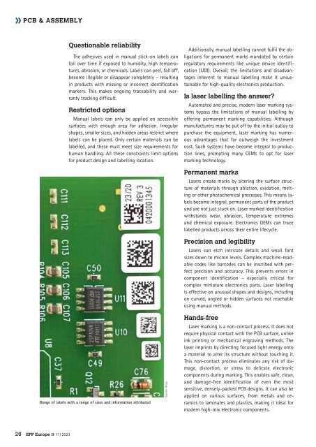
Range of labels with a range of sizes and information attributed<br />
Source: Altus<br />
Permanent marks<br />
Lasers create marks by altering the surface structure<br />
of materials through ablation, oxidation, melting<br />
or other photochemical processes. This means labels<br />
become integral, permanent parts of the product<br />
and are not just stuck on. Laser marked identification<br />
withstands wear, abrasion, temperature extremes<br />
and chemical exposure. Electronics OEMs can trace<br />
labelled products across their entire lifecycle.<br />
Precision and legibility<br />
Lasers can etch intricate details and small font<br />
sizes down to micron levels. Complex machine-readable<br />
codes like barcodes can be inscribed with perfect<br />
precision and accuracy. This prevents errors in<br />
component identification – especially critical for<br />
complex miniature electronics parts. Laser labelling<br />
is effective on unusual shapes and designs, including<br />
on curved, angled or hidden surfaces not reachable<br />
using manual methods.<br />
Hands-free<br />
Laser marking is a non-contact process. It does not<br />
require physical contact with the PCB surface, unlike<br />
ink printing or mechanical engraving methods. The<br />
laser imprints by directing focused light energy onto<br />
a material to alter its structure without touching it.<br />
This non-contact process eliminates any risk of damage,<br />
distortion, or stress to delicate electronic<br />
components during marking. This enables safe, clean,<br />
and damage-free identification of even the most<br />
sensitive, densely-packed PCB designs. It can also be<br />
applied on various surfaces, from metals and ceramics<br />
to laminates and plastics, making it ideal for<br />
modern high-mix electronic components.<br />
28 <strong>EPP</strong> <strong>Europe</strong> » 11 | 2023