channel - Advances in Electronics and Telecommunications
channel - Advances in Electronics and Telecommunications
channel - Advances in Electronics and Telecommunications

Create successful ePaper yourself
Turn your PDF publications into a flip-book with our unique Google optimized e-Paper software.
NOGUET et al.: CONSIDERING MICROELECTRONIC TRENDS IN ADVANCED WIRELESS SYSTEM DESIGN 113<br />
II. TRENDS IN SILICON TECHNOLOGIES<br />
Wireless technology has benefited from the advances the<br />
silicon technology has offered <strong>in</strong> the 1990s <strong>and</strong> 2000s. The<br />
whole telecommunication mutation from the analog doma<strong>in</strong><br />
to the digital realm has <strong>in</strong> fact been made possible by the<br />
m<strong>in</strong>iaturisation of transistors, lead<strong>in</strong>g to higher density though<br />
with low power efficient ICs. In turn, this move to digital<br />
communication has created the boom of the digital ICT at<br />
all layers, from broadb<strong>and</strong> communications to multimedia<br />
services. With this <strong>in</strong> m<strong>in</strong>d, it would not make sense to<br />
foresee what telecommunication will offer <strong>in</strong> the future without<br />
consider<strong>in</strong>g the trends <strong>in</strong> silicon technology research <strong>and</strong><br />
<strong>in</strong>dustry. The key factor beh<strong>in</strong>d the digital revolution has been<br />
the CMOS technology down-scal<strong>in</strong>g follow<strong>in</strong>g the so-called<br />
Moores Law which co<strong>in</strong>ed <strong>in</strong> the early 70s that the number<br />
of transistors would double every year. Although this rule has<br />
been validated over the 40 last years by the silicon <strong>in</strong>dustry<br />
<strong>and</strong> by the ITRS [2], it is agreed that we are com<strong>in</strong>g to a new<br />
era where this rule is no longer valid. Several reasons can be<br />
identified:<br />
• The physics of silicon <strong>in</strong>troduces side effects <strong>in</strong> deep submicron<br />
technology,<br />
• Predictability of transistors behaviour is gett<strong>in</strong>g less accurate,<br />
lead<strong>in</strong>g to lower yield or less optimal usage of<br />
silicon,<br />
• Power density is go<strong>in</strong>g to levels beyond what cool<strong>in</strong>g can<br />
offer,<br />
• Static power <strong>in</strong>creases which makes no longer valid the<br />
assumption that the overall power consumption decreases<br />
as transistors shr<strong>in</strong>k,<br />
• Investments needed for new deep sub-micron CMOS are<br />
be<strong>in</strong>g so huge that only less than a h<strong>and</strong>ful of application<br />
justifies it.<br />
For all these reasons, it is likely that we are on the verge of<br />
significant changes <strong>in</strong> the silicon capability roadmap, which<br />
make the analysis of future trends useful. Indeed, it is foreseen<br />
that the roadmap has to move from a pure down-scal<strong>in</strong>g to new<br />
functionalities <strong>and</strong> comb<strong>in</strong>ed technology vs. system <strong>in</strong>novation<br />
<strong>in</strong> order to manage future power, variability <strong>and</strong> complexity<br />
issues. However, there is no accepted c<strong>and</strong>idate today to<br />
replace CMOS devices consider<strong>in</strong>g the four essential metrics<br />
needed for successful applications: dimension (scalability),<br />
switch<strong>in</strong>g speed, energy consumption <strong>and</strong> throughput [4], [5].<br />
Moreover, when other metrics such as reliability, designability,<br />
<strong>and</strong> mixed-signal capability are added, the dom<strong>in</strong>ance<br />
of CMOS is even more obvious. It is then realistic to th<strong>in</strong>k<br />
that other micro or nano-technologies should be seen as future<br />
add-ons to CMOS <strong>and</strong> not as a substitute for it [6]. This<br />
transition between the “bus<strong>in</strong>ess as usual” era <strong>and</strong> the entry to<br />
the post 2015 1 period where new alternative or complementary<br />
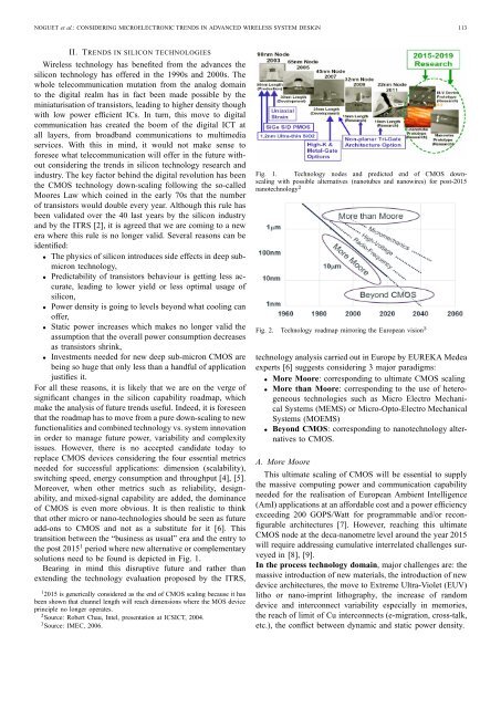
solutions need to be found is depicted <strong>in</strong> Fig. 1.<br />
Bear<strong>in</strong>g <strong>in</strong> m<strong>in</strong>d this disruptive future <strong>and</strong> rather than<br />
extend<strong>in</strong>g the technology evaluation proposed by the ITRS,<br />
1 2015 is generically considered as the end of CMOS scal<strong>in</strong>g because it has<br />
been shown that <strong>channel</strong> length will reach dimensions where the MOS device<br />
pr<strong>in</strong>ciple no longer operates.<br />
2 Source: Robert Chau, Intel, presentation at ICSICT, 2004.<br />
3 Source: IMEC, 2006.<br />
Fig. 1. Technology nodes <strong>and</strong> predicted end of CMOS downscal<strong>in</strong>g<br />
with possible alternatives (nanotubes <strong>and</strong> nanowires) for post-2015<br />
nanotechnology 2<br />
Fig. 2. Technology roadmap mirror<strong>in</strong>g the European vision 3<br />
technology analysis carried out <strong>in</strong> Europe by EUREKA Medea<br />
experts [6] suggests consider<strong>in</strong>g 3 major paradigms:<br />
• More Moore: correspond<strong>in</strong>g to ultimate CMOS scal<strong>in</strong>g<br />
• More than Moore: correspond<strong>in</strong>g to the use of heterogeneous<br />
technologies such as Micro Electro Mechanical<br />
Systems (MEMS) or Micro-Opto-Electro Mechanical<br />
Systems (MOEMS)<br />
• Beyond CMOS: correspond<strong>in</strong>g to nanotechnology alternatives<br />
to CMOS.<br />
A. More Moore<br />
This ultimate scal<strong>in</strong>g of CMOS will be essential to supply<br />
the massive comput<strong>in</strong>g power <strong>and</strong> communication capability<br />
needed for the realisation of European Ambient Intelligence<br />
(AmI) applications at an affordable cost <strong>and</strong> a power efficiency<br />
exceed<strong>in</strong>g 200 GOPS/Watt for programmable <strong>and</strong>/or reconfigurable<br />
architectures [7]. However, reach<strong>in</strong>g this ultimate<br />
CMOS node at the deca-nanometre level around the year 2015<br />
will require address<strong>in</strong>g cumulative <strong>in</strong>terrelated challenges surveyed<br />
<strong>in</strong> [8], [9].<br />
In the process technology doma<strong>in</strong>, major challenges are: the<br />
massive <strong>in</strong>troduction of new materials, the <strong>in</strong>troduction of new<br />
device architectures, the move to Extreme Ultra-Violet (EUV)<br />
litho or nano-impr<strong>in</strong>t lithography, the <strong>in</strong>crease of r<strong>and</strong>om<br />
device <strong>and</strong> <strong>in</strong>terconnect variability especially <strong>in</strong> memories,<br />
the reach of limit of Cu <strong>in</strong>terconnects (e-migration, cross-talk,<br />
etc.), the conflict between dynamic <strong>and</strong> static power density.