Teraflop 73 - Novembre - cesca
Teraflop 73 - Novembre - cesca
Teraflop 73 - Novembre - cesca

Create successful ePaper yourself
Turn your PDF publications into a flip-book with our unique Google optimized e-Paper software.
ones, are the focus of attention of scientists<br />
working in this field.<br />
Single-wall carbon nanotubes<br />
have many fascinating properties, the<br />
first of which is their structure. The<br />
length of a nanotube is typically much<br />
larger than its diameter, and thus nanotubes<br />
are essentially quasi-one dimensional<br />
systems. Furthermore, a<br />
graphene layer can be rolled-up to<br />
form a cylinder in a number of different<br />
ways, and the structure that results<br />
can be chiral or achiral (superposable<br />
onto its mirror image). Depending<br />
on its rolling pattern and diameter,<br />
a nanotube can be metallic or<br />
semiconducting, and yet we are always<br />
talking of the same material!<br />
This metallic/semiconducting behaviour<br />
was predicted theoretically in the<br />
early days of nanotubes, well before it<br />
was confirmed by experiments. The<br />
experiments which confirmed these<br />
theoretical predictions, performed using<br />
a scanning tunnelling microscope<br />
by the group of Cees Dekker at the<br />
university of Delft, in Holand, constitute<br />
one of the most impressive series<br />
of experiments probing the nanoscale<br />
yet reported in the literature. The<br />
scanning tunnelling microscope was<br />
used in two different ways. Firstly, with<br />
its nanoscale tip held above a previously<br />
located nanotube, the microscope<br />
was used to record the tunnelling<br />
current between the tip and<br />
the nanotube, as a function of the applied<br />
voltage. This provides a direct<br />
measurement of the electronic density<br />
of states of the nanotube, from<br />
where it can be deduced if the nanotube<br />
in question was a metallic or a<br />
semiconducting one. Secondly, the<br />
scanning tunnelling microscope was<br />
used to obtain an atomically resolved<br />
image of the nanotube for wich the<br />
electronic density of states had been<br />
previously observed. Within the uncertainty<br />
limits of the experiment, it<br />
was possible to fully confirm the theoretical<br />
predictions made on the correlation<br />
between electronic properties<br />
and structure in single-wall carbon<br />
nanotubes.<br />
The ever increasing trend of<br />
miniaturisation in electronics has already<br />
pushed the limits of technology<br />
down to the micrometer scale, and far<br />
from diminishing, this trend is steadily<br />
pushing further towards the nanometer<br />
scale. Because of their high aspect<br />
ratio (quotient of length over diameter),<br />
and their nanometer diameter,<br />
metallic nanotubes can be regarded<br />
as essentially one-dimensional conductors,<br />
and this makes them ideally<br />
suited as components of nanoscale<br />
electronic devices. Furthermore, it<br />
turns out that the electronic properties<br />
of nanotubes are sensitive to the<br />
chemical environment in which the<br />
nanotubes find themselves, and this<br />
has brought about the possibility of<br />
constructing chemical sensors based<br />
on nanotubes. Nanotubes can also be<br />
made to emit electrons from their tips<br />
when placed in an appropriately directed<br />
electric field, and this has lead<br />
to the fabrication of flat panel displays<br />
based on nanotubes.<br />
But the electronic properties of<br />
nanotubes are not the only ones that<br />
make them interesting. The carboncarbon<br />
bond in a graphene layer is<br />
probably the strongest chemical bond<br />
in an extended system in nature, and,<br />
since nanotubes are nothing but<br />
rolled-up graphene, this results in extraordinary<br />
mechanical properties; in<br />
fact, the Young´s modulus of carbon<br />
nanotubes is the highest that has ever<br />
been measured for any material, other<br />
than graphite itself. This brings<br />
about the possibility of using nanotubes<br />
to obtain highly resistant lightweight<br />
composite materials, which<br />
could be useful for coating many<br />
things, from spacecrafts to bulletproof<br />
jackets.<br />
This is but a short list of the potential<br />
applications of nanotubes,<br />
many of which have been demonstrated<br />
at the level of laboratory prototypes,<br />
and there are probably many<br />
more to come in the future. However,<br />
the main hurdle to be overcome before<br />
nanotubes and related structures<br />
can be effectively exploited in technological<br />
applications is the cost of<br />
their production. At present, the existing<br />
synthesis techniques are too expensive,<br />
have too little yield and<br />
specificity to be commercially viable.<br />
A great deal of research effort is devoted<br />
to obtain a better understanding<br />
of the growth mechanisms of nanotubes,<br />
so that better and more effective<br />
synthesis techniques can be<br />
found, which will clear the road to industrial<br />
applications of nanotubes. ■<br />
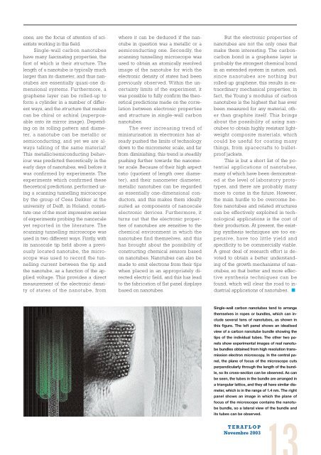
Single-wall carbon nanotubes tend to arrange<br />
themselves in ropes or bundles, which can include<br />
several tens of nanotubes, as shown in<br />
this figure. The left panel shows an idealised<br />
view of a carbon nanotube bundle showing the<br />
tips of the individual tubes. The other two panels<br />
show experimental images of real nanotube<br />
bundles obtained from high resolution transmission<br />
electron microscopy. In the central panel,<br />
the plane of focus of the microscope cuts<br />
perpendicularly through the length of the bundle,<br />
so its cross-section can be observed. As can<br />
be seen, the tubes in the bundle are arranged in<br />
a triangular lattice, and they all have similar diameter,<br />
which is in the range of 1.4 nm. The right<br />
panel shows an image in which the plane of<br />
focus of the microscope contains the nanotube<br />
bundle, so a lateral view of the bundle and<br />
its tubes can be observed.<br />
TERAFLOP<br />
<strong>Novembre</strong> 2003