Teraflop 73 - Novembre - cesca
Teraflop 73 - Novembre - cesca
Teraflop 73 - Novembre - cesca

Create successful ePaper yourself
Turn your PDF publications into a flip-book with our unique Google optimized e-Paper software.
One of the great challenges of<br />
modern science is how to fabricate<br />
and manipulate materials<br />
and devices at the molecular scale.<br />
For example, nowadays most commercial<br />
semiconductor technologies (such<br />
as standard MOS technology) use bulk<br />
material properties in order to produce<br />
electronic circuits. Also current lithographic<br />
methods used in production of<br />
microchips may only operate with structures<br />
of ~200 nm of more in size. Going<br />
below this limit requires new experimental,<br />
not currently in production, techniques.<br />
Indeed, recently, there has been<br />
an explosion of research on the<br />
nanoscale behavior (nanoscale is defined<br />
as objects of 1-100 nm in length).<br />
Nanoscience and nanotechnology involve<br />
studying and working with matter<br />
on an ultra-small scale (a single human<br />
hair is around 80,000 nm in width).<br />
Nanoscience is an interdisciplinary field<br />
of sciences which in the next 10-20<br />
years is expected to have great impact<br />
on technology and stretches across the<br />
whole spectrum of science, influencing<br />
medicine, biology, physics, engineering,<br />
chemistry etc. Nanotechnology<br />
which is mostly studied now includes<br />
molecular electronics, nanocrystalline<br />
materials, NEMS, nanoparticles, quantum<br />
dots and nanotubes. From these<br />
applications we will discuss only nanotubes<br />
and their smaller counterparts,<br />
fullerenes.<br />
An unique character of nanoscience<br />
is that it creates devices through<br />
“bottom-up” instead of “top-down” approach<br />
and major problem of nanoscience<br />
is how we can study (observe)<br />
the nanoobjects. Another reason for the<br />
explosion in nanoscience, starting from<br />
the late 90’s is the developments in the<br />
80’s of different microscopy types, such<br />
as STM, AFM, SEM and TEM. They<br />
Single Wall Carbon Nanotube<br />
Solubility and Novel C60 Materials<br />
Michael Bendikov and Fred Wudl<br />
Department of Chemistry and Biochemistry<br />
Exotic Materials Institute<br />
University of California, Los Angeles, California<br />
provide the “eyes” and “fingers” for<br />
nanoscale manipulation and measurements.<br />
Recent progress in high performance<br />
computers also allowed highly<br />
sophisticated computer simulations<br />
which are essential to enhance our<br />
understanding of the processes occurring<br />
on the nanoscale regime, as well<br />
as to design “tailor-made” materials.<br />
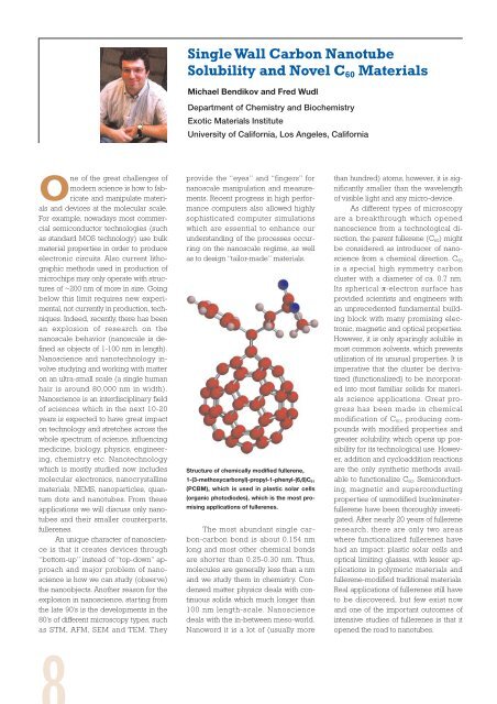
Structure of chemically modified fullerene,<br />
1-(3-methoxycarbonyl)-propyl-1-phenyl-(6,6)C 61<br />
(PCBM), which is used in plastic solar cells<br />
(organic photodiodes), which is the most promising<br />
applications of fullerenes.<br />
The most abundant single carbon-carbon<br />
bond is about 0.154 nm<br />
long and most other chemical bonds<br />
are shorter than 0.25-0.30 nm. Thus,<br />
molecules are generally less than a nm<br />
and we study them in chemistry. Condensed<br />
matter physics deals with continuous<br />
solids which much longer than<br />
100 nm length-scale. Nanoscience<br />
deals with the in-between meso-world.<br />
Nanoword it is a lot of (usually more<br />
than hundred) atoms, however, it is significantly<br />
smaller than the wavelength<br />
of visible light and any micro-device.<br />
As different types of microscopy<br />
are a breakthrough which opened<br />
nanoscience from a technological direction,<br />
the parent fullerene (C 60) might<br />
be considered as introducer of nanoscience<br />
from a chemical direction. C 60<br />
is a special high symmetry carbon<br />
cluster with a diameter of ca. 0.7 nm.<br />
Its spherical π-electron surface has<br />
provided scientists and engineers with<br />
an unprecedented fundamental building<br />
block with many promising electronic,<br />
magnetic and optical properties.<br />
However, it is only sparingly soluble in<br />
most common solvents, which prevents<br />
utilization of its unusual properties. It is<br />
imperative that the cluster be derivatized<br />
(functionalized) to be incorporated<br />
into most familiar solids for materials<br />
science applications. Great progress<br />
has been made in chemical<br />
modification of C 60, producing compounds<br />
with modified properties and<br />
greater solubility, which opens up possibility<br />
for its technological use. However,<br />
addition and cycloaddition reactions<br />
are the only synthetic methods available<br />
to functionalize C 60. Semiconducting,<br />
magnetic and superconducting<br />
properties of unmodified buckminsterfullerene<br />
have been thoroughly investigated.<br />
After nearly 20 years of fullerene<br />
research, there are only two areas<br />
where functionalized fullerenes have<br />
had an impact: plastic solar cells and<br />
optical limiting glasses, with lesser applications<br />
in polymeric materials and<br />
fullerene-modified traditional materials.<br />
Real applications of fullerenes still have<br />
to be discovered, but few exist now<br />
and one of the important outcomes of<br />
intensive studies of fullerenes is that it<br />
opened the road to nanotubes.