Teraflop 73 - Novembre - cesca
Teraflop 73 - Novembre - cesca
Teraflop 73 - Novembre - cesca

You also want an ePaper? Increase the reach of your titles
YUMPU automatically turns print PDFs into web optimized ePapers that Google loves.
Carbon nanotubes are one of the<br />
most commonly mentioned building<br />
blocks of nanotechnology. One of the<br />
major classifications of carbon nanotubes<br />
is into single-walled (SWNTs),<br />
which have a single cylindrical wall,<br />
and multi-walled (MWNTs), which<br />
have cylinders within cylinders. SWNT<br />
can be represented as an infinite tube<br />
of carbon hexagons (or two dimensional<br />
graphene sheet rolled into a<br />
tube) with open ends or caped by<br />
half-fullerene-like ends. They are<br />
grown now by several techniques in<br />
the laboratory and are from 0.7 nm up<br />
to few nanometers in diameter and<br />
several microns long. The detailed<br />
mechanisms responsible for nanotube<br />
growth are still not fully understood and<br />
computer modeling is playing an increasing<br />
role in understanding of this<br />
important process. The aspect ratio is<br />
very high and can be up to 10,000. The<br />
beauty of the nanotubes is that they<br />
possess all properties of nanoobjects,<br />
yet they can be treated as molecules.<br />
SWNT can be metallic or semiconducting<br />
just depending on how a<br />
graphene sheet was rolled and this offer<br />
amazing possibilities to create future nanoelectronics<br />
devices and circuits. Due<br />
to the tubular structure and since all carbon<br />
atoms are three coordinated in the<br />
nanotube, all chemical bonds in carbon<br />
nanotubes are stronger than in other organic<br />
compounds. As a result, nanotubes<br />
exhibit extraordinary mechanical<br />
properties: the Young's modulus is<br />
over 1 Tera Pascal. It is comparable to<br />
diamond. The estimated tensile strength<br />
is 200 Giga Pascal (about one hundred<br />
times stronger than steel) and electrical<br />
conductivity clamed to be similar to<br />
copper. These properties are ideal for<br />
reinforced composites and nanoelectromechanical<br />
systems (NEMS).<br />
However, despite the extraordinary<br />
promise of carbon nanotubes, their realistic<br />
application in materials and<br />
devices has been hindered by processing<br />
and manipulation difficulties.<br />
As in the case of fullerenes,<br />
chemical modification of nanotubes<br />
should be important to design of new<br />
materials. However, again, solubility is<br />
probably the main issue. The principal<br />
initial challenge was to make the carbon<br />
nanotubes soluble in water and<br />
the solvents of traditional organic<br />
chemistry. In order to do this it was<br />
necessary to defeat the huge van der<br />
Waals binding energy that nanotubes<br />
have when they align side to side, estimated<br />
to be roughly 12 kcal/mol for<br />
Structure of (up) (14,0) “zigzag” nanotube which has semiconductor bandgap and (down) (6,6)<br />
“armchair” nanotube, which has metallic bandgap.<br />
each nm of contact length. This is such<br />
a large cohesive energy that the tubes<br />
are invariably found to be assembled<br />
in close packed "ropes," hundreds of<br />
tubes in cross-section, and many<br />
microns in length. Much progress was<br />
made in nanotube solubilization in recent<br />
years and today methods exist<br />
which allow to process nanotubes<br />
from solution. One way of making a<br />
nanotube interact with something else<br />
is to modify it chemically. This is being<br />
explored not just for composite applications<br />
but also for a variety of other<br />
applications, such as biosensors. Another<br />
application of nanotubes which<br />
was developed in our group is a nanotube<br />
polarizer. This device transmits<br />
polarized light anisotropically using<br />
aligned nanotubes and taking advantage<br />
of their high aspect ratio.<br />
The main long-term applications<br />
of nanotubes will probably be as advanced<br />
materials; however, wider applications<br />
are also expected. Nanotubes<br />
are already being shipped on<br />
the tip of atomic force microscope<br />
probes to enhance atomic-resolution<br />
imaging. Nanotube-based chemical<br />
and bio-sensors should be on the market<br />
soon. The thermal conductivity of<br />
nanotubes shows promise in applications<br />
from cooling integrated circuits to<br />
aerospace materials. The versatility of<br />
nanotubes does suggest that they<br />
might one day rank as one of the most<br />
important materials ever discovered;<br />
however, challenges are still high.<br />
In conclusions, up to now we<br />
have seen quite a lot of nanoscience,<br />
but little nanotechnology and in next<br />
years we will see how nanotechnology<br />
participates in our everyday life,<br />
similar to semiconductor technology<br />
50 years ago. ■<br />
TERAFLOP<br />
<strong>Novembre</strong> 2003<br />
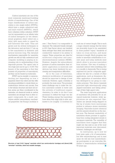
Example of graphene sheet.