Backside Circuit Edit on Device Level - New Methodologies - Imec
Backside Circuit Edit on Device Level - New Methodologies - Imec
Backside Circuit Edit on Device Level - New Methodologies - Imec

You also want an ePaper? Increase the reach of your titles
YUMPU automatically turns print PDFs into web optimized ePapers that Google loves.
1<br />
2<br />
3<br />
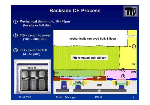
Mechanical thinning to 10 - 40µm<br />
(locally or full die)<br />
FIB - trench to n-well<br />
(100 - 600 µm 2 )<br />
FIB - trench to STI<br />
(4 - 50 µm 2 )<br />
bulk Si<br />
n-well<br />
c<strong>on</strong>trast<br />
7 µm STI<br />
150µm<br />
<str<strong>on</strong>g>Backside</str<strong>on</strong>g> CE Process<br />
NW<br />
W<br />
mechanically removed bulk Silic<strong>on</strong><br />
FIB removed bulk Silic<strong>on</strong><br />
Poly<br />
bulk-Si<br />
02.10.2006 Rudolf Schlangen EFUG 3<br />
STI<br />
IMD<br />
M1<br />
2<br />
3<br />
berlin<br />
1<br />
Si<br />
PW