Backside Circuit Edit on Device Level - New Methodologies - Imec
Backside Circuit Edit on Device Level - New Methodologies - Imec
Backside Circuit Edit on Device Level - New Methodologies - Imec

Create successful ePaper yourself
Turn your PDF publications into a flip-book with our unique Google optimized e-Paper software.
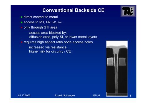
● direct c<strong>on</strong>tact to metal<br />
● access to M1, M2, M3, M4<br />
C<strong>on</strong>venti<strong>on</strong>al <str<strong>on</strong>g>Backside</str<strong>on</strong>g> CE<br />
● <strong>on</strong>ly through STI area<br />
access area blocked by:<br />
diffusi<strong>on</strong> area, poly-Si, or lower metal layers<br />
● requires high aspect ratio node access holes<br />
increased via resistance<br />
higher risk for circuitry / CE<br />
02.10.2006 Rudolf Schlangen EFUG 8<br />
berlin