Image sensor datasheet (PDF)
Image sensor datasheet (PDF)
Image sensor datasheet (PDF)

You also want an ePaper? Increase the reach of your titles
YUMPU automatically turns print PDFs into web optimized ePapers that Google loves.
OPERATION<br />
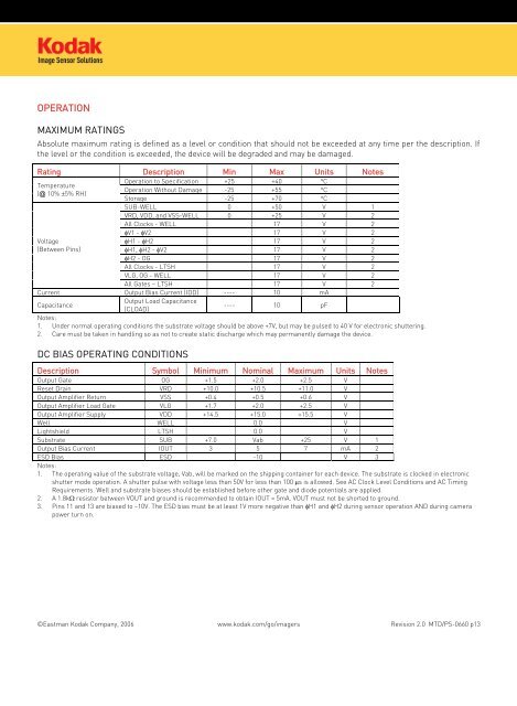
MAXIMUM RATINGS<br />
Absolute maximum rating is defined as a level or condition that should not be exceeded at any time per the description. If<br />
the level or the condition is exceeded, the device will be degraded and may be damaged.<br />
Rating Description Min Max Units Notes<br />
Operation to Specification +25 +40 °C<br />
Temperature<br />
Operation Without Damage -25 +55 °C<br />
(@ 10% ±5% RH)<br />
Storage -25 +70 °C<br />
SUB-WELL 0 +50 V 1<br />
VRD, VDD, and VSS-WELL 0 +25 V 2<br />
All Clocks - WELL 17 V 2<br />
φV1 - φV2 17 V 2<br />
Voltage<br />
φH1 - φH2 17 V 2<br />
(Between Pins)<br />
φH1, φH2 - φV2 17 V 2<br />
φH2 - OG 17 V 2<br />
All Clocks - LTSH 17 V 2<br />
VLG, OG - WELL 17 V 2<br />
All Gates – LTSH 17 V 2<br />
Current Output Bias Current (IDD) ---- 10 mA<br />
Capacitance<br />
Output Load Capacitance<br />
(CLOAD)<br />
---- 10 pF<br />
Notes:<br />
1. Under normal operating conditions the substrate voltage should be above +7V, but may be pulsed to 40 V for electronic shuttering.<br />
2. Care must be taken in handling so as not to create static discharge which may permanently damage the device.<br />
DC BIAS OPERATING CONDITIONS<br />
Description Symbol Minimum Nominal Maximum Units Notes<br />
Output Gate OG +1.5 +2.0 +2.5 V<br />
Reset Drain VRD +10.0 +10.5 +11.0 V<br />
Output Amplifier Return VSS +0.4 +0.5 +0.6 V<br />
Output Amplifier Load Gate VLG +1.7 +2.0 +2.5 V<br />
Output Amplifier Supply VDD +14.5 +15.0 +15.5 V<br />
Well WELL 0.0 V<br />
Lightshield LTSH 0.0 V<br />
Substrate SUB +7.0 Vab +25 V 1<br />
Output Bias Current IOUT 3 5 7 mA 2<br />
ESD Bias ESD -10 V 3<br />
Notes:<br />
1. The operating value of the substrate voltage, Vab, will be marked on the shipping container for each device. The substrate is clocked in electronic<br />
shutter mode operation. A shutter pulse with voltage less than 50V for less than 100 µs is allowed. See AC Clock Level Conditions and AC Timing<br />
Requirements. Well and substrate biases should be established before other gate and diode potentials are applied.<br />
2. A 1.8kΩ resistor between VOUT and ground is recommended to obtain IOUT = 5mA. VOUT must not be shorted to ground.<br />
3. Pins 11 and 13 are biased to –10V. The ESD bias must be at least 1V more negative than φH1 and φH2 during <strong>sensor</strong> operation AND during camera<br />
power turn on.<br />
©Eastman Kodak Company, 2006 www.kodak.com/go/imagers Revision 2.0 MTD/PS-0660 p13