Image sensor datasheet (PDF)
Image sensor datasheet (PDF)
Image sensor datasheet (PDF)

You also want an ePaper? Increase the reach of your titles
YUMPU automatically turns print PDFs into web optimized ePapers that Google loves.
IMAGE ACQUISITION<br />
An electronic representation of an image is formed when<br />
incident photons falling on the <strong>sensor</strong> plane create<br />
electron-hole pairs within the individual silicon<br />
photodiodes. These photoelectrons are collected locally<br />
by the formation of potential wells at each photosite.<br />
Below photodiode saturation, the number of<br />
photoelectrons collected at each pixel is linearly<br />
dependent on light level and exposure time and nonlinearly<br />
dependent on wavelength. When the<br />
photodiode's charge capacity is reached, excess<br />
electrons are discharged into the substrate to prevent<br />
blooming.<br />
CHARGE TRANSPORT<br />
The accumulated or integrated charge from each<br />
photodiode is transported to the output by a three step<br />
process. The charge is first transported from the<br />
photodiodes to the VCCDs by applying a large positive<br />
voltage to the phase-one vertical clock (φV2). This reads<br />
out every row, or line, of photodiodes into the VCCDs.<br />
The charge is then transported from the VCCDs to the<br />
HCCDs line by line. Finally, the HCCDs transport these<br />
rows of charge packets to the output structures pixel by<br />
pixel. On each falling edge of the horizontal clock, φH2,<br />
these charge packets are dumped over the output gate<br />
(OG, Figure 2) onto the floating diffusion (FD Figure 2).<br />
Both the horizontal and vertical shift registers use<br />
traditional two-phase complementary clocking for<br />
charge transport. Transfer to the horizontal CDD begins<br />
when φV2 is brought low (and φV1 high) causing a line of<br />
charge to transfer from φV2 to φV1 and subsequently into<br />
the horizontal register. The sequence completes when<br />
φV1 is brought low before the horizontal CCD reads the<br />
first line of charge<br />
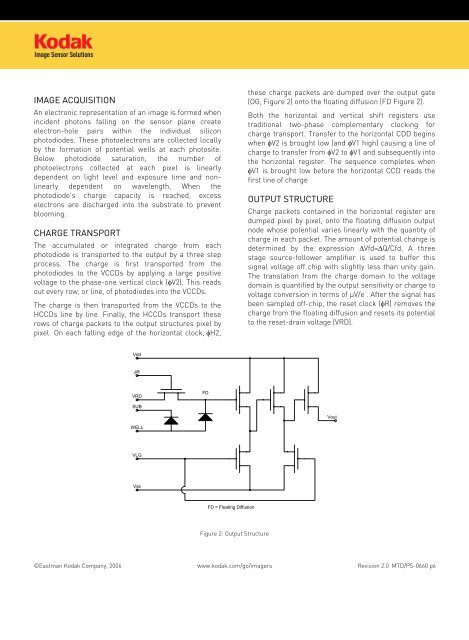
OUTPUT STRUCTURE<br />
Charge packets contained in the horizontal register are<br />
dumped pixel by pixel, onto the floating diffusion output<br />
node whose potential varies linearly with the quantity of<br />
charge in each packet. The amount of potential change is<br />
determined by the expression ∆Vfd=∆Q/Cfd. A three<br />
stage source-follower amplifier is used to buffer this<br />
signal voltage off chip with slightly less than unity gain.<br />
The translation from the charge domain to the voltage<br />
domain is quantified by the output sensitivity or charge to<br />
voltage conversion in terms of µV/e - . After the signal has<br />
been sampled off-chip, the reset clock (φR) removes the<br />
charge from the floating diffusion and resets its potential<br />
to the reset-drain voltage (VRD).<br />
Vdd<br />
φR<br />
VRD<br />
FD<br />
SUB<br />
Vout<br />
WELL<br />
VLG<br />
Vss<br />
FD = Floating Diffusion<br />
Figure 2: Output Structure<br />
©Eastman Kodak Company, 2006 www.kodak.com/go/imagers Revision 2.0 MTD/PS-0660 p6