
Create successful ePaper yourself
Turn your PDF publications into a flip-book with our unique Google optimized e-Paper software.
ADVANCE INFORMATION<br />
<strong>UAC</strong> <strong>357xB</strong><br />
5.6. Electrical Characteristics<br />
Abbreviations:<br />
tbd = to be defined<br />
vacant = not applicable<br />
positive current values mean current flowing into the chip<br />
5.6.1. Absolute Maximum Ratings<br />
Stresses beyond those listed in the “Absolute Maximum Ratings” may cause permanent damage to the device. This<br />
is a stress rating only. Functional operation of the device at these conditions is not implied. Exposure to absolute<br />
maximum rating conditions for extended periods will affect device reliability.<br />
This device contains circuitry to protect the inputs and outputs against damage due to high static voltages or electric<br />
fields; however, it is advised that normal precautions be taken to avoid application of any voltage higher than absolute<br />
maximum-rated voltages to this high-impedance circuit.<br />
All voltages listed are referenced to ground except where noted.<br />
All GND pins must be connected to a low-resistive ground plane close to the IC.<br />
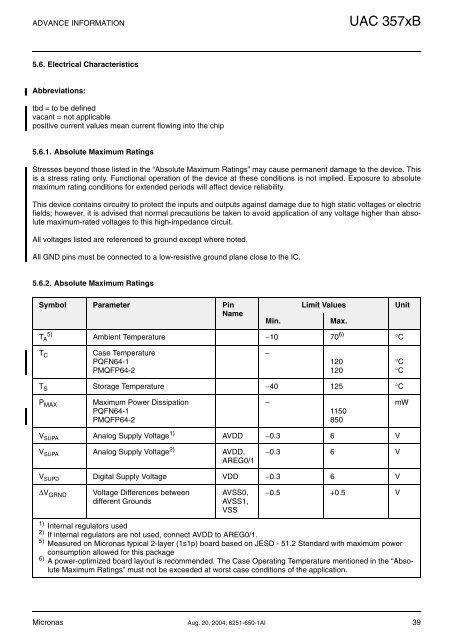
5.6.2. Absolute Maximum Ratings<br />
Symbol Parameter Pin<br />
Name<br />
Min.<br />
Limit Values<br />
Max.<br />
Unit<br />
T A<br />
5)<br />
Ambient Temperature −10 70 6) °C<br />
T C<br />
Case Temperature<br />
PQFN64-1<br />
PMQFP64-2<br />
–<br />
120<br />
120<br />
°C<br />
°C<br />
T S Storage Temperature −40 125 °C<br />
P MAX<br />
Maximum Power Dissipation<br />
PQFN64-1<br />
PMQFP64-2<br />
–<br />
1150<br />
850<br />
mW<br />
V SUPA Analog Supply Voltage 1) AVDD −0.3 6 V<br />
V SUPA Analog Supply Voltage 2) AVDD,<br />
AREG0/1<br />
−0.3 6 V<br />
V SUPD Digital Supply Voltage VDD −0.3 6 V<br />
∆V GRND<br />
Voltage Differences between<br />
different Grounds<br />
AVSS0,<br />
AVSS1,<br />
VSS<br />
−0.5 +0.5 V<br />
1) Internal regulators used<br />
2) If internal regulators are not used, connect AVDD to AREG0/1.<br />
5) Measured on Micronas typical 2-layer (1s1p) board based on JESD - 51.2 Standard with maximum power<br />
consumption allowed for this package<br />
6) A power-optimized board layout is re<strong>com</strong>mended. The Case Operating Temperature mentioned in the “Absolute<br />
Maximum Ratings” must not be exceeded at worst case conditions of the application.<br />
Micronas Aug. 20, 2004; 6251-650-1AI 39