
You also want an ePaper? Increase the reach of your titles
YUMPU automatically turns print PDFs into web optimized ePapers that Google loves.
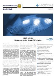
ADVANCE INFORMATION<br />
<strong>UAC</strong> <strong>357xB</strong><br />
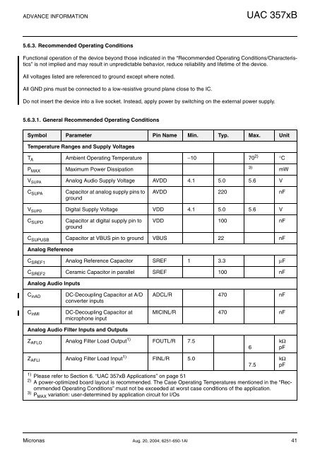
5.6.3. Re<strong>com</strong>mended Operating Conditions<br />
Functional operation of the device beyond those indicated in the “Re<strong>com</strong>mended Operating Conditions/Characteristics”<br />
is not implied and may result in unpredictable behavior, reduce reliability and lifetime of the device.<br />
All voltages listed are referenced to ground except where noted.<br />
All GND pins must be connected to a low-resistive ground plane close to the IC.<br />
Do not insert the device into a live socket. Instead, apply power by switching on the external power supply.<br />
5.6.3.1. General Re<strong>com</strong>mended Operating Conditions<br />
Symbol Parameter Pin Name Min. Typ. Max. Unit<br />
Temperature Ranges and Supply Voltages<br />
T A Ambient Operating Temperature −10 70 2) °C<br />
P MAX<br />
Maximum Power Dissipation<br />
3)<br />
mW<br />
V SUPA Analog Audio Supply Voltage AVDD 4.1 5.0 5.6 V<br />
C SUPA<br />
Capacitor at analog supply pins to<br />
ground<br />
AVDD 220 nF<br />
V SUPD Digital Supply Voltage VDD 4.1 5.0 5.6 V<br />
C SUPD<br />
Capacitor at digital supply pin to<br />
ground<br />
VDD 100 nF<br />
C SUPUSB Capacitor at VBUS pin to ground VBUS 22 nF<br />
Analog Reference<br />
C SREF1 Analog Reference Capacitor SREF 1 3.3 µF<br />
C SREF2 Ceramic Capacitor in parallel SREF 100 nF<br />
Analog Audio Inputs<br />
C inAD<br />
C inMI<br />
DC-Decoupling Capacitor at A/D<br />
converter inputs<br />
DC-Decoupling Capacitor at<br />
microphone input<br />
ADCL/R 470 nF<br />
MICINL/R 470 nF<br />
Analog Audio Filter Inputs and Outputs<br />
Z AFLO Analog Filter Load Output 1) FOUTL/R 7.5<br />
Z AFLI Analog Filter Load Input 1) FINL/R 5.0<br />
6<br />
7.5<br />
kΩ<br />
pF<br />
kΩ<br />
pF<br />
1) Please refer to Section 6. “<strong>UAC</strong> <strong>357xB</strong> Applications” on page 51<br />
2) A power-optimized board layout is re<strong>com</strong>mended. The Case Operating Temperatures mentioned in the “Re<strong>com</strong>mended<br />
Operating Conditions” must not be exceeded at worst case conditions of the application.<br />
3) P MAX variation: user-determined by application circuit for I/Os<br />
Micronas Aug. 20, 2004; 6251-650-1AI 41