Nuts & Volts
Nuts & Volts
Nuts & Volts

Create successful ePaper yourself
Turn your PDF publications into a flip-book with our unique Google optimized e-Paper software.
CODING AND<br />
ACTIVATING THE<br />
MC68HC908MR16 ADC<br />
Looking at the MC68HC908MR16<br />
datasheet, I found that the MC68HC<br />
908MR16 houses a 10-channel analogto-digital<br />
converter module with<br />
10 bits of resolution (0x3FF or<br />
0b1111111111 full scale). In a nutshell,<br />
the MC68HC908MR16 employs an<br />
analog multiplexer to select one of 10<br />
analog input channels that feed<br />
a successive approximation-based<br />
analog-to-digital converter subsystem,<br />
which signals the end of an analog-todigital<br />
conversion by raising a flag or<br />
generating an interrupt request. The 10-<br />
bit analog-to-digital conversion result<br />
is placed in a pair of special-purpose<br />
MC68HC908MR16 data registers, ADRH<br />
and ARDL. For now, let’s put the<br />
MC68HC908MR16 datasheet aside and<br />
see what the ADC Bean can do for us.<br />
The BEAN configuration process<br />
for the ADC BEAN is identical to that<br />
of the RS-232 and LED_BIT Beans we<br />
configured previously. I accessed the<br />
Bean Selector window and doubleclicked<br />
the ADC Bean to insert it into<br />
the new ADC project, which is called<br />
MR16_ADC. I noticed that the analog<br />
input was assigned to the I/O pin that<br />
I was using for the LED. I still want to<br />
blink the LED as a run indicator and I<br />
don’t want to change or throw away<br />
the LED code I’ve already written. So,<br />
I deleted the newly inserted ADC<br />
Bean and moved to the Port I/O<br />
folder in the Bean Selector window.<br />
Once there, I double-clicked on the<br />
BitIO Bean and inserted it into my new<br />
MR16_ADC project. Once I saw that the<br />
LED had once again assumed my<br />
desired position on Port B, I configured<br />
the LED_BIT Bean to match the<br />
configuration I laid out in the previous<br />
RS-232 application we just discussed. I<br />
then reinserted the ADC Bean, saw that<br />
it was assigned to the next available<br />
Port B I/O pin, named it ANALOG, and<br />
started the Bean configuration process.<br />
The Bean Inspector wouldn’t let<br />
me enter anything that would<br />
jeopardize the functionality of the<br />
MC68HC908MR16 analog-to-digital<br />
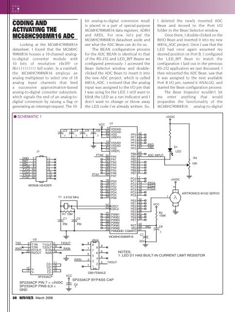
■ SCHEMATIC 1<br />
+5VDC<br />
TXD<br />
RXD<br />
GND 2<br />
RST 4<br />
IRQ 6<br />
PTA0 8<br />
PTC2 10<br />
PTC3 12<br />
PTC4 14<br />
PTA7 16<br />
2<br />
1<br />
3<br />
20<br />
12<br />
17<br />
U3<br />
T1IN<br />
T2IN<br />
R1OUT<br />
R2OUT<br />
V-<br />
V-<br />
J1<br />
1<br />
3<br />
5<br />
7<br />
9<br />
11<br />
13<br />
15<br />
MON08 HEADER<br />
T1OUT<br />
T2OUT<br />
R1IN<br />
R2IN<br />
C2+<br />
C2+<br />
C2-<br />
C2-<br />
SP233ACP<br />
28 March 2006<br />
5<br />
18<br />
4<br />
19<br />
11<br />
15<br />
16<br />
10<br />
SP233ACP PIN 7 = +5VDC<br />
SP233ACP PINS 6,9 =<br />
GND<br />
C3<br />
.1<br />
C1<br />
20p<br />
TXOUT<br />
RXIN<br />
C4<br />
.1<br />
Y1 4.9152 MHz<br />
R1 10M<br />
DB9 FEMALE<br />
VCC<br />
SP233ACP BYPASS CAP<br />
C9<br />
.1<br />
C2<br />
20p<br />
RXIN<br />
C5<br />
.1<br />
9<br />
7<br />
5<br />
3<br />
1<br />
PTA7<br />
JR2A<br />
9<br />
VCC U1<br />
9<br />
VDDAD<br />
C6 50<br />
40<br />
VDDAD<br />
.1 12<br />
VDD<br />
VREFH<br />
10<br />
54<br />
VSSAD<br />
41<br />
VSSAD<br />
11<br />
VSS<br />
VREFL<br />
7 8<br />
5 6<br />
3 4<br />
1 2<br />
PTA0<br />
8<br />
6<br />
4<br />
2<br />
55<br />
56<br />
57<br />
58<br />
59<br />
60<br />
61<br />
62<br />
18<br />
19<br />
20<br />
21<br />
22<br />
23<br />
24<br />
52<br />
53<br />
25<br />
26<br />
27<br />
28<br />
30<br />
PA0<br />
PA1<br />
PA2<br />
PA3<br />
PA4<br />
PA5<br />
PA6<br />
PA7<br />
PD0<br />
PD1<br />
PD2<br />
PD3<br />
PD4<br />
PD5<br />
PD6<br />
OSC1<br />
OSC2<br />
PWM1<br />
PWM2<br />
PWM3<br />
PWM4<br />
PWM5<br />
31<br />
29<br />
PWM6<br />
PWMGND<br />
MC68HC908MR16<br />
TXOUT<br />
PF0<br />
42<br />
PF1<br />
43<br />
PF2<br />
44<br />
PF3<br />
45<br />
PF4<br />
46<br />
PF5<br />
47<br />
PB0<br />
PB1<br />
PB2<br />
PB3<br />
PB4<br />
PB5<br />
PB6<br />
PB7<br />
63<br />
64<br />
1<br />
2<br />
3<br />
4<br />
5<br />
6<br />
PC0<br />
7<br />
PC1<br />
8<br />
PC2<br />
13<br />
PC3<br />
14<br />
PC4<br />
15<br />
PC5<br />
16<br />
PC6<br />
17<br />
PE0<br />
32<br />
PE1<br />
33<br />
PE2<br />
34<br />
PE3<br />
35<br />
PE4<br />
36<br />
PE5<br />
37<br />
PE6<br />
38<br />
PE7<br />
39<br />
RST<br />
49<br />
IRQ<br />
48<br />
51<br />
CGMXFC<br />
C7<br />
.022<br />
RXD<br />
TXD<br />
ADC INPUT<br />
PTC2<br />
PTC3<br />
PTC4<br />
IRQ<br />
VCC<br />
R2<br />
100K<br />
C8<br />
.1<br />
1<br />
D1<br />
LED<br />
+5VDC<br />
3<br />
+<br />
A<br />
-<br />
2<br />
R3<br />
10K<br />
AIRTRONICS 94102 SERVO<br />
NOTES:<br />
1. LED D1 HAS BUILT-IN CURRENT LIMIT RESISTOR